


Part No. E2047Q70300R
REV-Q703
Mini-ITX Qseven Carrier Board
User’s Manual
1st Ed – 20 October 2015

REV-Q703
2 REV-Q703 User’s Manual
FCC Statement
THIS DEVICE COMPLIES WITH PART 15 FCC RULES. OPERATION IS
SUBJECT TO THE FOLLOWING TWO CONDITIONS:
(1) THIS DEVICE MAY NOT CAUSE HARMFUL INTERFERENCE.
(2) THIS DEVICE MUST ACCEPT ANY INTERFERENCE RECEIVED INCLUDING
INTERFERENCE THAT MAY CAUSE UNDESIRED OPERATION.
THIS EQUIPMENT HAS BEEN TESTED AND FOUND TO COMPLY WITH THE LIMITS
FOR A CLASS "A" DIGITAL DEVICE, PURSUANT TO PART 15 OF THE FCC RULES.
THESE LIMITS ARE DESIGNED TO PROVIDE REASONABLE PROTECTION AGAINST
HARMFUL INTERFERENCE WHEN THE EQUIPMENT IS OPERATED IN A
COMMERCIAL ENVIRONMENT. THIS EQUIPMENT GENERATES, USES, AND CAN
RADIATE RADIO FREQUENCY ENERGY AND, IF NOT INSTALLED AND USED IN
ACCORDANCE WITH THE INSTRUCTION MANUAL, MAY CAUSE HARMFUL
INTERFERENCE TO RADIO COMMUNICATIONS.
OPERATION OF THIS EQUIPMENT IN A RESIDENTIAL AREA IS LIKELY TO CAUSE
HARMFUL INTERFERENCE IN WHICH CASE THE USER WILL BE REQUIRED TO
CORRECT THE INTERFERENCE AT HIS OWN EXPENSE.
Notice
This guide is designed for experienced users to setup the system within the shortest time.
For detailed information, please always refer to the electronic user's manual.
Copyright Notice
Copyright 2015 Avalue Technology Inc., ALL RIGHTS RESERVED.
No part of this document may be reproduced, copied, translated, or transmitted in any form
or by any means, electronic or mechanical, for any purpose, without the prior written
permission of the original manufacturer.
Trademark Acknowledgement
Brand and product names are trademarks or registered trademarks of their respective
owners.
Disclaimer
Avalue Technology Inc. reserves the right to make changes, without notice, to any product,
including circuits and/or software described or contained in this manual in order to improve
design and/or performance. Avalue Technology assumes no responsibility or liability for the
use of the described product(s), conveys no license or title under any patent, copyright, or
masks work rights to these products, and makes no representations or warranties that

User’s Manual
REV-Q703 User’s Manual 3
these products are free from patent, copyright, or mask work right infringement, unless
otherwise specified. Applications that are described in this manual are for illustration
purposes only. Avalue Technology Inc. makes no representation or warranty that such
application will be suitable for the specified use without further testing or modification.
Life Support Policy
Avalue Technology’s PRODUCTS ARE NOT FOR USE AS CRITICAL COMPONENTS IN
LIFE SUPPORT DEVICES OR SYSTEMS WITHOUT THE PRIOR WRITTEN APPROVAL
OF Avalue Technology Inc.
As used herein:
1. Life support devices or systems are devices or systems which, (a) are intended for
surgical implant into body, or (b) support or sustain life and whose failure to perform,
when properly used in accordance with instructions for use provided in the labeling, can
be reasonably expected to result in significant injury to the user.
2. A critical component is any component of a life support device or system whose
failure to perform can be reasonably expected to cause the failure of the life
support device or system, or to affect its safety or effectiveness.
A Message to the Customer
Avalue Customer Services
Each and every Avalue’s product is built to the most exacting specifications to ensure
reliable performance in the harsh and demanding conditions typical of industrial
environments. Whether your new Avalue device is destined for the laboratory or the factory
floor, you can be assured that your product will provide the reliability and ease of operation
for which the name Avalue has come to be known.
Your satisfaction is our primary concern. Here is a guide to Avalue’s customer services. To
ensure you get the full benefit of our services, please follow the instructions below carefully.
Technical Support
We want you to get the maximum performance from your products. So if you run into
technical difficulties, we are here to help. For the most frequently asked questions, you can
easily find answers in your product documentation. These answers are normally a lot more
detailed than the ones we can give over the phone. So please consult the user’s manual
first.
To receive the latest version of the user’s manual; please visit our Web site at:
http://www.avalue.com.tw/

REV-Q703
4 REV-Q703 User’s Manual
Contents
1. Getting Started.................................................................................................... 5
1.1 Safety Precautions.......................................................................................... 5
1.2 Packing List.................................................................................................... 5
1.3 Document Amendment History ........................................................................ 6
1.4 Manual Objectives .......................................................................................... 7
1.5 System Specifications ..................................................................................... 8
1.6 Architecture Overview—Block Diagram .......................................................... 10
2. Hardware Configuration ................................................................................... 11
2.1 Product Overview ......................................................................................... 12
2.2 Jumper and Connector List............................................................................ 13
2.3 Setting Jumpers & Connectors ...................................................................... 15
2.3.1 Module/Carrier BIOS selector (JBIOS) ............................................................................. 15
2.3.2 USB Port selector (JUSBFUNC1) .................................................................................... 15
2.3.3 AT/ATX mode/ Platform/ PCI-e channel selector (JFUNC_SEL)......................................... 16
2.3.4 Clear CMOS (JCMOS1) ................................................................ ................................ .. 17
2.3.5 CPU fan connector (JCPUFAN1) ..................................................................................... 17
2.3.6 Miscellaneous setting connector (JFP1) ................................ ................................ ........... 18
2.3.7 USB connector 2 (JUSB2) ............................................................................................... 18
2.3.8 USB connector 3 (JUSB3) ............................................................................................... 19
2.3.9 USB connector 4 (JUSB4) ............................................................................................... 19
2.3.10 Power connector (JPWR2) .............................................................................................. 20
2.3.11 Carrier board SPI FLASH programming (JSPIC1) ............................................................. 20
2.3.12 LPC port Connector (JLPC1) ........................................................................................... 21
2.3.13 General Purpose I/O connector (JDIO1) ........................................................................... 21
2.3.14 LCD Inverter connector (JBKLT1) .................................................................................... 22
2.3.14.1 Signal Description – LCD Inverter connector (JBKLT)......................................... 22
2.3.15 Customer I2C connector (JI2C1)...................................................................................... 23
2.3.16 HD Power connector 1/2 (HD_PWR1/2) ........................................................................... 23
2.3.17 LVDS connector (JLVDS1) .............................................................................................. 24
2.3.18 CAN Bus connector (JCAN1)........................................................................................... 25
2.3.19 Battery connector (BAT-1) ............................................................................................... 25
4. Mechanical Drawing ............................................................................................. 26

User’s Manual
REV-Q703 User’s Manual 5
1. Getting Started
1.1 Safety Precautions
Warning!
Always completely disconnect the power cord from your
chassis whenever you work with the hardware. Do not
make connections while the power is on. Sensitive
electronic components can be damaged by sudden power
surges. Only experienced electronics personnel should
open the PC chassis.
Caution!
Always ground yourself to remove any static charge before
touching the CPU card. Modern electronic devices are very
sensitive to static electric charges. As a safety precaution,
use a grounding wrist strap at all times. Place all electronic
components in a static-dissipative surface or static-shielded
bag when they are not in the chassis.
1.2 Packing List
Before you begin installing your single board, please make sure that the
following materials have been shipped:
1 x REV-Q703 Mini-ITX Qseven Carrier Board
4 x Screw

REV-Q703
6 REV-Q703 User’s Manual
1.3 Document Amendment History
Revision
Date
By
Comment
1st
October 2015
Avalue
Initial Release

User’s Manual
REV-Q703 User’s Manual 7
1.4 Manual Objectives
This manual describes in details Avalue Technology REV-Q703 QSeven Module.
We have tried to include as much information as possible but we have not duplicated
information that is provided in the standard IBM Technical References, unless it proved to
be necessary to aid in the understanding of this board.
We strongly recommend that you study this manual carefully before attempting to set up
REV-Q703 QSeven Module or change the standard configurations. Whilst all the necessary
information is available in this manual we would recommend that unless you are confident,
you contact your supplier for guidance.
Please be aware that it is possible to create configurations within the CMOS RAM that
make booting impossible. If this should happen, clear the CMOS settings, (see the
description of the Jumper Settings for details).
If you have any suggestions or find any errors regarding this manual and want to inform us
of these, please contact our Customer Service department with the relevant details.

REV-Q703
8 REV-Q703 User’s Manual
1.5 System Specifications
I/O
USB
2 x USB 2.0 (5 x 2) Header
1 x USB 2.0 (5 x 1) wafer box
GPIO
1 x GPIO (10 x 2) Header
Display
LCD Interface
1 x LVDS connector
1 x Back light connector
Audio
AC97 Codec
I2S/ HDA switch onboard for different Audio codec
Audio Amp
Line out/Line in/MIC in interface
X86 platform => ALC892
ARM platform => WM8962
Internal I/O Connector
Fan
1 x PWM CPU Fan (4 x 1) Header
Power ON
1 x 4P PWR Header
1 x PCIe x1
1 x mPCIe x1
2 x SATA w/ PWR
1 x SPI
1 x CAN
1 x LPC
1 x JFP (Miscellaneous Setting Connector)
Rear I/O Connector
USB
1 x USB 2.0
1 x USB 3.0
LAN
1 x Ethernet
HDMI
1 x HDMI
1 x COM
1 x DP
1 x OTG (Mini USB OTG)
1 x SD socket
3 x Audio phone jack
Mechanical &
Environmental
Power Requirement
12V DC
Power Type
2.5 mm DC Jack

User’s Manual
REV-Q703 User’s Manual 9
Operating Temp.
-40°C ~ 85°C
Storage Temp.
-40°C ~ 85°C
Operating Humidity
0% ~ 90% Relative Humidity, Non-condensing
Size (L x W)
(Please consult product
engineers for the production
feasibility if the size is larger
than 410 x 360mm or
smaller than 80 x 70mm)
170mm x 170mm
Weight
TBD
Note: Specifications are subject to change without notice.

REV-Q703
10 REV-Q703 User’s Manual
1.6 Architecture Overview—Block Diagram
The following block diagram shows the architecture and main components of REV-Q703
QSeven Module.

User’s Manual
REV-Q703 User’s Manual 11
2. Hardware
Configuration

REV-Q703
12 REV-Q703 User’s Manual
2.1 Product Overview

User’s Manual
REV-Q703 User’s Manual 13
2.2 Jumper and Connector List
You can configure your board to match the needs of your application by setting jumpers. A
jumper is the simplest kind of electric switch.
It consists of two metal pins and a small metal clip (often protected by a plastic cover) that
slides over the pins to connect them. To “close” a jumper you connect the pins with the clip.
To “open” a jumper you remove the clip. Sometimes a jumper will have three pins, labeled 1,
2, and 3. In this case, you would connect either two pins.
The jumper settings are schematically depicted in this manual as follows:
A pair of needle-nose pliers may be helpful when working with jumpers.
Connectors on the board are linked to external devices such as hard disk drives, a
keyboard, or floppy drives. In addition, the board has a number of jumpers that allow you to
configure your system to suit your application.
If you have any doubts about the best hardware configuration for your application, contact
your local distributor or sales representative before you make any changes.
The following tables list the function of each of the board's jumpers and connectors.
Jumpers
Label
Function
Note
JFUNC_SEL
AT/ ATX Mode selector
Platform selector
PCI-e channel selector
6 x 2 header, pitch 2.00mm
JCMOS1
Clear CMOS
3 x 1 header, pitch 2.00mm
JBIOS1
Module/Carrier BIOS selector
3 x 1 header, pitch 2.00mm
JUSBFUNC1
USB Port selector
3 x 2 header, pitch 2.00mm
Connectors
Label
Function
Note
SD1
SD card slot
JCPUFAN1
CPU fan connector
4 x 1 wafer, pitch 2.54mm
HD_PWR1/2
HD Power connector 1/2
4 x 1 wafer, pitch 2.50mm

REV-Q703
14 REV-Q703 User’s Manual
BAT-1
Battery connector
JFP1
Miscellaneous setting connector
5 x 2 wafer, pitch 2.00mm
JBKLT1
LCD inverter connector
5 x 1 wafer, pitch 2.00mm
JCOM1
Serial Port 1 connector
D Sub 9 pin male
JDIO1
General purpose I/O connector
10 x 2 header, pitch 2.00mm
JDP_HDMI1
DP connector
HDMI connector
JLAN1
LAN port connector
JLVDS1
LVDS connector
20 x 2 wafer, pitch 1.25mm
JLPC1
LPC port connector
7 x 2 header, pitch 2.00mm
MPCIE1
Mini-PCI connector 1
JPCIE1
PCIE connector
JPWR1
DC Power-in connector
JPWR2
Power connector
2 x 2 wafer, pitch 4.20mm
QSEVEN
Qseven connector
SIM1
SIM card connector
JSPIC1
Carrier board SPI FLASH programming
4 x 2 header, pitch 2.00mm
SATA1/2
SATA connector 1/2
JAUD1
Audio connector
JUSB1
USB connector 1
JUSB2
USB connector 2
5 x 1 wafer, pitch 2.00mm
JUSB3
USB connector 3
5 x 2 header, pitch 2.00mm
JUSB4
USB connector 4
5 x 2 header, pitch 2.00mm
JMUSB1
Mini USB connector
JCAN1
CAN Bus connector
4 x 1 wafer, pitch 2.00mm
JI2C1
Customer I2C connector
5 x 1 header, pitch 2.00mm

User’s Manual
REV-Q703 User’s Manual 15
2.3 Setting Jumpers & Connectors
2.3.1 Module/Carrier BIOS selector (JBIOS)
*Default
Q7 Module BIOS*
Carrier board BIOS
2.3.2 USB Port selector (JUSBFUNC1)
*Default
Port 1, 6, 7 to JUSB1
(Mini USB & USB3.0)*
Standby power to
USB*
Port 1, 6, 7 to JUSB3
(USB2.0 & USB2.0)
USB power when
main power ok

REV-Q703
16 REV-Q703 User’s Manual
2.3.3 AT/ATX mode/ Platform/ PCI-e channel selector (JFUNC_SEL)
*Default
AT MODE*
Intel platform
PCIe1
ATX MODE*
Freescale platform
PCIe2

User’s Manual
REV-Q703 User’s Manual 17
2.3.4 Clear CMOS (JCMOS1)
*Default
Normal*
Clear CMOS
2.3.5 CPU fan connector (JCPUFAN1)
Signal
PIN
CPU_FAN_CTRL
4
FAN_TACHOIN
3
+12V
2
GND
1

REV-Q703
18 REV-Q703 User’s Manual
2.3.6 Miscellaneous setting connector (JFP1)
Signal
PIN
NC
10
9
HDD-LED-
8
HDD-LED+
7
PWR-LED+
6
PWR-LED-
5
RST#
4
3
PWBT
2
1
2.3.7 USB connector 2 (JUSB2)
Signal
PIN
+5V
1
USB_NP0
2
USB_PP0
3
GND
4
GND
5

User’s Manual
REV-Q703 User’s Manual 19
2.3.8 USB connector 3 (JUSB3)
Signal
PIN
PIN
Signal
+5V
10 9 GND
USB_NP5
8 7 GND
USB_PP5
6 5 USB_PP1
GND
4 3 USB_NP1
GND
2 1 +5V
2.3.9 USB connector 4 (JUSB4)
Signal
PIN
PIN
Signal
+5V
10 9 GND
USB_NP7
8 7 GND
USB_PP7
6 5 USB_PP6
GND
4 3 USB_NP6
GND
2 1 +5V

REV-Q703
20 REV-Q703 User’s Manual
2.3.10 Power connector (JPWR2)
Signal
PIN
PIN
Signal
GND
2 4 +12V
GND
1 3 +12V
.
2.3.11 Carrier board SPI FLASH programming (JSPIC1)
Signal
PIN
PIN
Signal
+3.3V
1 2 GND
SPI_CS#_C
3 4 SPI_CLK_C
SPI_SO_C
5 6 SPI_SI_C
SPI_HOLD#_C
7 8 NC

User’s Manual
REV-Q703 User’s Manual 21
2.3.12 LPC port Connector (JLPC1)
Signal
PIN
PIN
Signal
GND
14
13
+5VSB
GND
12
11
+5V
GND
10 9 SERIRQ
LPC_CLK_L
8 7 LPC_AD3
LPC_LFRAME#
6 5 LPC_AD2
PCIE_RST#
4 3 LPC_AD1
+3.3V
2 1 LPC_AD0
2.3.13 General Purpose I/O connector (JDIO1)
Signal
PIN
PIN
Signal
DIO_VDD5
20
19
GND
DIO_SMB_DATA
18
17
DIO_SMB_CLK
DO7
16
15
DI7
DO6
14
13
DI6
DO5
12
11
DI5
DO4
10
9
DI4
DO3
8
7
DI3
DO2
6
5
DI2
DO1
4 3 DI1
DO0
2 1 DI0

REV-Q703
22 REV-Q703 User’s Manual
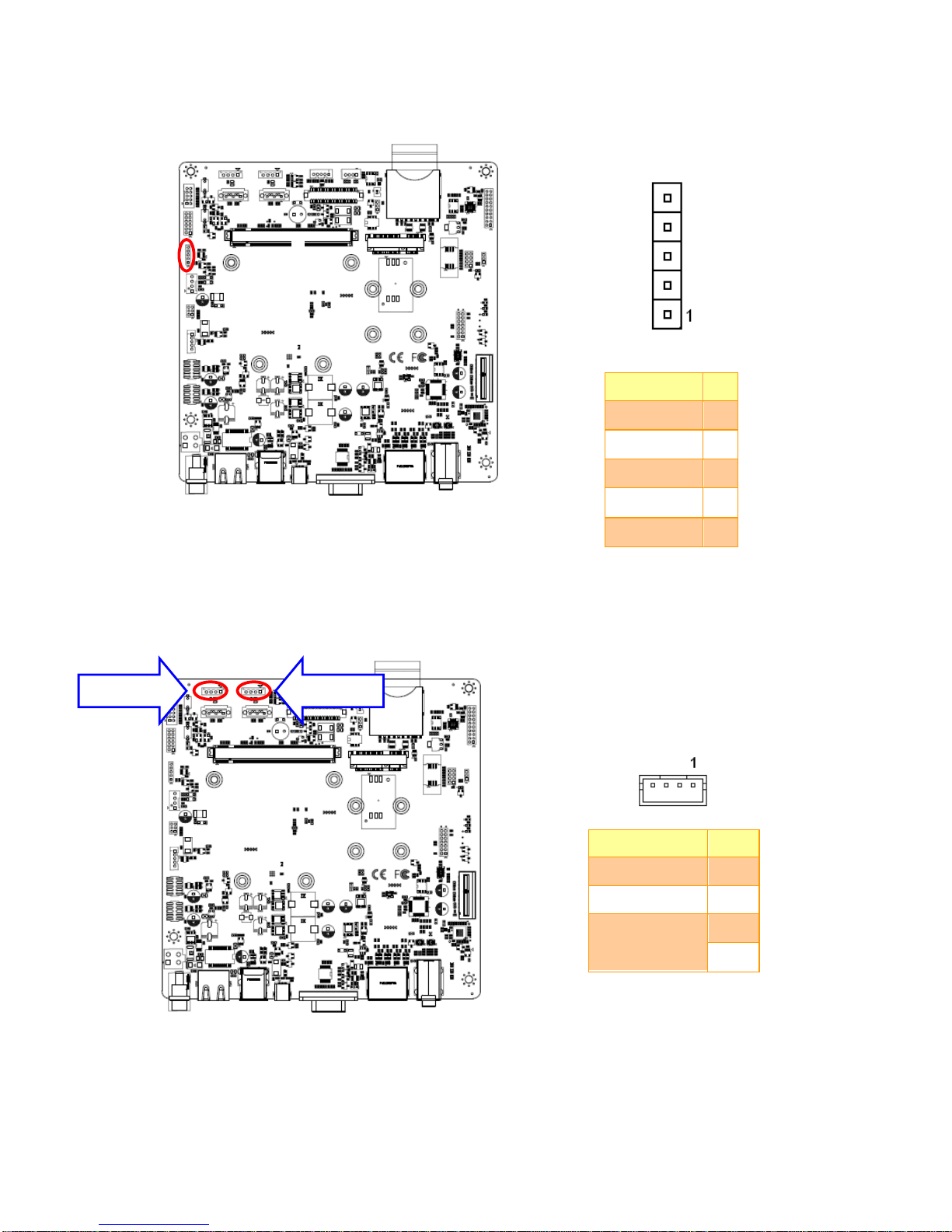
2.3.14 LCD Inverter connector (JBKLT1)
Signal
PIN
+12V
(max 300mA)
1
GND
2
LVDS_BPEN
3
LVDS_BKLTCTL
4
+5V
(max 400mA)
5
2.3.14.1 Signal Description – LCD Inverter connector (JBKLT)
Signal
Signal Description
LVDS_BKLTCTL
LVDS backlight PWM control
LVDS_BPEN
LCD backlight Enable/Disable control signal
LVDS_EN level
selectable resistor to 5V or 3.3V
(Default 5V level)
User’s Manual
REV-Q703 User’s Manual 23
2.3.15 Customer I2C connector (JI2C1)
Signal
PIN
GND
5
CS_DAT
4
CS_CLK
3
CS_INT#
2
+3.3V
1
2.3.16 HD Power connector 1/2 (HD_PWR1/2)
Signal
PIN
GND
1
GND
2
+5V
(Max 1000Ma)
3
4
HD_PWR1
HD_PWR2

REV-Q703
24 REV-Q703 User’s Manual
2.3.17 LVDS connector (JLVDS1)
Signal
PIN
PIN
Signal
+3V
1
2
+5V
+3V
3
4
+5V
QC_LVDS_DDC_CLK
5 6 QC_LVDS_DDC_DATA
GND
7
8
GND
LVDS_A1+
9
10
LVDS_A0+
LVDS_A1-
11
12
LVDS_A0-
GND
13
14
GND
LVDS_A3+
15
16
LVDS_A2+
LVDS_A3-
17
18
LVDS_A2-
GND
19
20
GND
LVDS_B1+
21
22
LVDS_B0+
LVDS_B1-
23
24
LVDS_B0-
GND
25
26
GND
LVDS_B3+
27
28
LVDS_B2+
LVDS_B3-
29
30
LVDS_B2-
GND
31
32
GND
LVDS_B_CLK+
33
34
LVDS_A_CLK+
LVDS_B_CLK-
35
36
LVDS_A_CLK-
GND
37
38
GND
+12V
39
40
+12V

User’s Manual
REV-Q703 User’s Manual 25
2.3.18 CAN Bus connector (JCAN1)
Signal
PIN
CAN0_H
1
GND
2
CAN0_L
3
GND
4
2.3.19 Battery connector (BAT-1)
Signal
PIN
+3.3V
1
GND
2

REV-Q703
26 REV-Q703 User’s Manual
4. Mechanical Drawing

User’s Manual
REV-Q703 User’s Manual 27
Unit: mm
 Loading...