


ERS-BYTE
Intel® Celeron® SoC Processor J1900 Fanless Rugged
Embedded System with 8 COM Isolations
Quick Reference Guide
1st Ed –23 March 2015
Copyright Notice
Copyright 2015 Avalue Technology Inc., ALL RIGHTS RESERVED.
Part No. E2017EA91A0R

ERS-BYTE
FCC Statement
Copyright Notice
Disclaimer
THIS DEVICE COMPLIES WITH PART 15 FCC RULES. OPERATION IS
SUBJECT TO THE FOLLOWING TWO CONDITIONS:
(1) THIS DEVICE MAY NOT CAUSE HARMFUL INTERFERENCE.
(2) THIS DEVICE MUST ACCEPT ANY INTERFERENCE RECEIVED INCLUDING
INTERFERENCE THAT MAY CAUSE UNDESIRED OPERATION.
THIS EQUIPMENT HAS BEEN TESTED AND FOUND TO COMPLY WITH THE LIMITS
FOR A CLASS "A" DIGITAL DEVICE, PURSUANT TO PART 15 OF THE FCC RULES.
THESE LIMITS ARE DESIGNED TO PROVIDE REASONABLE PROTECTION AGAINST
HARMFUL INTERFERENCE WHEN THE EQUIPMENT IS OPERATED IN A
COMMERCIAL ENVIRONMENT. THIS EQUIPMENT GENERATES, USES, AND CAN
RADIATE RADIO FREQUENCY ENERGY AND, IF NOT INSTALLED AND USED IN
ACCORDANCE WITH THE INSTRUCTION MANUAL, MAY CAUSE HARMFUL
INTERFERENCE TO RADIO COMMUNICATIONS.
OPERATION OF THIS EQUIPMENT IN A RESIDENTIAL AREA IS LIKELY TO CAUSE
HARMFUL INTERFERENCE IN WHICH CASE THE USER WILL BE REQUIRED TO
CORRECT THE INTERFERENCE AT HIS OWN EXPENSE.
Copyright 2015 Avalue Technology Inc., ALL RIGHTS RESERVED.
No part of this document may be reproduced, copied, translated, or transmitted in any form
or by any means, electronic or mechanical, for any purpose, without the prior written
permission of the original manufacturer.
Avalue Technology Inc. reserves the right to make changes, without notice, to any product,
including circuits and/or software described or contained in this manual in order to improve
design and/or performance. Avalue Technology assumes no responsibility or liability for the
use of the described product(s), conveys no license or title under any patent, copyright, or
masks work rights to these products, and makes no representations or warranties that
these products are free from patent, copyright, or mask work right infringement, unless
otherwise specified. Applications that are described in this manual are for illustration
purposes only. Avalue Technology Inc. makes no representation or warranty that such
application will be suitable for the specified use without further testing or modification.
2 ERS-BYTE Quick Reference Guide

Quick Reference Guide
3
CONTENT
1. Getting Started ............................................................................................................ 5
1.1 Safety Precautions ................................................................................................ 5
1.2 Packing List ........................................................................................................... 5
1.3 System Specifications ........................................................................................... 6
1.4 System Overview ................................................................................................... 8
1.4.1 Front View .................................................................................................................................... 8
1.4.2 Rear View ..................................................................................................................................... 8
1.5 System Dimensions ............................................................................................. 10
2. Hardware Configuration ........................................................................................... 11
2.1 ERS-BYTE connector mapping ........................................................................... 12
2.1.1 External Serial Port 1 connector (COM1) .................................................................................. 12
2.1.2 External Serial Port 3/4 connector (COM3/4) ............................................................................ 12
2.1.3 External Serial Port 5/6/7/8/9/10 connector (COM5/6/7/8/9/10) ................................................ 13
2.1.4 VGA connector (VGA) ................................................................................................................ 13
2.1.5 Multi-Function Port combined COM2, 2 PS/2, Audio, GPIO and SMBus (Multi-function port) . 14
2.1.5.1 GPIO+SMBUS ....................................................................................................................... 15
2.1.5.2 COM2 .................................................................................................................................... 15
2.2 EBM-BYTS and AUX-M03 Overviews ................................................................. 16
2.2.1 EBM-BYTS ................................................................................................................................. 16
2.2.2 AUX-M03 .................................................................................................................................... 17
2.3 EBM-BYTS Jumper & Connector list ................................................................... 17
2.4 EBM-BYTS Jumpers & Connectors settings ....................................................... 19
2.4.1 Clear CMOS (JCMOS1) ............................................................................................................. 19
2.4.2 COM 1/2 pin 9 signal select (JRI1/2) ......................................................................................... 19
2.4.3 AT/ ATX Input power select (JAT1) ........................................................................................... 20
2.4.4 LCD backlight brightness adjustment (JVR1) ............................................................................ 20
2.4.5 IET interface DP mode select (JDDI1) ....................................................................................... 21
2.4.6 UIM Switch select (JUIM1) ......................................................................................................... 21
2.4.7 Serial port 1/ 2 – RS485 mode select (SW1) ............................................................................. 22
2.4.8 LPC port connector (JLPC1) ...................................................................................................... 22
2.4.9 LCD inverter connector (JBKL1) ................................................................................................ 23
2.4.10 SPI connector (SPI1) ............................................................................................................. 23
2.4.11 Front Panel Connector 1 (CN1) ............................................................................................. 24
2.4.12 Front Panel Connector 2 (CN2) ............................................................................................. 24
2.4.13 DC Output connector (DCOUT_S1) ...................................................................................... 25
2.4.14 EC Debug connector (JEC_ROM1)....................................................................................... 25
ERS-BYTE Quick Reference Guide

ERS-BYTE
2.4.15 On-board header for USB2.0 (JUSB1) .................................................................................. 26
2.4.16 LVDS connector (JLVDS1) .................................................................................................... 26
2.5 AUX-M03 Connector list ...................................................................................... 27
2.6 AUX-M03 Connectors settings ............................................................................ 28
2.6.1 System reset (WCN1) ................................................................................................................ 28
2.6.2 LPT Port (WJPRT1) ................................................................................................................... 28
2.7 Installing Mounting Brackets (ERS-BYTE) .......................................................... 29
2.8 Installing Hard Disk & Memory, PCI devices (ERS-BYTE) .................................. 30
4 ERS-BYTE Quick Reference Guide

Quick Reference Guide
5
1. Getting Started
1.1 Safety Precautions
Warning!
Always completely disconnect the power cord from your
chassis whenever you work with the hardware. Do not
make connections while the power is on. Sensitive
electronic components can be damaged by sudden power
surges. Only experienced electronics personnel should
open the PC chassis.
Caution!
Always ground yourself to remove any static charge before
touching the CPU card. Modern electronic devices are very
sensitive to static electric charges. As a safety precaution,
use a grounding wrist strap at all times. Place all electronic
components in a static-dissipative surface or static-shielded
bag when they are not in the chassis.
1.2 Packing List
1 x ERS-BYTE Intel® Celeron® SoC Processor J1900 Fanless Rugged
Embedded System with 8 COM Isolations
1 x DVD-ROM contains the followings:
— User’s Manual (this manual in PDF file)
— Ethernet driver and utilities
— VGA drivers and utilities
— Audio drivers and utilities
Other major components include the followings:
— 44-Pin Multiple Function Cable
— Wall Mount Bracket
— Adapter
— Power Cord
— Screw kit for Wall Mount/Mini Card/2.5” Drive Bay
ERS-BYTE Quick Reference Guide
ERS-BYTE
System
Board
EBM-BYTS + AUX-M03
CPU
Intel® Celeron® J1900 2.0GHz Processor
BIOS
AMI uEFI BIOS, 64Mbit SPI Flash ROM
I/O Chip
EC ITE IT8528E
System Memory
1 x 204-Pin DDR3L 1333MHz SO-DIMM Socket Up to 8GB
Watchdog Timer
H/W Reset, 1sec. ~ 65535sec.
H/W Status Monitor
Monitoring CPU & System Temperature and Voltage
Storage
Solid State Drive
1 x 2.5” Drive Bay, 1 x mSATA
External I/O
COM Port
10 x RS-232 (COM1~COM4 can be set as 422/485 by BIOS);
COM3~COM10 supported 2.5KV Isolation
USB Port
5 x USB
Video Port
1 x VGA, 1 x LVDS
Audio Port
1 x Mic-In, 1 x Line-Out, 1 x Line-In
LAN Port
1 x RJ45
GPIO
6-bit GPI & 6-Bit GPO
Switch
1 x Power on/off
Indicator Light
1 x Power on/off LED
1 x Storage LED
Expansion Slots
2 x Mini PCIe (1 x mSATA supported)
Display
Chipset
Intel® Valleyview SoC integrated Graphics
Multiple Display
VGA
Resolution
VGA Mode: 2560 x 1080 @ 60Hz
Audio
HD Code
Realtek ALC892
Audio Interface
Mic-in, Line-in, Line-out
Ethernet
Chipset
Intel® I211AT Gigabit Ethernet Controller
Ethernet Interface
10/100/1000 Base-Tx Gigabit Ethernet Compatible
Environment & Mechanical
Power Type
+12 ~ +26Vdc (Lockable DC Jack)
ACPI
Single Power ATX Support S0, S3, S4, S5
ACPI 5.0 Compliant
1.3 System Specifications
6 ERS-BYTE Quick Reference Guide
Quick Reference Guide
7
Power Mode
AT/ ATX (ATX is The Default Setting)
Operating Temperature
-15°C ~ 60°C (5°F ~ 140°F) (w/CF & SSD), Ambient w/Air Flow
Storage Temperature
-40 ~ 75°C (-40 ~ 167°F)
Relative Humidity
0% ~ 90% Relative Humidity, Non-condensing
Vibration Protection
With CF/SSD: 5Grms, IEC 60068-2-64, Random, 10 ~ 500Hz,
1hr/axis
Shock Protection
With CF/SSD: 50G, IEC 60068-2-27, Half Sine,11ms
Certification
CE, FCC Class B
Dimension (W x D x H)
231mm x 160mm x 80mm
Weight
3.5Kgs
Color
Silver & Black
Fanless
Yes
Reliability
IP Rating
IP 30
Note: Specifications are subject to change without notice.
ERS-BYTE Quick Reference Guide
ERS-BYTE
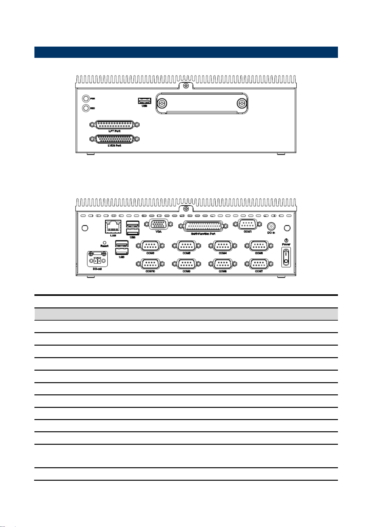
Connectors
Label
Function
Note
LPT Port
LPT connector
LVDS Port
LVDS connector
PWR
Power connector
HDD
HDD Indicator
USB
5 X USB connector
COM1
Serial port connector 1
COM3~10
Serial port connector 3~10
DC-In
DC power-in connector
DC-out
DC power-out connector
LAN
RJ-45 Ethernet
Multi-Function Port
Multi-Function Port combined COM2,
2 PS/2, Audio, GPIO and SMBus
VGA
VGA connector
1.4 System Overview
1.4.1 Front View
1.4.2 Rear View
8 ERS-BYTE Quick Reference Guide

9
Reset
Reset button
Power
Power-in connector
Quick Reference Guide
ERS-BYTE Quick Reference Guide

ERS-BYTE
(Unit: mm)
1.5 System Dimensions
10 ERS-BYTE Quick Reference Guide

11
2. Hardware
Configuration
Jumper and Connector Setting, Driver and BIOS Installing
For advanced information, please refer to:
1- EBM-BYTS and AUX-M03 included in this manual.
Note: If you need more information, please visit our website:
http://www.avalue.com.tw
Quick Reference Guide
ERS-BYTE Quick Reference Guide

ERS-BYTE
Pin
RS-232
RS-485
RS-422
1
DCD
TXD-/RXD-
TXD-
2
RXD
TXD+/RXD+
TXD+
3
TXD
RXD+
4
DTR
RXD-
5
GND
GND
GND
6
DSR 7 RTS 8 CTS 9 RI
Pin
RS-232
RS-485
RS-422
1
DCD
TXD-/RXD-
TXD-
2
RXD
TXD+/RXD+
TXD+
3
TXD
RXD+
4
DTR
RXD-
5
GND
GND
GND
6
DSR 7 RTS 8 CTS 9 RI
2.1 ERS-BYTE connector mapping
2.1.1 External Serial Port 1 connector (COM1)
2.1.2 External Serial Port 3/4 connector (COM3/4)
12 ERS-BYTE Quick Reference Guide

Quick Reference Guide
13
Signal
PIN
PIN
Signal
DCD
1 6 DSR
RXD
2 7 RTS
TXD
3 8 CTS
DTR
4 9 RI
GND
5
PIN
Signal
PIN
Signal
PIN
Signal
1
RED
6
GND
11
NC
2
GREEN
7
GND
12
DDCDAT
3
BLUE
8
GND
13
HSYNC
4
NC 9 +5V
14
VSYNS
5
GND
10
GND
15
DDCCLK
2.1.3 External Serial Port 5/6/7/8/9/10 connector (COM5/6/7/8/9/10)
2.1.4 VGA connector (VGA)
ERS-BYTE Quick Reference Guide

ERS-BYTE
PIN
Signal
PIN
Signal
PIN
Signal
1
LINE1_JD
16
FRONT_JD
31
LINE1_RIN
2
MIC1_JD
17
LINEOUT_R
32
GND
3
MIC_RIN
18
GND
33
LINE1_LIN
4
GND
19
LINEOUT_L
34
+5V
5
MIC_LIN
20
GND
35
DO3
6
DO5
21
DO4
36
DO0
7
DO2
22
DO1
37
DI3
8
DI5
23
DI4
38
DI0
9
DI2
24
DI1
39
SMB_CLK
10
MSCK
25
SMB_DATA
40
NRIB#
11
GND
26
GND
41
NRTSB#
12
MSDA
27
NCTSB#
42
COM2_GND
13
KBDA
28
NDSRB#
43
NTXDB_485RXP
14
VCC_PS2
29
NDTRB#_485RXN
44
NDCDB#_485TXN
15
KBCK
30
NRXDB_485TXP
2.1.5 Multi-Function Port combined COM2, 2 PS/2, Audio, GPIO and SMBus
(Multi-function port)
14 ERS-BYTE Quick Reference Guide

Quick Reference Guide
15
Signal
PIN
PIN
Signal
25
13
24
12
23
11
22
10 SMBUS_DATA
21 9
SMBUS_CLK
20 8 GND
GPI-D5
19 7 5V
GPI-D4
18 6 GPO-D5
GPI-D3
17 5 GPO-D4
GPI-D2
16 4 GPO-D3
GPI-D1
15 3 GPO-D2
GPI-D0
14 2 GPO-D1
1 GPO-D0
Pin
RS-232
RS-485
RS-422
1
DCD
TXD-/RXD-
TXD-
2
RXD
TXD+/RXD+
TXD+
3
TXD
RXD+
4
DTR
RXD-
5
GND
GND
GND
6
DSR
7
RTS
8
CTS 9 RI
2.1.5.1 GPIO+SMBUS
2.1.5.2 COM2
ERS-BYTE Quick Reference Guide

ERS-BYTE
2.2 EBM-BYTS and AUX-M03 Overviews
2.2.1 EBM-BYTS
16 ERS-BYTE Quick Reference Guide

17
Jumpers
Label
Function
Note
JCMOS1
Clear CMOS
3 x 1 header, pitch 2.54mm
JCMOS2
Clear CMOS (Reserved)
3 x 1 header, pitch 2.54 mm
JRI1/2
COM 1/2 pin 9 signal select
3 x 2 header, pitch 2.00 mm
JAT1
AT/ ATX Input power select
3 x 1 header, pitch 2.00 mm
SW1
Serial port 1/ 2 – RS485 mode select
DIP switch 6pin
JUIM1
UIM Switch select
3 x 1 header, pitch 2.00 mm
JVR1
LCD backlight brightness adjustment
3 x 1 header, pitch 2.00 mm
JDDI1
IET interface DP mode select
3 x 1 header, pitch 2.00 mm
2.2.2 AUX-M03
Quick Reference Guide
2.3 EBM-BYTS Jumper & Connector list
ERS-BYTE Quick Reference Guide

ERS-BYTE
Connectors
Label
Function
Note
USB_REAR
USB connector
USB_FRONT
USB connector
JUSB1
On-board header for USB2.0
5 x 1 header, pitch 2.00 mm
LAN1
LAN connector
VGA1
VGA connector
DB-1
Multi-function port
1. COM2
2. Audio(line-in, line-out,
mic-in)
3. 2 x PS/2 for KB/MS
4. 12 bit GPIO/SMBUS
COM1
Serial port connector 1
DCJACK1
DC-IN connector
MPCIE1/2
Mini PCI Express connector 1/2
52 pin
PWRBTN
Power button
RSTBTN
Reset button
LED_PWR
LED Power
LED_HD
LED HDD
LED_ACK
LED LAN
LED_SPD_LNK
LED LAN
SIMCARD1
SIM card slot
JLVDS1
LVDS connector
20 x 2 wafer, pitch 1.25 mm
SO_DIMM1
DDR3 SODIMM connector
MIOE_CB1
IET Expansion slot
JLPC1
LPC port connector
7 x 2 header, pitch 2.00 mm
SPI1
SPI connector
4 x 2 header, pitch 2.00 mm
JBKL1
LCD inverter connector
5 x 1 wafer, pitch 2.00 mm
SATA1
Serial ATA connector 1
CN1
Front Panel connector 1
5 x 1 wafer, pitch 2.00 mm
CN2
Front Panel connector 2
8 x 1 wafer, pitch 2.00 mm
DCOUT_S1
DC Output connector
6 x 1 wafer, pitch 2.00 mm
JEC_ROM1
EC Debug connector
5 x 2 header, pitch 2.00 mm
18 ERS-BYTE Quick Reference Guide

19
*Default
Protect*
Clear CMOS
* Default
Ring*
+5V
+12V
JRI1
JRI2
2.4 EBM-BYTS Jumpers & Connectors settings
2.4.1 Clear CMOS (JCMOS1)
Quick Reference Guide
2.4.2 COM 1/2 pin 9 signal select (JRI1/2)
ERS-BYTE Quick Reference Guide

ERS-BYTE
*Default
AT
ATX*
* Default
PWM Mode*
DC Mode
2.4.3 AT/ ATX Input power select (JAT1)
2.4.4 LCD backlight brightness adjustment (JVR1)
20 ERS-BYTE Quick Reference Guide

21
*Default
HDMI/DVI
Display Port*
* Default
UIM on MPCIE1
UIM on MPCIE2*
2.4.5 IET interface DP mode select (JDDI1)
Quick Reference Guide
2.4.6 UIM Switch select (JUIM1)
ERS-BYTE Quick Reference Guide

ERS-BYTE
In Serial Port 1 mode
ON
OFF
1
Auto Direction
RTS# Control*
2
485TXP external
biasing resistor
OPEN*
3
485TXN external
biasing resistor
OPEN*
In Serial Port 2 mode
ON
OFF
4
Auto Direction
RTS# Control*
5
485TXP external
biasing resistor
OPEN*
6
485TXN external
biasing resistor
OPEN*
Signal
PIN
PIN
Signal
LPC_AD0
1
2
+3.3V
LPC_AD1
3 4 LPC_PORT80_RST#
LPC_AD2
5 6 LPC_FRAME#
LPC_AD3
7 8 LPC1_PORT80_CLK
SERIRQ
9
10
GND
+5V
11
12
GND
+5VSB
13
14
NC
2.4.7 Serial port 1/ 2 – RS485 mode select (SW1)
2.4.8 LPC port connector (JLPC1)
22 ERS-BYTE Quick Reference Guide

23
Signal
PIN
+12V
1
GND
2
BKLEN
3
VBRIGHT
4
+5V
5
Signal
PIN
PIN
Signal
7 SPI_HOLD#
SPI_ROM_MOSI
6 5 SPI_ROM_MISO_R
SPI_ROM_CLK
4 3 SPI_ROM_CS#
GND
2 1 +VSPI_BIOS
2.4.9 LCD inverter connector (JBKL1)
Quick Reference Guide
2.4.10 SPI connector (SPI1)
ERS-BYTE Quick Reference Guide

ERS-BYTE
Signal
PIN
PWR_BTN_IN#
1
SYSRST#
2
GND
3
+5VSB
4
PWR_LED-
5
Signal
PIN
+3.3V
1
SATA_5V_LED#
2
+3.3VSB
3
LAN1_LED_ACT_n
4
+3.3VSB
5
LAN1_LED_100#_n
6
+3.3VSB
7
LAN1_LED_1000#_n
8
2.4.11 Front Panel Connector 1 (CN1)
2.4.12 Front Panel Connector 2 (CN2)
24 ERS-BYTE Quick Reference Guide

25
Signal
PIN
DC_OUT
1
DC_OUT
2
DC_OUT
3
GND
4
GND
5
GND
6
Signal
PIN
PIN
Signal
EC_SMDAT_DE
BUG
10
9
EC_SMCLK_D
EBUG
NC
8 7 EC_HOLD#
EC_FMOSI
6 5 EC_FMISO
EC_FSCK
4 3 EC_FSCE#
GND
2 1 +VSPI_EC
2.4.13 DC Output connector (DCOUT_S1)
Quick Reference Guide
2.4.14 EC Debug connector (JEC_ROM1)
ERS-BYTE Quick Reference Guide

ERS-BYTE
Signal
PIN
USBVCC_HEADER
1
USB_HUB2_DN_1
2
USB_HUB2_DP_1
3
GND
4
GND
5
Signal
PIN
PIN
Signal
+5V
2 1 +3.3V
+5V
4 3 +3.3V
NC
6
5
NC
GND
8 7 GND
LVDS_DATA0_P
10 9 LVDS_DATA1_P
LVDS_DATA0_N
12
11
LVDS_DATA1_N
GND
14
13
GND
LVDS_DATA2_P
16
15
LVDS_DATA3_P
LVDS_DATA2_N
18
17
LVDS_DATA3_N
GND
20
19
GND
LVDS_DATA4_P
22
21
LVDS_DATA5_P
LVDS_DATA4_N
24
23
LVDS_DATA5_N
GND
26
25
GND
LVDS_DATA6_P
28
27
LVDS_DATA7_P
LVDS_DATA6_N
30
29
LVDS_DATA7_N
GND
32
31
GND
LVDS_CLK1_P
34
33
LVDS_CLK2_P
LVDS_CLK1_N
36
35
LVDS_CLK2_N
GND
38
37
GND
+12V
40
39
+12V
2.4.15 On-board header for USB2.0 (JUSB1)
2.4.16 LVDS connector (JLVDS1)
26 ERS-BYTE Quick Reference Guide

27
Connectors
Label
Function
Note
WRSTBTN1
Reset button
WJPRT1
LPT Port
13 x 2 header, pitch 2.00mm
WCN1
System reset
2 x 1 wafer, pitch 2.50mm
WUSB_REAR
USB connector
COM3_7
Serial port connector 3 & 7
COM4_8
Serial port connector 4 & 8
COM5_9
Serial port connector 5 & 9
COM6_10
Serial port connector 6 & 10
WMIOE_IO
IET Expansion slot
2.5 AUX-M03 Connector list
Quick Reference Guide
ERS-BYTE Quick Reference Guide

ERS-BYTE
2.6 AUX-M03 Connectors settings
2.6.1 System reset (WCN1)
Signal
PIN
GND
2
WSYSRST#
1
2.6.2 LPT Port (WJPRT1)
Signal
PIN
PIN
Signal
GND
26
25
LPT_SLCT
GND
24
23
LPT_[E
GND
22
21
LPT_BUSY
GND
20
19
LPT_ACK#
GND
18
17
PD7
GND
16
15
PD6
GND
14
13
PD5
GND
12
11
PD4
GND
10 9 PD3
LPT_SLIN#
8 7 PD2
LPT_INIT#
6 5 PD1
LPT_ERR#
4 3 PD0
LPT_AFD#
2 1 STB-
28 ERS-BYTE Quick Reference Guide

29
2.7 Installing Mounting Brackets (ERS-BYTE)
Step 1. Locate brackets on both sides, matching the holes on the system.
Step 2. Insert and fasten 3 screws on each side of the system to secure Mounting brackets.
Quick Reference Guide
ERS-BYTE Quick Reference Guide

ERS-BYTE
Step 1. Remove 4 screws to release the HDD bracket.
Step 2.1. Slide HDD into its bracket until properly seated.
Step 2.2. Secure HDD by means of 4 screws.
Step 3. Remove 3 screws on each side of the system to release Mounting brackets and chassis cover.
Step 4. Insert the DDR3 SODIMM into the memory socket and fasten with the screw to complete DDR3 SODIMM
installation.
Step 5. Insert MPCIE cards into designated locations and fasten with 4 screws to complete MPCIE installation.
2.8 Installing Hard Disk & Memory, PCI devices (ERS-BYTE)
30 ERS-BYTE Quick Reference Guide
 Loading...