

Page 1

EEV-EX03
MicroATX ETX Carrier Board
Quick Installation Guide
1st Ed – 9 September 2009
Part No. E2017EX0300R
Page 2

EEV-EX03
FCC Statement
THIS DEVICE COMPLIES WITH PART 15 FCC RULES. OPERATION IS
SUBJECT TO THE FOLLOWING TWO CONDITIONS:
(1) THIS DEVICE MAY NOT CAUSE HARMFUL INTERFERENCE.
(2) THIS DEVICE MUST ACCEPT ANY INTERFERENCE RECEIVED INCLUDING
INTERFERENCE THAT MAY CAUSE UNDESIRED OPERATION.
THIS EQUIPMENT HAS BEEN TESTED AND FOUND TO COMPLY WITH THE LIMITS
FOR A CLASS "A" DIGITAL DEVICE, PURSUANT TO PART 15 OF THE FCC RULES.
THESE LIMITS ARE DESIGNED TO PROVIDE REASONABLE PROTECTION AGAINST
HARMFUL INTERFERENCE WHEN THE EQUIPMENT IS OPERATED IN A
COMMERCIAL ENVIRONMENT. THIS EQUIPMENT GENERATES, USES, AND CAN
RADIATE RADIO FREQUENCY ENERGY AND, IF NOT INSTATLLED AND USED IN
ACCORDANCE WITH THE INSTRUCTION MANUAL, MAY CAUSE HARMFUL
INTERFERENCE TO RADIO COMMUNICATIONS.
OPERATION OF THIS EQUIPMENT IN A RESIDENTIAL AREA IS LIKELY TO CAUSE
HARMFUL INTERFERENCE IN WHICH CASE THE USER WILL BE REQUIRED TO
CORRECT THE INTERFERENCE AT HIS OWN EXPENSE.
Notice
This guide is designed for experienced users to setup the system within the shortest time.
For detailed information, please always refer to the electronic user's manual.
Copyright Notice
Copyright 2009 Avalue Technology Inc., ALL RIGHTS RESERVED.
No part of this document may be reproduced, copied, translated, or transmitted in any form
or by any means, electronic or mechanical, for any purpose, without the prior written
permission of the original manufacturer.
Technical Support
We want you to get the maximum performance from your products. So if you run into
technical difficulties, we are here to help. For the most frequently asked questions, you can
easily find answers in your product documentation. These answers are normally a lot more
detailed than the ones we can give over the phone. So please consult the user’s manual
first.
To receive the latest version of the user’s manual; please visit our Web site at:
http://www.avalue.com.tw
2 EEV-EX03 Quick Installation Guide
Page 3

Quick Installation Guide
1. Getting Started
1.1 Safety Precautions
Warning!
Always completely disconnect the power cord from your
chassis whenever you work with the hardware. Do not
make connections while the power is on. Sensitive
electronic components can be damaged by sudden power
surges. Only experienced electronics personnel should
open the PC chassis.
Caution!
Always ground yourself to remove any static charge before
touching the CPU card. Modern electronic devices are very
sensitive to static electric charges. As a safety precaution,
use a grounding wrist strap at all times. Place all electronic
components in a static-dissipative surface or static-shielded
bag when they are not in the chassis.
1.2 Packing List
Before you begin installing your single board, please make sure that the
following materials have been shipped:
1 x EEV-EX03 ETX Carrier Board
1 x Quick Installation Guide
1 x CD-ROM or DVD-ROM contains the followings:
— User’s Manual (this manual in PDF file)
— Audio drivers and utilities
EEV-EX03 Quick Installation Guide 3
Page 4
EEV-EX03
2. Hardware
Configuration
4 EEV-EX03 Quick Installation Guide
Page 5
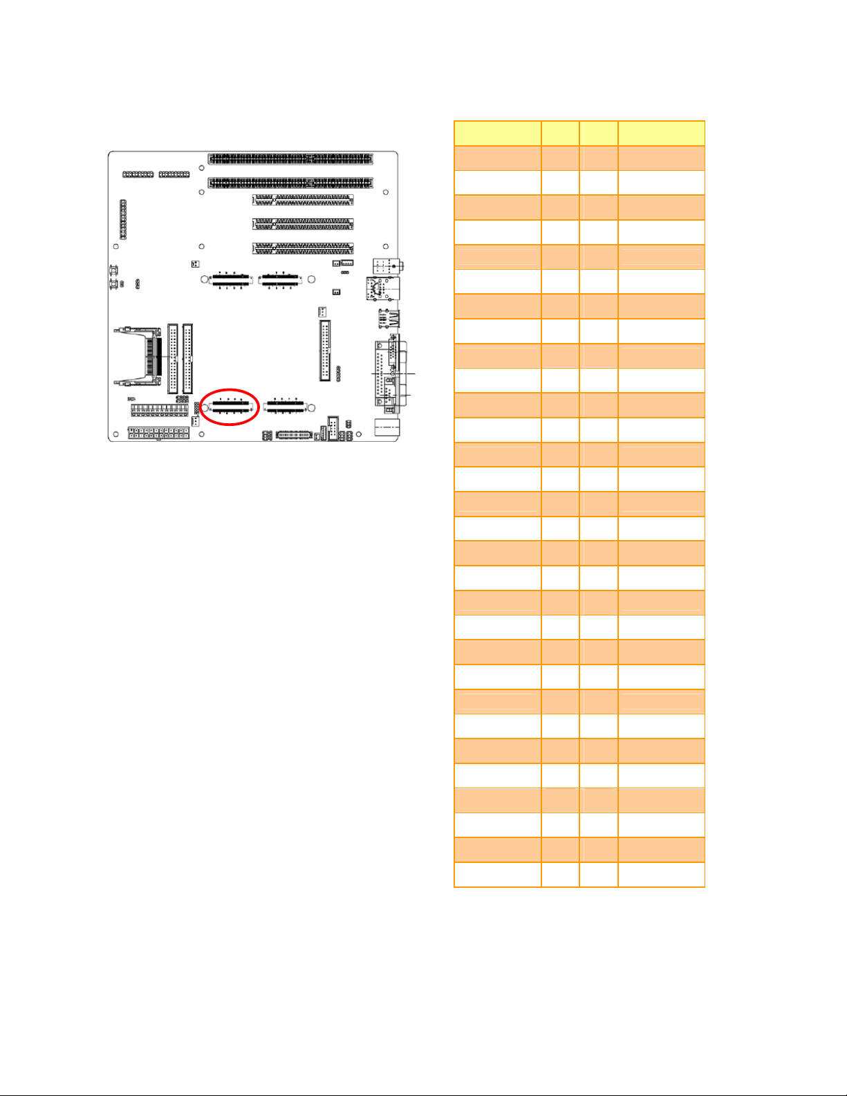
2.1 Product Overview
Quick Installation Guide
EEV-EX03 Quick Installation Guide 5
Page 6
EEV-EX03
2.2 Jumper and Connector List
You can configure your board to match the needs of your application by setting jumpers. A
jumper is the simplest kind of electric switch.
It consists of two metal pins and a small metal clip (often protected by a plastic cover) that
slides over the pins to connect them. To “close” a jumper you connect the pins with the clip.
To “open” a jumper you remove the clip. Sometimes a jumper will have three pins, labeled 1,
2, and 3. In this case, you would connect either two pins.
The jumper settings are schematically depicted in this manual as follows:
A pair of needle-nose pliers may be helpful when working with jumpers.
Connectors on the board are linked to external devices such as hard disk drives, a
keyboard, or floppy drives. In addition, the board has a number of jumpers that allow you to
configure your system to suit your application.
If you have any doubts about the best hardware configuration for your application, contact
your local distributor or sales representative before you make any changes.
The following tables list the function of each of the board's jumpers and connectors.
Jumpers
Label Function Note
J1
JFP1
J2
JP1
JP2
JP3
JP4
JRI2
6 EEV-EX03 Quick Installation Guide
MIC mode select 3 x 1 header, pitch 2.0mm
Miscellaneous setting connector 13 x 2 header, pitch 2.54mm
AT/ ATX mode select 2 x 1 header, pitch 2.54mm
Serial port 2 – RS232/422/485 mode select 3 x 2 header, pitch 2.54mm
(Reserved for BIOS programming) 3 x 1 header, pitch 2.54mm
Clear CMOS 3 x 1 header, pitch 2.54mm
Auto ATX power on 2 x 1 header, pitch 2.54mm
Serial port 2 pin 9 signal select 3 x 2 header, pitch 2.54mm
Page 7

Connectors
Label Function Note
Quick Installation Guide
AT1
ATX1
CF1
CN1-1
CN1-2
CN1-3
CN2
CN3-1
CN3-2
CN4
CN5
CN6
CN7
CN8
CPUFAN1
ETX1/2/3/4
AT Power connector 12x 1 header, pitch 3.96mm
ATX Power connector 12 x 2 header, pitch 4.2mm
Compact Flash card connector
Print port D-sub 25-pin, female
COM1 connector D-sub 9-pin, male
VGA connector D-sub 15-pin, female
USB connector 2&3 Double deck
LAN port connector
USB connector 0 & 1
Audio connector
AMP Right Out connector 2 x 1 wafer, pitch 2.0mm
AMP Left Out connector 2 x 1 wafer, pitch 2.0mm
SMCLK/ SMDAT connector 4 x 1 header, pitch 2.54mm
I2CLK/ I2DAT connector 4 x 1 header, pitch 2.54mm
CPU fan connector 3 x 1 wafer, pitch 2.54mm
ETX connector 1/2/3/4
FAN1
FAN2
FLP1
IDE1
IDE2
ISA1
ISA2
JBKL1
JBKL2
JCD1
JCOM2
JDIO1
JDIO2
JIR1
JLVDS1
JRS422/1
System fan connector 3 x 1 wafer, pitch 2.54mm
System fan connector 2 x 1 wafer, pitch 2.54mm
Floppy connector 17 x 2 header, pitch 2.54mm
Primary IDE connector 20 x 2 header, pitch 2.54mm
Primary IDE connector 20 x 2 header, pitch 2.54mm
ISA BUS connector 1 49 x 2 header, pitch 2.54mm
ISA BUS connector 2 49 x 2 header, pitch 2.54mm
LCD inverter connector
LCD inverter connector 4 x 1 wafer, pitch 2.0mm
CD-ROM audio connector
Serial Port 2 in RS-232 mode connector
General purpose I/O connector 10 x 2 header, pitch 2.54mm
General purpose I/O connector 10 x 2 header, pitch 2.54mm
IrDA connector 5 x 1 header, pitch 2.54mm
LVDS connector DIN 40-pin wafer, pitch1.25mm
Serial Port 2 in RS-422/485 mode 3 x 2 header, pitch 2.54mm
5 x 1 wafer, pitch 2.0mm
4 x 1 wafer, pitch 2.0mm
5 x 2 header, pitch 2.54mm
JTV1
KB_MS1
TV out connector 3 x 2 header, pitch 2.54mm
PS/2 keyboard & mouse connector
EEV-EX03 Quick Installation Guide 7
Page 8

EEV-EX03
PCI1
PCI slot 1
PCI2
PCI3
PWRBTN1
RESET1
PCI slot 2
PCI slot 3
Power button connector
Reset button connector
8 EEV-EX03 Quick Installation Guide
Page 9
2.3 Setting Jumpers & Connectors
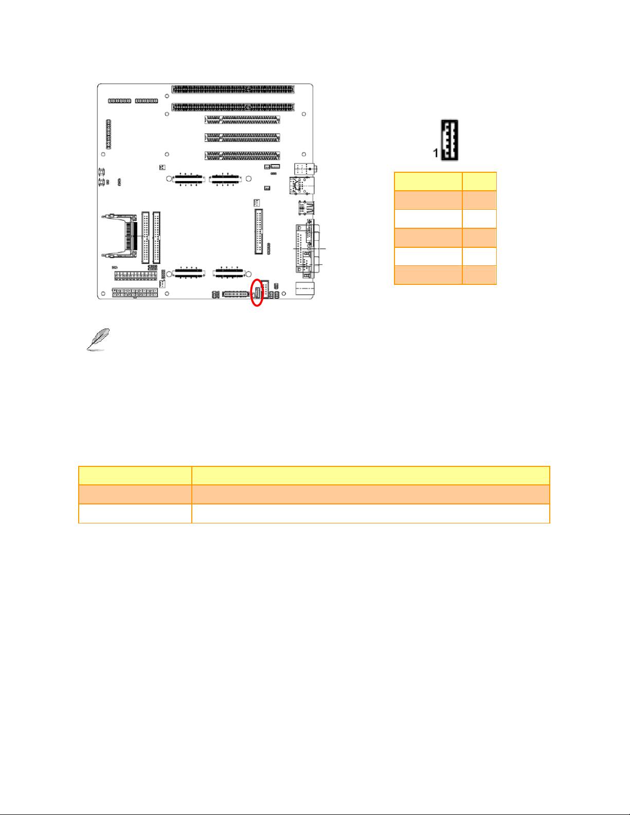
2.3.1 MIC mode select (J1)
*Default
Quick Installation Guide
Center*
2.25V Ref
2.3.2 AT/ATX mode select (J2)
* Default
AT*
ATX
EEV-EX03 Quick Installation Guide 9
Page 10
EEV-EX03
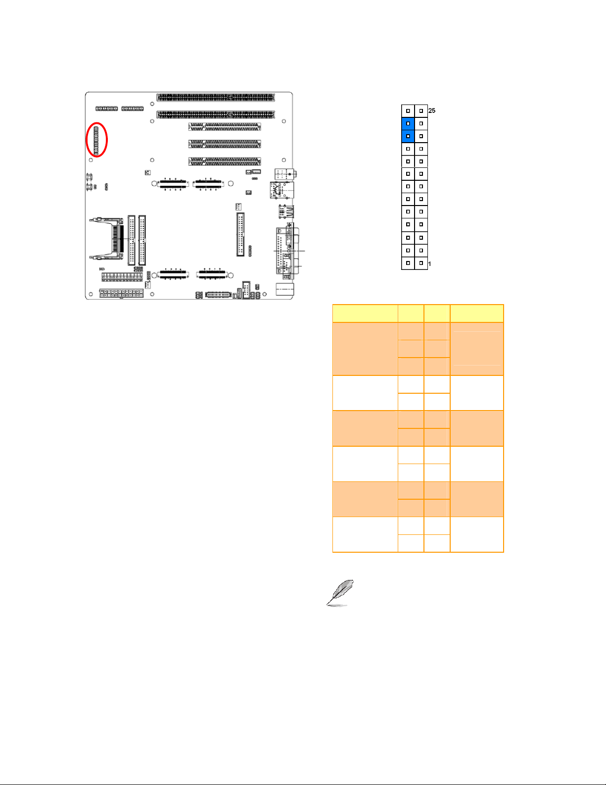
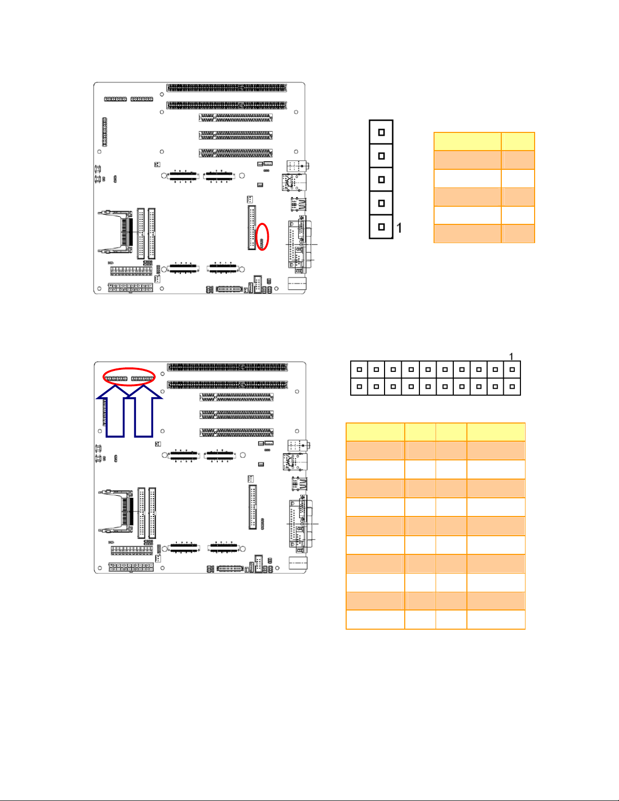
2.3.3 Miscellaneous setting connector (JFP1)
*Default
Master*
Signal PIN PIN Signal
CF Set
NC
26 25
24 23
22 21
20 19
18 17
LVDS
BRIGHT
NC
External
SPEAK
NC
LED
LED
16 15
14 13
12 11
10 9
8 7 POWER ON
6 5
4 3 STANDBY
2 1
KB LOCK
POWER
BUTTON
IDE LED
RESET
Note: To set the CF Card as Master ,
please short JFP1 pin 24 & 26
10 EEV-EX03 Quick Installation Guide
Page 11
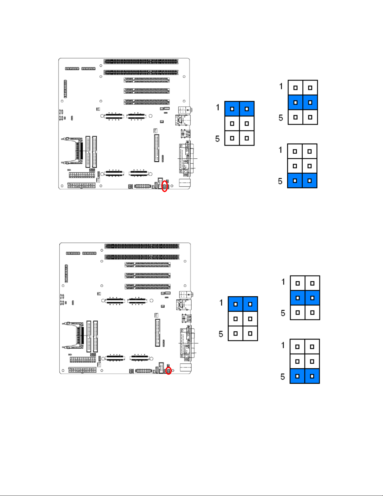
2.3.4 Serial port 2 RS232/422/485 mode select (JP1)
RS232*
Quick Installation Guide
RS422
RS485
* Default
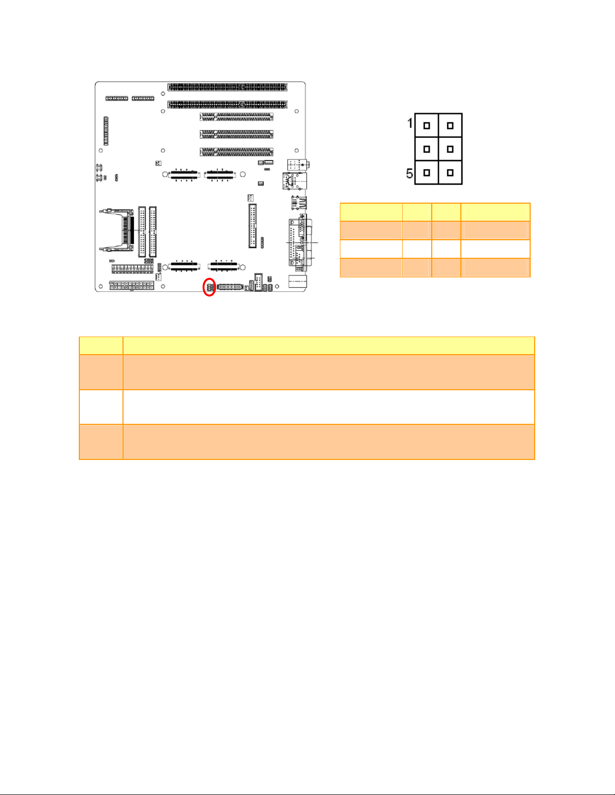
2.3.5 Serial port 2 pin 9 signal select (JRI2)
Ring*
+5V
+12V
* Default
EEV-EX03 Quick Installation Guide 11
Page 12
EEV-EX03
2.3.6 Serial Port 2 in RS-232 mode connector (JCOM2)
Signal PIN PIN
RI2 9 10 NC
RTS2 7 8 CTS2
GND 5 6 DSR2
TXDD2 3 4 DTR2
DCD2 1 2 RXDD2
Signal
JP1
Note:
12 EEV-EX03 Quick Installation Guide
When JP1 is in RS-422/482 mode, JCOM2 is
inaction.
Page 13

2.3.7 Serial Port 2 in RS-422/485 mode (JRS422/1)
Quick Installation Guide
In 422 mode
Signal PIN PIN
TX- 1 2 RX-
TX+ 3 4 RX+
+5V 5 6 GND
Signal
JP1
In 485 mode
Signal PIN PIN
DATA- 1 2 NC
Signal
DATA+ 3 4 NC
+5V 5 6 GND
JP1
EEV-EX03 Quick Installation Guide 13
Page 14

EEV-EX03
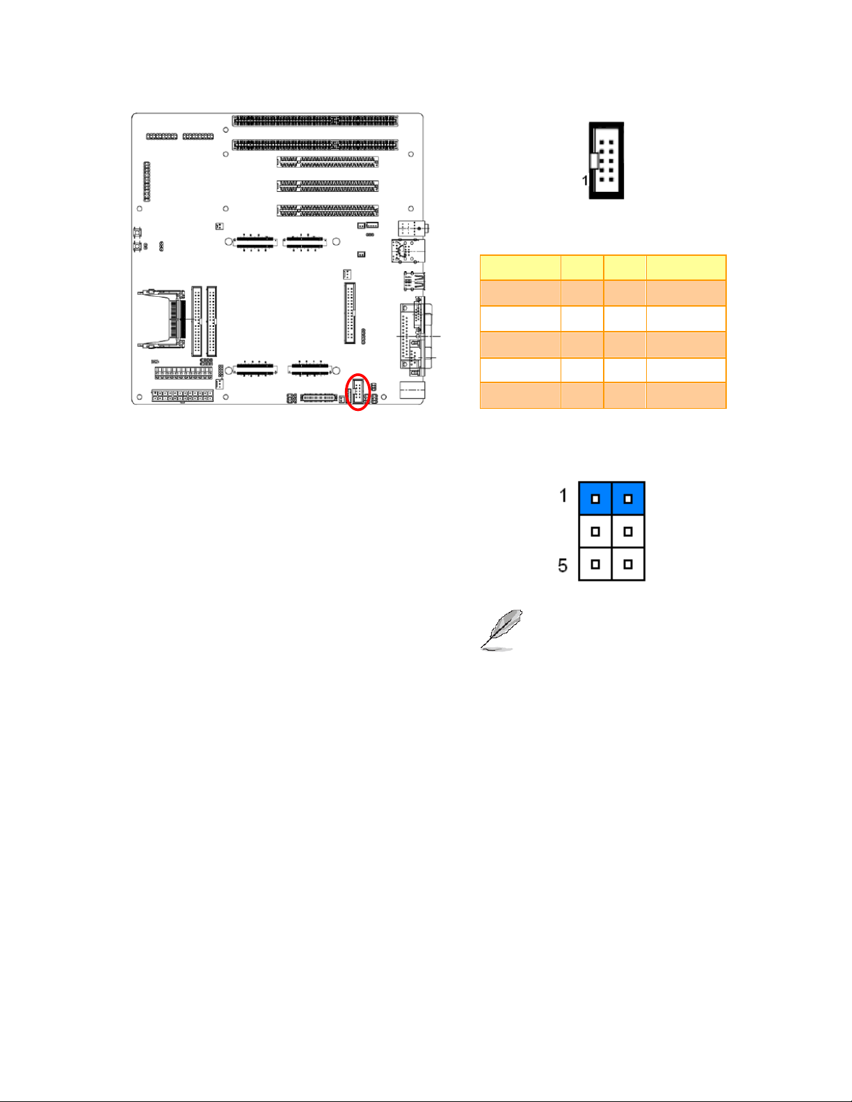
2.3.8 Clear CMOS (JP3)
* Default
Protect*
Clear CMOS
2.3.9 Auto ATX power on (JP4)
* Default
Close
Open*
14 EEV-EX03 Quick Installation Guide
Page 15

2.3.10 AT Power Connector (AT1)
Quick Installation Guide
Signal PIN
PWROK 1
+5V 2
+12V 3
-12V 4
GND 5
GND 6
GND 7
2.3.11 ATX Power Connector (ATX1)
GND 8
-5V 9
+5V 10
+5V 11
+5V 12
Signal PIN PIN Signal
+3.3V 1 13
+3.3V 2 14
GND 3 15
+5V 4 16 PS_ON
GND 5 17
+3.3V
-12V
GND
GND
+5V 6 18
GND 7 19
PWROK 8 20
AUX5V 9 21
+12V 10 22
+12V 11 23
+3.3V 12 24
GND
GND
-5V
+5V
+5V
+5V
GND
EEV-EX03 Quick Installation Guide 15
Page 16

EEV-EX03
2.3.12 AMP Right/ Left out connector (CN5/ CN6)
CN6
CN5
2.3.13 SMBCLK/ SMBDAT connector (CN7)
Signal PIN
AMP_ROUT+/ AMP_LOUT+ 1
AMP_ROUT-/ AMP_LOUT- 2
CN7
CN8
16 EEV-EX03 Quick Installation Guide
Signal PIN
+5V 1
SMBCLK 2
SMBDAT 3
GND 4
Page 17

2.3.14 I2CLK/ I2DAT connector (CN8)
Quick Installation Guide
Signal PIN
+5V 1
CN7
CN8
2.3.15 CPU Fan connector (CPUFAN1)
12CLK 2
12DAT 3
GND 4
Signal PIN
GND 1
+12V 2
NC 3
EEV-EX03 Quick Installation Guide 17
Page 18

EEV-EX03
2.3.16 System fan connector (FAN1/FAN2)
FAN2
FAN1
2.3.17 CD-ROM Audio Connector (JCD1)
Signal PIN
GND 1
+12V 2
NC 3
Signal PIN
GND+ 1
5V 2
18 EEV-EX03 Quick Installation Guide
Signal PIN
GND 1
LINEL 2
GND 3
LINER 4
Page 19
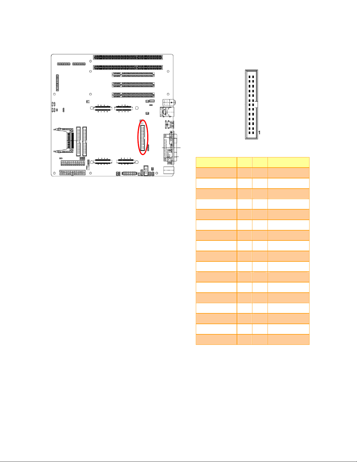
2.3.18 Floppy connector (FLP1)
Quick Installation Guide
Signal PIN PIN
GND 1 2 REDWC
GND 3 4 NC
NC 5 6 NC
GND 7 8 INDEX
GND 9 10
GND 11 12
GND 13 14
GND 15 16
GND 17 18
GND 19 20
GND 21 22
GND 23 24
GND 25 26
GND 27 28
GND 29 30
GND 31 32
Signal
MOTSA
DRVSB
DRVSA
MOTEB
DIR
STEP
WDATA
WGATE
TK00
WPT
RDATA
SIDE1
GND 33 34
DSKCHG
EEV-EX03 Quick Installation Guide 19
Page 20

EEV-EX03
IDE2
2.3.19 Primary IDE Connector (IDE1/IDE2)
IDE1
Signal PIN PIN
HDRST 1 2
HQ7/HP7 3 4
HQ6/HP6 5 6
HQ5/HP5 7 8
HQ4/HP4 9 10
HQ3/HP3 11 12
HQ2/HP2 13 14
HQ1/HP1 15 16
HQ0/HP0 17 18
GND 19 20
QDREQ/HDREQ 21 22
QIOW/HDIOW 23 24
QIOR/HDIOR 25 26
QIRDY/HIORDY 27 28
Signal
GND
HQ8/HP8
HQ9/HP9
HQ10/HP10
HQ11/HP11
HQ12/HP12
HQ13/HP13
HQ14/HP14
HQ15/HP15
GND
GND
GND
GND
20 EEV-EX03 Quick Installation Guide
QDACK/HDACK 29 30
QIRQ/HIRQ 31 32
QDA1/HDA1 33 34 SPDIAG_S/DMA100
QDA0/HDA0 35 36
QDCS1/HCS#1 37 38
HD_LED2/HD_LED1 39 40
GND
NC
QDA2/HDA2
QDCS3/HCS#3
GND
Page 21

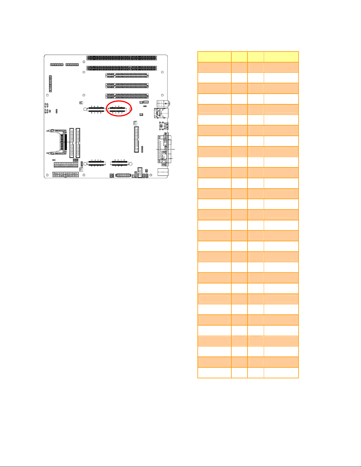
2.3.20 LVDS connector (JLVDS1)
Quick Installation Guide
Signal PIN PIN
+5V 2 1 +3.3V
+5V 4 3 +3.3V
SPDATA 6 5 SPCLK
GND 8 7 GND
YA0P 10 9 YA1P
YA0M 12 11 YA1M
GND 14 13 GND
YA2P 16 15 YA3P
YA2M 18 17 YA3M
GND 20 19 GND
YA6P 22 21 YA5P
YA6M 24 23 YA5M
GND 26 25 GND
YA8P 28 27 YA7P
YA8M 30 29 YA7M
Signal
Note:
Please notice that there are limitations of output current.
Max current output: 5V@ 3A, 3.3V@ 3V, 12V@ 3V
2.3.21 LCD Inverter Connector (JBKL2)
GND 32 31 GND
CLK1P 34 33 CLK2P
CLK1M 36 35 CLK2M
GND 38 37 GND
+12V 40 39 +12V
Signal PIN
GND 2
B12V 1
Note:
Please notice that there are limitations of output
current. Max current output: 12V@ 1.5V
EEV-EX03 Quick Installation Guide 21
Page 22
EEV-EX03
2.3.22 LCD Inverter Connector (JBKL1)
Signal PIN
+12V 1
GND 2
ENBKL 3
VR 4
+5V 5
Note:
Please notice that there are limitations of output current. Max current output: 12V@ 1.5V
For inverters with adjustable Backlight function, it is possible to control the LCD brightness through the
VR signal controlled by JFP1 Pin 21/23/25. Please see the JFP1 section for detailed circuitry
information.
2.3.22.1 Signal Description – LCD Inverter Connector (JBKL1)
Signal Signal Description
VR Vadj = 0.75V ~ 4.25V (Recommended: 4.7KΩ, >1/16W)
ENBKL LCD backlight ON/OFF control signal
22 EEV-EX03 Quick Installation Guide
Page 23
2.3.23 IrDA Connector (JIR1)
Quick Installation Guide
Signal PIN
IRTX 5
GND 4
IRRX 3
NC 2
2.3.24 General Purpose I/O Connector (JDIO1/JDIO2)
JDIO1
JDIO2
Signal PIN PIN
DIO0/GPO0 1 2 DIO10/GPI0
DIO1/GPO1 3 4 DIO11/GPI1
DIO2/GPO2 5 6 DIO12/GPI2
DIO3/GPO3 7 8 DIO13/GPI3
DIO4/GPO4 9 10 DIO14/GPI4
+5V 1
Signal
DIO5/GPO5 11 12 DIO15/GPI5
DIO6/GPO6 13 14 DIO16/GPI6
DIO7/GPO7 15 16 DIO17/GPI7
SMBCLK 17 18 SMBDAT
GND 19 20 +5V
EEV-EX03 Quick Installation Guide 23
Page 24
EEV-EX03
2.3.25 TV Out Connector (JTV1)
Signal PIN PIN
CVBS_OUT 1 2 GND
Y_OUT 3 4 C_OUT
GND 5 6 GND
2.3.25.1 Signal Description – TV Out Connecter (JTV1)
Signal
TVDAC Channel A Output: supports CVBS signal of Composite; Chrominance (Pb) analog signal
Pb
of Component.
TVDAC Channel B Output: supports Luminance signal of S-Video; Luminance (Y) analog signal
Y
of Component.
TVDAC Channel C Output: supports Chrominance analog signal of S-Video; Chrominance (Pr)
Pr
analog signal of Component.
Description
Signal
24 EEV-EX03 Quick Installation Guide
Page 25
2.3.26 ETX Connector 1 (ETX1)
A3 A4
A7 A8
Quick Installation Guide
Signal PIN PIN
GND A1 A2
PCICLK3
GND A5 A6
PCICLK1
REQ#3 A9 A10 GNT#3
GNT#2
REQ#2 A13 A14 GNT#1
REQ#1
GNT#0 A17 A18
+5V
SERIRQ A21 A22 REQ#0
AD0
AD1 A25 A26
AD4
AD6 A29 A30
CBE#0
A11 A12
A15 A16
A19 A20
A23 A24
A27 A28
A31 A32
Signal
GND
PCICLK4
GND
PCICLK2
+3V
+3V
NC
+5V
+3V
AD2
AD3
AD5
AD7
AD8 A33 A34
GND
AD10 A37 A38 AUXAL
AD11
AD12 A41 A42 AUXAR
AD13
AD14 A45 A46
AD15
CBE#1 A49 A50
+5V
PAR A53 A54 SERR#
PERR#
PME# A57 A58
LOCK#
A35 A36
A39 A40
A43 A44
A47 A48
A51 A52
A55 A56
A59 A60
AD9
GND
MIC
ASVCC
SNDL
ASGND
SNDR
+5V
NC
USB2-
DEVSEL#
EEV-EX03 Quick Installation Guide 25
Page 26

EEV-EX03
Signal PIN PIN
TRDY# A61 A62
Signal
USB3-
IRDY#
FRAME# A65 A66
GND
AD16 A69 A70
AD17
AD19 A73 A74
AD20
AD22 A77 A78
AD23
AD24 A81 A82
+5V
AD25 A85 A86
AD28
AD27 A89 A90
AD30
PCIRST# A93 A94
INTR#C
A63 A64
A67 A68
A71 A72
A75 A76
A79 A80
A83 A84
A87 A88
A91 A92
A95 A96
STOP#
USB2+
GND
CBE#2
USB3+
AD18
USB0-
AD21
USB1-
CBE#3
+5V
AD26
USB0+
AD29
USB1+
AD31
INTR#D
INTR#A A97 A98
GND
A99 A100
INTR#B
GND
2.3.27 Signal Description – ETX Connector 1 (ETX1)
2.3.27.1 PCI Signals
Signal Signal Description
PCI clock outputs for up to 4 external PCI slots or devices.
PCICLK [1:4]
REQ [0:3]#
GNT [0:3]#
AD [0:31]
CBE [0:3]#
PAR
SERR#
PERR# Parity Error. For PCI operation per exception granted by PCI 2.1 Specification.
The baseboard designer should route these clocks for 1300pS total delay from the
ETX connector pin to the clock pin of the PCI device. See the ETX Design Guide
for typical route length calculations.
Bus Request signals for up to 4 external bus mastering PCI devices. When
asserted, a PCI device is requesting PCI bus ownership from the arbiter.
Grant signals to PCI Masters. When asserted by the arbiter, the PCI master has
been granted ownership of the PCI bus.
PCI Address and Data Bus Lines. These lines carry the address and data
information for PCI transactions.
PCI Bus Command and Byte Enables. Bus command and byte enables are
multiplexed in these lines for address and data phases, respectively.
Parity bit for the PCI bus. Generated as even parity across AD [31:0] and CBE
[3:0]#.
System Error. Asserted for hardware error conditions such as parity errors
detected in DRAM.
26 EEV-EX03 Quick Installation Guide
Page 27

LOCK#
DEVSEL#
TRDY#
IRDY#
STOP#
FRAME#
PCIRST#
INTRA#,
INTRB#,
INTRC#,
INTRD#
IDSEL
PME# Power management event.
Lock Resource Signal. This pin indicates that either the PCI master or the bridge
intends to run exclusive transfers.
Device Select. When the target device has decoded the address as its own cycle,
it will assert DEVSEL#.
Target Ready. This pin indicates that the target is ready to complete the current
data phase of a transaction.
Initiator Ready. This signal indicates that the initiator is ready to complete the
current data phase of a transaction.
Stop. This signal indicates that the target is requesting that the master stop the
current transaction.
Cycle Frame of PCI Buses. This indicates the beginning and duration of a PCI
access. The access will be either an output driven by the Northbridge on behalf of
the CPU, or an input during PCI master access.
PCI Bus Reset. This is an output signal to reset the entire PCI Bus. This signal is
asserted during system reset.
PCI interrupts.
These interrupts are sharable and are typically wired in rotation to PCI slots or
devices.
This pin is not present on the EEV-EX03 module connector, but it is present on
each PCI slot connector or device. IDSEL is an input to the device that is used to
set the device’s configuration address for PCI configuration cycles. The IDSEL pin
of each device is typically connected to one of the AD lines in order to set a unique
configuration address.
In ETX systems, the four external bus slots or devices are assumed to use
AD[19:22] for IDSEL connections.
Quick Installation Guide
2.3.27.2 Audio Signals
Signal Signal Description
Line-level stereo output left/ right. These outputs have a nominal level of 1 volt
SNDL/ SNDR
AUXAL/ AUXAR
MIC
ASGND
ASVCC
RMS into a 10K impedance load. These outputs cannot drive low-impedance
speakers directly.
Auxiliary A input left/ right. Normally intended for connection to an internal or
external CDROM analog output or a similar line-level audio source. Minimum input
impedance is 5KOhm.
Nominal input level is 1 volt RMS.
Microphone input. Minimum input impedance is 5KOhm, max. Input voltage is 0.15
Vp-p.
Analog ground for sound controller. Use this signal ground for an external amplifier
in order to achieve lowest audio noise levels.
Analog supply voltage for sound controller. This is an output which is used for
production test only. Do not make external connections to this pin.
2.3.27.3 USB Signals
Signal Signal Description
USB [0:3]
USB [0:3]-
Universal Serial Bus Port [0:3] positive signal.
These are the serial data pairs for USB Port N-and Port N#.
Universal Serial Bus Port [0:3] negative signal.
These are the serial data pairs for USB Port N-and Port N#.
EEV-EX03 Quick Installation Guide 27
Page 28

EEV-EX03
2.3.28 ETX Connector 2 (ETX2)
Signal PIN PIN
Signal
GND B1 B2
SD14
SD13 B5 B6 MASTER#
SD12
SD11 B9 B10 DACK#7
SD10
SD9 B13 B14 DACK#6
SD8
MEMW# B17 B18 DACK#5
MEMR#
LA17 B21 B22 DACK#0
LA18
LA19 B25 B26
LA20
LA21 B29 B30
LA22
LA23 B33 B34
B3 B4
B7 B8
B11 B12
B15 B16
B19 B20
B23 B24
B27 B28
B31 B32
GND
SD15
DREQ7
DREQ6
DREQ5
DREQ0
IRQ14
IRQ15
IRQ12
IRQ11
IRQ10
IO16#
GND
SBHE# B37 B38
SA0
SA1 B41 B42
SA2
SA3 B45 B46 DACK#2
SA4
SA5 B49 B50
+5V
SA7 B53 B54
SA8
SA9 B57 B58
SA10
B35 B36
B39 B40
B43 B44
B47 B48
B51 B52
B55 B56
B59 B60
GND
M16#
OSC
BALE
TC
IRQ3
IRQ4
+5V
IRQ5
IRQ6
IRQ7
SYSCLK
28 EEV-EX03 Quick Installation Guide
Page 29

Quick Installation Guide
Signal PIN PIN
SA10 B61 B62 REFCH#
Signal
SA11
SA12 B65 B66 DACK#1
GND
SA13 B69 B70
SA14
SA15 B73 B74
SA16
SA18 B77 B78
SA19
IOCHRDY B81 B82
+5V
SD0 B85 B86 SMEMW#
SD2
SD3 B89 B90
DREQ2
SD5 B93 B94
SD6
B63 B64
B67 B68
B71 B72
B75 B76
B79 B80
B83 B84
B87 B88
B91 B92
B95 B96
DREQ1
GND
DREQ3
DACK#3
IOR#
IOW#
SA17
SMEMR#
AEN
+5V
SD1
NOWS#
SD4
IRQ9
SD7
IOCHK# B97 B98 RSTDRV
2.3.29 Signal Description – ETX Connector 2 (ETX2)
2.3.29.1 ISA Signals
Signal Signal Description
These signals provide data bus bits 0 to 15 for any peripheral devices. All 8-bit
devices use SD[0:7] for data transfers. 16-bit devices use SD[0:15].
SD[0:15]
SA[0:19]
SBHE#
BALE
AEN
To support 8-bit devices, the data on SD[8:15] is gated to SD[0:7] during 8-bit
transfers to these devices. 16-bit CPU cycles will be automatically converted into
two 8-bit cycles for 8-bit peripherals.
Address bits 0 through 15 are used to address I/O devices. Address bits 0 through
19 are used to address memory within the system. These 20 address lines, in
addition to LA[17:23] allow access of up to 16MB of memory. SA[0:19] are gated
on the ISA-bus when BALE is high and latched on to the falling edge of BALE.
Bus High Enable indicates a data transfer on the upper byte of the data bus
SD[8:15]. 16-bit I/O devices use SBHE# to enable data bus buffers on SD[8:15].
BALE is an active-high pulse generated at the beginning of any bus cycle initiated
by a CPU module. It indicates when the SA[0:19], LA17.23, AEN, and SBHE#
signals are valid.
AEN is an active-high output that indicates a DMA transfer cycle. Only resources
with a active DACK# signal should respond to the command lines when AEN is
high.
GND
B99 B100
GND
EEV-EX03 Quick Installation Guide 29
Page 30

EEV-EX03
MEMR#
SMEMR#
MEMW#
SMEMW#
IOR#
IOW#
IOCHK#
IOCHRDY
M16#
IO16#
REFSH#
NOWS#
MASTER#
SYSCLK
OSC
RESETDRV
DREQ
[0, 1, 2, 3, 5, 6, 7]
MEMR# instructs memory devices to drive data onto the data bus. MEMR# is
active for all memory read cycles.
SMEMR# instructs memory devices to drive data onto the data bus. SMEMR# is
active for memory read cycles to addresses below 1MB.
MEMW# instructs memory devices to store the data present on the data bus.
MEMW# is active for all memory write cycles.
SMEMW# instructs memory devices to store the data present on the data bus.
SMEMW# is active for all memory write cycles to address below 1MB.
I/O read instructs an I/O device to drive its data onto the data bus. It may be driven
by the CPU or by the DMA controller. IOR# is inactive (high) during refresh cycles.
I/O write instructs an I/O device to store the data present on the data bus. It may be
driven by the CPU or by the DMA controller. IOW# is inactive (high) during refresh
cycles.
IOCHK# is an active-low input signal that indicates that an error has occurred on
the module bus. If I/O checking is enabled on the CPU module, an IOCHK#
assertion by a peripheral device sends a NMI to the processor.
The I/O Channel Ready is pulled low in order to extend the read or write cycles of
any bus access when required. The CPU, DMA controllers or refresh controller can
initiate the cycle.
Any peripheral that cannot present read data or strobe in write data within this
amount of time use IOCHRDY to extend these cycles.
This signal should not be held low for more than 2.5 µs for normal operation. Any
extension to more than 2.5 µs does not guarantee proper DRAM memory content
due to the fact that memory refresh is disabled while IOCHRDY is low.
The M16# signal determines when a 16-bit to 8-bit conversion is needed for
memory bus cycles. A conversion is done any time the CPU module requests a
16-bit memory cycle while the M16# line is high. If M16# is high, 16-bit CPU cycles
are automatically converted on the bus into two 8-bit cycles. If M16# is low, an
access to peripherals is done 16 bits wide.
The IO16# signal determines when a 16-bit to 8-bit conversion is needed for I/O
bus cycles. A conversion is done any time the CPU module requests a 16-bit I/O
cycle while the IO16# line is high. If IO16# is high, 16-bit CPU cycles are
automatically converted on the bus into two 8-bit cycles. If IO16# is low, an access
to peripherals is done at 16 bit width.
REFSH# is pulled low whenever a refresh cycle is initiated. A refresh cycle is
activated every 15.6 us in order to prevent loss of DRAM data.
The Zero wait state signal tells the CPU to complete the current bus cycle without
inserting the default wait states. By default the CPU inserts 4 wait states for 8-bit
transfers and 1 wait state for 16-bit transfers.
This signal is used with a DRQ line to gain control of the system bus. A processor
or a DMA controller on the I/O channel may issue a DRQ to a DMA channel in
cascade mode and receive a DACK#. Upon receiving the DACK#, a bus master
may pull MASTER# low, which will allow it to control the system address, data and
control lines. After MASTER# is low, the bus master must wait one system clock
period before driving the address and data lines, and two clock periods before
issuing a read or write command. If this signal is held low for more than 15 us,
system memory may be lost as memory refresh is disabled during this process.
SYSCLK is supplied by the CPU module and has a nominal frequency of about 8
MHz with a duty cycle of 40-60 percent. The frequency supplied by different CPU
modules may vary. This signal is supplied at all times except when the CPU
module is in sleep mode.
OSC is supplied by the CPU module. It has a nominal frequency of 14.31818 MHz
and a duty cycle of 40-60 percent. This signal is supplied at all times except when
the CPU module is in sleep mode.
This active-high output is system reset generated from CPU modules. It is
responsible for resetting external devices.
The asynchronous DMA request inputs are used by external devices to indicate
when they need service from the CPU modules DAM controllers. DREQ0..3 are
used for transfers between 8-bit I/O adapters and system memory. DREQ5..7 are
used for transfers between 16-bit I/O adapters and system memory. DRQ4 is not
available externally. All DRQ pins have pull-up resistors on the CPU modules.
30 EEV-EX03 Quick Installation Guide
Page 31

DACK
[0, 1, 2, 3, 5, 6, 7]#
TC
IRQ [3:7, 9,15]
Quick Installation Guide
DMA acknowledge 0..3 and 5.7 are used to acknowledge DMA requests. They are
active-low.
The active-high output TC indicates that one of the DMA channels has transferred
all data.
These are the asynchronous interrupt request lines. IRQ0, 1, 2 and 8 are not
available as external interrupts because they are used internally on the CPU
module. All IRQ signals are active-high. The interrupt requests are prioritized.
IRQ9 through IRQ12 and IRQ14 through IRQ15 have the highest priority (IRQ9 is
the highest). IRQ3 through IRQ7 have the lowest priority (IRQ7 is the lowest). An
interrupt request is generated when an IRQ line is raised from low to high. The line
must be held high until the CPU acknowledges the interrupt request (interrupt
service routine).
EEV-EX03 Quick Installation Guide 31
Page 32

EEV-EX03
2.3.30 ETX Connector 3 (ETX3)
Signal PIN PIN
GND C1 C2
Signal
GND
R
HSY C5 C6
VSY
DETECT# C9 C10
LCD16/B4
LCD17/B5 C13 C14
GND
LCD13/B1 C17 C18
LCD12/B0
GND C21 C22
LCD8/G2
LCD9/G3 C25 C26
GND
LCD4/R4 C29 C30
LCD5/R5
GND C33 C34
LCD1/R1
C3 C4
C7 C8
C11 C12
C15 C16
C19 C20
C23 C24
C27 C28
C31 C32
C35 C36
B
G
DDCK
DDDA
LCD18/SHFCLK
LCD19/EN
GND
LCD15/B3
LCD14/B2
GND
LCD11/G5
LCD10/G4
GND
LCD7/G1
LCD6/G0
GND
LCD3/R3
LCD0/R0 C37 C38
+5V
JILI_DAT C41 C42 LTGIO0/VSYNC
JILI_CLK
BIASON/HSYNC C45 C46
COMP
SYNC C49 C50
LPT/FLPY#
+5V C53 C54
STB#/I.C
NC C57 C58
IRRX
C39 C40
C43 C44
C47 C48
C51 C52
C55 C56
C59 C60
LCD2/R2
+5V
BLON#
DIGON
NC
GND
AFD#/DENSEL
PD7/NC
ERR#/HDSEL#
Y
C
32 EEV-EX03 Quick Installation Guide
Page 33

Quick Installation Guide
Signal PIN PIN
IRTX C61 C62
Signal
PD6/NC
RXD2
GND C65 C66
RTS#2
DTR#2 C69 C70 SLIN#/STEP#
DCD#2
DRS#2 C73 C74 PD3/RDATA#
CTS#2
TXD#2 C77 C78 PD1/TRK0#
RI#2
+5V C81 C82
RXD1
RTS#1 C85 C86 BUSY#/MOT
DTR#1
DCD#1 C89 C90 SLCT#/WGATE#
DRS#1
CTS#1 C93 C94
TXD#1
C63 C64
C67 C68
C71 C72
C75 C76
C79 C80
C83 C84
C87 C88
C91 C92
C95 C96
INIT#/DIR#
GND
PD5/NC
PD4/DSKCHG#
PD2/WP#
PD0/INDEX#
+5V
ACK#/DRV
PE/WDATA#
MSCLK
MSDAT
KBCLK
RI#1 C97 C98
GND
2.3.31 Signal Description – ETX Connector 3 (ETX3)
2.3.31.1 LVDS Flat Panel Interface Signals
Signal 1 Pixel / Clock LVDS Mode 2 Pixel / Clock LVDS Mode
LCDDO0 Txout0# Odd Txout0#
LCDDO1 Txout0 Odd Txout0
LCDDO2 Txout1# Odd Txout1#
LCDDO3 Txout1 Odd Txout1
LCDDO4 Txout2# Odd Txout2#
LCDDO5 Txout2 Odd Txout2
LCDDO6 Txclk# Odd Txclk#
LCDDO7 Txclk Odd Txclk
LCDDO8 Txout3# Odd Txout3#
LCDDO9 Txout3 Odd Txout3
LCDDO10 - Even Txout0#
LCDDO11 - Even Txout0
LCDDO12 - Even Txout1#
LCDDO13 - Even Txout1
LCDDO14 - Even Txout2#
C99 C100
KBDAT
GND
EEV-EX03 Quick Installation Guide 33
Page 34

EEV-EX03
LCDDO15 - Even Txout2
LCDDO16 - Even Txclk#
LCDDO17 - Even Txclk
LCDDO18 - Even Txout3#
LCDDO19 - Even Txout3
BIASON Controls panel contrast voltage.
DIGON Controls panel digital power.
ENBKL# Controls backlight power enable.
I2C interface for panel parameter EEPROM. This EERPOM is mounted on the
I2C_DAT, I2C_CLK
LVDS receiver. The data in the EEPROM allows the EXT module to automatically
set the proper timing parameters for a specific LCD panel.
2.3.31.2 IrDA (SIR) Signals
Signal Signal Description
IRTX, IRRX Infrared transmit and receive pins.
2.3.31.3 Parallel Port Signals
Signal Signal Description
STB# This active-low signal is used to strobe the printer data into the printer.
AFD#
PD[0:7]
ERR# This active-low signal indicates an error situation has occurred at the printer.
INIT# This active-low signal is used to initiate the printer when low.
SLIN# This active-low signal selects the printer.
ACK#
This active-low output tells the printer to automatically feed the next single line
after each preceding line has been printed.
This bi-directional parallel data bus is used to transfer information between the
CPU and the peripherals.
This active-low output from the printer indicates that it has received the previous
data and that it is ready to receive new data.
2.3.31.4 PS/2 Keyboard and Mouse Signals
Signal Signal Description
KBDAT Bi-directional keyboard data signal.
KBCLK Keyboard clock signal.
MSDAT Bi-directional mouse data signal.
MSCLK Mouse clock signal.
34 EEV-EX03 Quick Installation Guide
Page 35

Quick Installation Guide
2.3.31.5 Serial Port Signals
Note that all serial port signals on EEV-EX03 connectors are logic level signals. External
transceiver devices are necessary for the conversion of the logic level signals to the desired
physical interface such as RS232, RS422, or RS485.
Signal Signal Description
DTR1#, DTR2#
RI1#, RI2#
TXD1, TXD2 Transmitter serial data output from serial port.
RXD1, RXD2 Receiver serial data input.
CTS1#, CTS2#
RTS1#, RTS2#
DCD1#, DCD2#
DSR1#, DSR2#
Active-low data terminal ready outputs for the serial port. Handshake output signal
notifies the modem that the UART is ready to establish a data communication link.
Active-low input is for the serial port. Handshake signals notify the UART when a
telephone ring signal is detected by the modem.
Active-low input for serial ports. Handshake signals notify the UART when the
modem is ready to receive data.
Active-low output for serial port. Handshake signals notify the modem when the
UART is ready to transmit data.
Active-low input for serial port. Handshake signals notify the UART when a carrier
signal is detected by the modem.
This active-low input is for serial port. Handshake signals are use to notify the
UART that the modem is ready to establish the communication link.
2.3.31.6 VGA Signals
Signal Signal Description
HSY
VSY
R, G, B
DDCK, DDDA
Horizontal Sync: This output supplies the horizontal synchronization pulse to the
CRT monitor.
Vertical Sync: This output supplies the vertical synchronization pulse to the CRT
monitor.
Red, green and blue analog video output signals for CRT monitors. These lines
should be terminated with 75 ohms to ground at the video connector.
These two pins can be used for a DDC interface between the graphics controller
chip and the CRT monitor.
EEV-EX03 Quick Installation Guide 35
Page 36
EEV-EX03
D7 D8
2.3.32 ETX Connector 4 (ETX4)
Signal PIN PIN
Signal
GND D1 D2
5V_SB
PS_ON D5 D6 SPEAKER
PWRBTN#
KBINH D9 D10
RSMRST#
POMKBCS# D13 D14 SPEEDLED
EXT_PRG
+5V D17 D18
OVCR#
ESTSMI# D21 D22
SMBCLK
SIDE_CS3# D25 D26 SMBALRT#
SIDE_CS1#
SIDE_A2 D29 D30 PIDE_CS3#
SIDE_A0
GND D33 D34
D3 D4
D11 D12
D15 D16
D19 D20
D23 D24
D27 D28
D31 D32
GND
PWGIN
BATT
LILED
ACTLED
I2CLK
+5V
GPCS#
I2DAT
SMBDAT
DASP_S
PIDE_CS1#
GND
PDIAG_S
SIDE_A1 D37 D38 PIDE_A0
SIDE_INTRQ
BATLOW# D41 D42
SIDE_ACK#
SIDE_RDY D45 D46 PIDE_ACK#
SIDE_IOR#
+5V D49 D50
SIDE_LOW#
SIDE_DRQ D53 D54 PIDE_LOW#
SIDE_D15
SIDE_D0 D57 D58 PIDE_D15
SIDE_D14
D35 D36
D39 D40
D43 D44
D47 D48
D51 D52
D55 D56
D59 D60
PIDE_A2
PIDE_A1
GPE1#
PIDE_INTRQ
PIDE_RDY
+5V
PIDE_IOR#
PIDE_DRQ
PIDE_D0
36 EEV-EX03 Quick Installation Guide
Page 37
Quick Installation Guide
Signal PIN PIN
SIDE_D1 D61 D62 PIDE_D14
Signal
SIDE_D13
GND D65 D66
SIDE_D2
SIDE_D12 D69 D70 PIDE_D2
SIDE_D3
SIDE_D11 D73 D74 PIDE_D3
SIDE_D4
SIDE_D10 D77 D78 PIDE_D4
SIDE_D5
+5V D81 D82
SIDE_D9
SIDE_D6 D85 D86 PIDE_D9
SIDE_D8
GPE2# D89 D90 PIDE_P#
RTD-
RTD+ D93 D94 SIDE_D7
TXD-
D63 D64
D67 D68
D71 D72
D75 D76
D79 D80
D83 D84
D87 D88
D91 D92
D95 D96
PIDE_D1
GND
PIDE_D13
PIDE_D12
PIDE_D11
PIDE_D10
+5V
PIDE_D5
PIDE_D6
PIDE_D8
PIDE_D7
TXD+ D97 D98 HDRST#
2.3.33 Signal Description – ETX Connector 4 (ETX4)
2.3.33.1 Ethernet Signals
Signal Signal Description
Ethernet Transmit Differential Pair. These pins transmit the serial bit stream on the
Unshielded Twisted Pair (UTP) cable. The current-driven differential driver can be
TXD#, TXD
RXD#, RXD
ACTLED
LILED
two-level (10BASE-T) or three-level (100BASE-TX) signals depending on the
mode of operation. These signals interface to the Ethernet cable through an
isolation transformer.
Ethernet Receive Differential Pair. These pins receive the serial bit stream from the
isolation transformer. The bit stream can be transmitted in either two-level
(10BASE-T) or three-level (100BASE-TX) signals depending on the mode of
operation. These signals interface to the Ethernet cable through an isolation
transformer.
The Activity LED pin indicates either transmitted or received data activity on the
Ethernet port.
This pin is asserted low when activity is detected. It can sink 5mA to ground
through an external LED and a limiting resistor to a 3.3V source.
The Link Integrity LED pin indicates link integrity. This pin is asserted low when the
link is valid. It can sink 5mA to ground through an external LED and a limiting
resistor to a 3.3V source.
GND
D99 D100
GND
EEV-EX03 Quick Installation Guide 37
Page 38
EEV-EX03
The Speed LED pin indicates high speed operation. This LED is not supported by
EEV-EX03.
SPEEDLED
This pin is asserted low when a 100Mbps link is detected, and is not asserted for a
10Mbps link. It can sink 5mA to ground through an external LED and a limiting
resistor to a 3.3V source.
2.3.33.2 IDE Signals
Signal Signal Description
PIDE_D[0:15]/
SIDE_D[0:15]
PIDE_A[0:2]/
SIDE_A[0:2]
PIDE_CS1#/
SIDE_CS1#
PIDE_CS3#/
SIDE_CS3#
PIDE_DRQ/
SIDE_DRQ
PIDED_AK#/
SIDED_AK#
PIDE_RDY/
SIDE_RDY
PIDE_IOR#/
SIDE_IOR#
PIDE_IOW#/
SIDE_IOW#
PIDE_INTRQ/
SIDE_INTRQ
HDRST# Low-active hardware reset (RSTDRV inverted).
DASP_S
PDIAG_S
CBLID_P#
IDE Data Bus.
IDE Address Bus.
IDE Chip Select 1. This is the Chip Select 1 command output pin that enables the
IDE device to watch the Read/Write Command.
IDE Chip Select 3. This is the Chip Select 3 command output pin that enables the
IDE device to watch the Read/Write Command.
IDE DMA Request for IDE Master. This signal is asserted by an IDE device. It will
be active-high in DMA or Ultra-33 mode and always be inactive-low in PIO mode.
IDE DACK# for IDE Master. This signal grants the IDE DMA request to begin the
IDE Master Transfer in DMA or Ultra-33 mode.
IDE Ready. This is the input pin from the IDE Channel. It indicates that the IDE
device is ready to terminate the IDE command in PIO mode. The IDE device can
de-assert this input to expand the IDE command if the device is not ready. In
Ultra-33 mode, this pin has different functions.
IDE IOR# Command. This is the IOR# command output pin used to tell the IDE
device to assert the Read Data in PIO and DMA mode. In Ultra-33 mode, this pin
has different functions.
IDE IOW# Command. This is the IOW# command output pin used to notify the IDE
device that the available Write Data is already asserted by the IDE Busmaster in
PIO and DMA mode. In Ultra-33 mode, this pin has different functions.
Interrupt request signal from the IDE device.
Time-multiplexed, open collector output that indicates that a drive is active. Also
used for Master/Slave negotiation on the Secondary IDE channel.
The signal is used for Master/Slave negotiation on the Secondary IDE channel. It is
asserted by the Slave to indicate to a master that the slave has passed its internal
Diagnostic command. If an IDE device such as a Flash Disk exists onboard the
ETX module, this signal must be connected to the PDIAG_S pin of any other
device connected to the Secondary IDE channel. On ETX modules that support
DMA66 or DMA100, this pin may additionally be used to detect the presence of the
80 conductor IDE cable which is required to support these modes.
On ETX modules that support DMA66 or DMA100, this pin may be used to detect
the presence of an 80 conductor IDE cable on the primary IDE channel. This
allows BIOS or system software to determine whether to enable high-speed
transfer modes.
38 EEV-EX03 Quick Installation Guide
Page 39

Quick Installation Guide
2.3.33.3 Miscellaneous Signals
Signal Signal Description
SPEAKER
BATT
I2CLK, I2DAT
SMBDATA, SMBCLK
KBINH Keyboard Inhibit. Asserting this pin disables data input from the keyboard.
OVCR#
PC speaker output signal. This logic-level signal can be connected to an external
transistor in order to drive a piezoelectric or dynamic speaker.
3V backup cell input. BATT is typically connected to a 3V lithium backup cell for
RTC operation and CMOS register non-volatility in the absence of system power.
These clock and data lines implement an I2C-bus which supports external slave
devices only. Data rate is approximate 1-10kHz. This interface is intended for
support of EEPROMs and other simple I/O-devices.
System Management Bus clock and data lines. May be used to support external
SMBUS devices such as temperature and battery monitoring chips. The addresses
of external SMBUS devices must be chosen so they do not conflict with addresses
used internally on the ETX module.
Over-current detect input. Used to monitor the USB power over-current. Pull with
open collector to GND if over-current is detected.
2.3.33.4 Power Control Signals
Signal Signal Description
Power input for the internal suspends and power control circuitry. Connect to a 5V,
5V_SB
PS_ON
PWRBTN#
100mA stand-by power source available. May be a no-connect if a standby supply
is not available.
Active-low output from EEV-EX03. Can be connected to the PS_ON input of an
ATX power supply in order to switch the main output. In order for this pin to
function, 5V_SB must be supplied to the EEV-EX03.
Power Button Input. Connect to GND with momentary-contact switch or open
collector driver to implement ATX power button control of PS_ON. In order for this
pin to function, 5V_SB must be supplied to the EEV-EX03.
2.3.33.5 Power Management Signals
Signal Signal Description
RSMRST#
EXTSMI
GPE2#
Resume Reset input. This input may be driven low by external circuitry in order to
reset the power management logic on the ETX module.
System management interrupts input. May be driven low by external circuitry to
initiate an SMI.
General purpose power management event input 2. May be driven low by external
circuitry to signal an external power management event. Within the ETX module,
this pin is commonly connected to the chipset’s RING# input.
EEV-EX03 Quick Installation Guide 39
Page 40

EEV-EX03
40 EEV-EX03 Quick Installation Guide
 Loading...