

Page 1
Solid State Relay, ASSR Series
Evaluation Board
Data Sheet
Description
This evaluation board features Avago Technologies’
Solid State Relay (SSR) with MOSFET output, ASSR
Series, in 4 different IC package footprints. They are 8Pin DIP with Gull Wing Surface Mount, 6-Pin DIP with
Gull Wing Surface Mount, 4-Pin SO, and 4-Pin SSOP.
ASSR-xx2x Series, 2-form A (dual channel), is featured
in 8-Pin DIP with Gull Wing Surface Mount footprint
and offers 2 identical channels for evaluation. ASSRxx1x Series, 1-form A (single channel) Solid State Relays
are featured in the other 3 footprints on the evaluation
board. In total, the board can accommodate up to 5
channels.
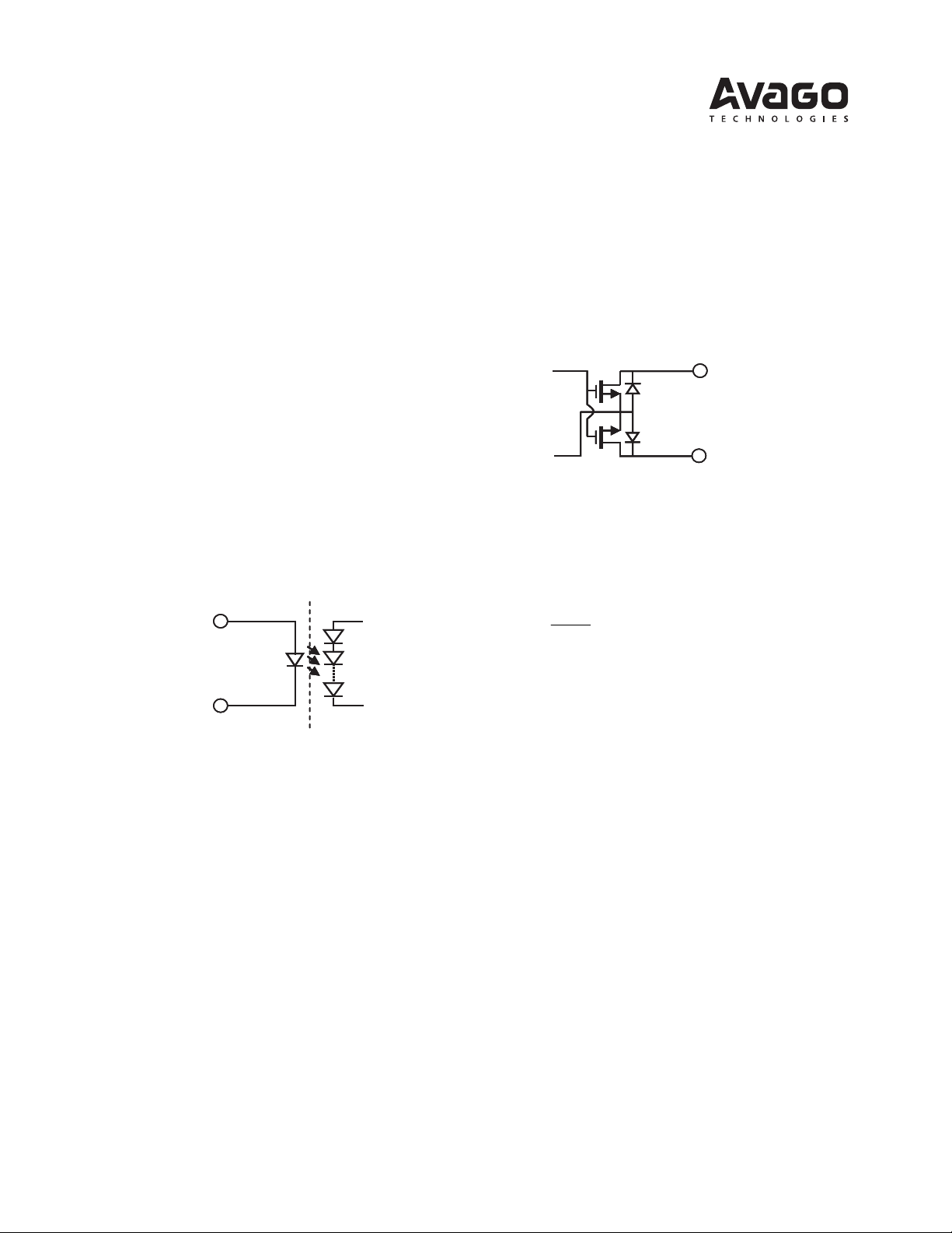
Input
The input channels of the ASSR series are LED driven,
designated as “ANODE” and “CATHODE”.
Opto-isolation
-
Anode
Output
Each output pair of the ASSR Series is made up by two
MOSFET devices with equivalent output voltage rating.
The output traces from the MOSFET drains to the screw
terminals are 50ohm lines, which can withstand 6A,
300Vac.
Drain
Drain
Figure 2. Output Stage of the ASSR Series
A load is required at the output port, which limits the
current through the two MOSFET devices. For resistive
load, its resistance should meet
V
D
R −≥
Load
Where,
I
R
max0
on
Cathode
Figure 1. Input Stage of the ASSR Series
They are commonly driven by TTL or buffered CMOS
logic gates. A current limiting resistor at each anode is
usually required to limit the current through the LED
to a proper value. The recommended input forward
current is between 3mA and 20 mA. Thus, if driven by
a 5V power supply, it is recommended to use a resistor
value of 680 ohm. It provides a forward current
between 5mA to 6.5mA where the temperature
variation between -40 0C to 85 0C and a 10% tolerance
of the resistor are taken into consideration.
R
is the resistance of the resistive load,
Load
Ron is the turn on resistance of the SSR, where R
6ohm can be used.
V
is the voltage applied on the MOSFET drain, and
D
I
is the recommended maximum output current.
o max
on
=
Page 2
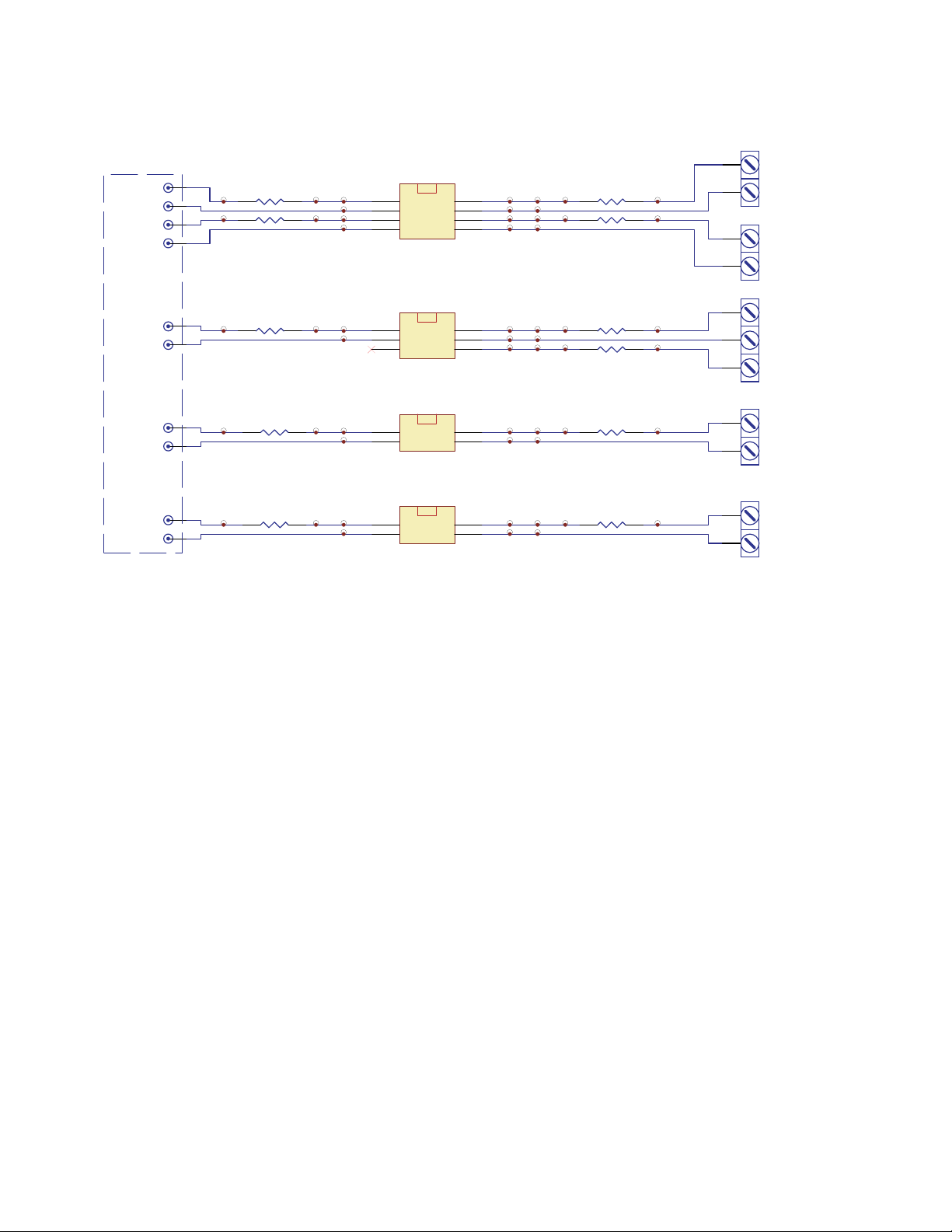
Schematic Diagram
INPUT PIN
J1
ANODE-A
J2
CATHODE-A
J3
ANODE-B
J4
CATHODE-B
J5
ANODE-C
J6
CATHODE-C
J7
ANODE-D
J8
CATHODE-D
TP8
TP7
INPUT
R1
R2
R5
R8
OUTPUT
U1
TP5
TP6
TP23TP24
TP37TP38
TP1
TP2
TP3
TP4
TP21
TP22
TP35
TP36
1
1
2
2
3
3
4
4
DIP 8PIN
Gull Wing SMT
U2
1
1
2
2
3
3
DIP 6PIN
Gull Wing SMT
U3
1
1
2
2
SOP 4PIN
TP9
8
8
TP10
7
7
TP11
6
6
TP12
5
5
TP25
6
6
TP26
5
5
4
TP27
4
4
TP39
4
TP40
3
3
TP13
TP14
TP15
TP16
TP28
TP29
TP30
TP41
TP42
TP17
TP18
TP31
TP32
TP43
R4
R3
R7
R6
R9
TP19
TP20
TP33
TP34
TP44
1
2
1
2
1
2
3
1
2
A
SCREW-2PIN
B
SCREW-2PIN
C
SCREW-3PIN
D
SCREW-2PIN
J9
ANODE-E
J10
CATHODE-E
R10
TP47TP48
TP45
TP46
1
2
U4
1
2
SSOP 4PIN
TP49
4
4
3
TP50
3
TP51
TP52
TP53
R11
TP54
The output lines to the screw terminals are50ohms lines, which can withstand 6A, 300Vac.
E
1
2
SCREW-2PIN
2
Page 3

Unpopulated Board
The evaluation PCB is 3" x 3". There are 4 mounting holes at each corner.
3
Page 4

Functional Diagram
Channel Description Functional Diagram Remarks
AU1, Gullwing
Surface Mount 8-Pin,
ASSR-xx2x-002E
BU1, Gullwing
Surface Mount 8-Pin,
ASSR-xx2x-002E
CU2, Gullwing
Surface Mount 6-Pin,
ASSR-xx1x-001E
Opto-isolation
Opto-isolation
8
1
1
2
2
3
3
4
4
Circuit
Circuit
Circuit
Circuit
Circuit
Turn-off
Turn-off
Turn-off
Turn-off
Turn-off
8
7
7
6
6
5
5
Opto-isolation
1
2
Circuit
Turn-off
6
5
DU3,
Small Outline 4-Pin,
ASSR-xx1x-003 E
E U4, Shrink Small
Outline 4-Pin,
ASSR-xx1x-006E
3
1
1
2
2
1
1
2
2
Opto-isolation
Opto-isolation
Opto-isolation
Opto-isolation
Circuit
Circuit
Circuit
Circuit
4
4
Turn-off
Turn-off
Turn-off
Turn-off
4
3
3
4
4
3
3
Note: The functional diagrams are not drawn to scale.
4
Page 5
Pinout Table
Output
Channel Description Input Current
A U1, Gullwing Surface Mount
8-Pin, ASSR-xx2x-002E
B U1, Gullwing Surface Mount
8-Pin, ASSR-xx2x-002E
C U2, Gullwing Surface Mount
6-Pin, ASSR-xx1x-001E
5mA nominal,
20mA max.
5mA nominal,
20mA max.
5mA nominal,
20mA max.
5mA nominal,
20mA max.
5mA nominal,
20mA max.
D U3, Small Outline 4-Pin,
ASSR-xx1x-003E
E U4, Shrink Small Outline
4-Pin, ASSR-xx1x-006E
5mA nominal,
20mA max.
5mA nominal,
20mA max.
Operation
In the schematic diagram, R1, R2 ,R5, R8 and R10 are
the current limiting resistors before the input pins. If
the LED is driven by a 5V power supply, a 680 ohm
resistor can be used. In the schematic diagram, R3 ,R4 ,
R6, R7, R9 and R11 are the load. The impedance of the
load should be sufficient enough to limit the output
current to less than the recommended maximum
output current.
When the LED is on (or power is applied to the LED),
the SSR (MOSFET) turns on, current will flow through
the load. When the LED is off (or there is no power
applied to the LED), the SSR (MOSFET) turns off, there
is no current flowing through the load.
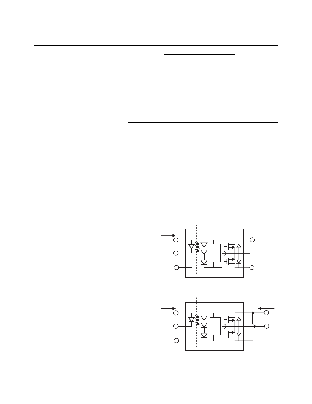
For the operation of U2, the ASSR-xx1x-001E Series is
packaged in a 6-Pin DIP with Gull Wing Surface Mount,
but only five pins are used. Pins 1 and 2 are the anode
and the cathode of the input LED, respectively, and
Pin 3 is not connected (N.C.) internally. Pins 4, 5, and 6,
at the output side can be configured as either
Connection A or Connection B as shown in figure 3.
With Connection A as shown in figure 3a, the signal at
the output of the SSR can have either positive or
negative polarity. This means that the ASSR Series can
pass either ac or dc signals. With Connection B, the
signal at the output of the ASSR must have its polarity
as indicated in figure 3b. In this configuration, pins 4
and 6 are tied together, and the ASSR can control dc
signals only. The advantage of using Connection B is
that it places two output MOSFETs in parallel with each
other, rather than in series. This configuration reduces
Load Conditions123
AC or DC
Power
AC or DC
Power
AC or DC
Power
AC or DC
N.A. Refer to product
load
AC or DC
N.A. Refer to product
load
N.C. AC or
DC load
datasheet
datasheet
Refer to product
datasheet
DC Power DC load N.C. Refer to product
datasheet
DC Power DC load DC
Power
AC or DC
Power
AC or DC
Power
AC or DC
load
AC or DC
load
N.A. Refer to product
N.A. Refer to product
Refer to product
datasheet
datasheet
datasheet
the output on-resistance of the ASSR significantly and
increases its output current capability by a factor of
two. Figure 3 also defines the polarity for the input
side of the ASSR.
Opto-isolation
I
F
1
+
V
F
2
-
N.C.
Figure 3a - Connection A (AC or DC)
N.C.
Figure 3b - Connection B (DC only)
3
Opto-isolation
I
F
1
+
+
V
F
2
-
-
3
Turn-off
Circuit
Turn-off
Circuit
6
5
4
I
O
6
5
4
+
V
O
-
-
5
Page 6

For product information and a complete list of distributors, please go to our web site: www.avagotech.com
Avago, Avago Technologies, and the A logo are trademarks of Avago Technologies, Limited in the United States and other countries.
Data subject to change. Copyright © 2006 Avago Technologies Pte. All rights reserved. Obsoletes AV01-0122EN
AV01-0309EN - July 5, 2006
 Loading...