

Page 1
ACPL-P349, ACPL-W349
Isolated IGBT or SiC/GaN MOSFET Gate Driver Evaluation Board
User Manual
Quick-Start
This manual outlines the features of the ACPL-P349/W349 Evaluation Board and the conguration required for evaluating Isolated IGBT or SiC/GaN MOSFET Gate Drivers. Visual inspection is required to ensure that the evaluation board is
received in good condition.
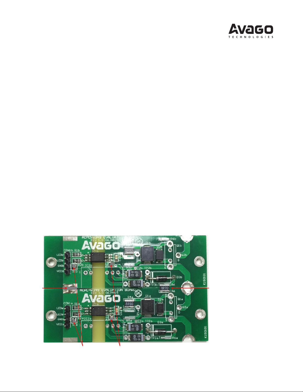
Default connections of the evaluation board are described below (refer to Figure 1):
1. Q1 and Q2 are not mounted. Either an IGBT or SiC/GaN MOSFET can be mounted at either Q1 (for TO-220 package)
or Q2 (for TO-247 package) or connected to the driver board through short wire connections from the holes provided
at Q1 or Q2;
2. D4 and R7 are not mounted (on solder side). A 15V zener footprint at D4 is provided to allow for a single DC power
supply of 15V~30V to be applied across Vcc2 and Vee if needed. A virtual ground Ve (at source pin of Q1 or Q2) can
then be generated and it acts as the reference point at the source pin of each SiC/GaN MOSFET (or emitter pin of each
IGBT). Vcc2 will then stay at 15V above the virtual ground Ve. R7 is needed to generate the bias current across D4;
3. S2 & S3 jumpers are shorted by default to connect Ve to Vee, assuming that a negative supply is not needed.
Note: If negative supply is needed, S2 & S3 jumpers need to be removed;
4. Bootstrap Diode D3b and Resistor R6 are connected by default. These 2 components are provided to help generate
Vcc2b supply through bootstrapping assuming that Vcc2a supply is available.
Note: Bootstrapping supply works only when Q1 or Q2 are mounted in a half bridge conguration and turned on and o
through proper PWM driving signals;
5. S1 is shorted by default to ground the IN- (or LED-, the cathode of LED) pin when Vcc1 is supplied. This short can be
removed if IN- cannot be grounded;
6. Upper and lower arms of the inverter will have common Vcc1 (& Gnd1), a provision is made to allow Vcc1 to be
connected by solder between upper and lower inverter PCB portions (and Gnd1 on the solder side);
7. Provisions are also made to allow Vcc2 (& Vee) to be generated from Vcc1 through a DC/DC converter at IC2. When
this DC/DC converter is used, S2, S3 (& R6) should be disconnected;
Vcc1b
Vcc1a
Vcc1a & Vcc1b(shorted)
Gnda & Gndb on solder side(also shorted)
S1(shorted) S2(shorted) S3 on solder side(also shorted)
Figure 1. ACPL-P349/W349 Evaluation board showing default connections
Note: All part references are designated with sux ‘a’ and ‘b’ to indicate lower and upper inverter arms respectively. If part references are made without
suxes, then they are valid for both upper and lower inverter arms (except R6, which is shared).
R6 mounted(soldered)
Page 2
Once inspection is performed, the evaluation board can be used to test either one of the top and bottom half bridge
inverter arms in simulation mode without the need for a IGBT or SiC/GaN MOSFET. To perform testing simply follow the
ve steps as outlined below (See Figure 2).
Testing both Arms of The Half Bridge Inverter Driver (without IGBT or SiC/GaN MOSFET)
1. Solder a 10nF capacitor across Gate and Emitter/Collector terminals of Q1 or Q2 (to simulate actual gate capacitance
of IGBT or SiC/GaN MOSFET)
2. Connect a +5V DC supply (DC supply 1) across +5V and GND terminals of CON1
3. Connect another DC supply (DC supply 2 with voltage range from 15V~30V) across Vcc2 (pin-7 of IC2) and Vee (pin-5
of IC2) terminals of IC2a respectively. This can be non-isolated for testing purposes
4. Connect drive signals;
a) A 10kHz 5V DC pulse (at slightly <50% duty) from a dual output signal generator across IN1+ & IN1- pins of CON1a
to simulate microcontroller output to drive lower arm of the half bridge Inverter
b) Another 10kHz 5V DC pulse (at 180° out of phase to 4a) from the dual output signal generator across IN2+ & IN2-
pins of CON1b to simulate microcontroller output to drive upper arm of the half bridge Inverter
5. Use a multi-channel digital oscilloscope to capture the waveforms at the following points;
a. LED signal at IN1+ pin with reference to GND
b. LED signal at IN2+ pin with reference to GND
Note: Vcc2b supply of voltage close to Vcc2a should then be successfully generated through the built-in bootstrap components D3b and R6.
c. Vga representing the output voltage of ACPL-P349/W349 (IC1a) at Gate pin of Q1a (or Q2a) with reference to Vea
d. Vgb (through an isolated probe) representing the output voltage of ACPL-P349/W349 (IC1b) at Gate pin of Q1b (or
Q2b) with reference to Veb
In2 -
In2+
4b
5b
Signal Input
-
In1
In1+
4a
5a
Signal Input
DC Supply1
2
+5V
Gnd
Figure 2. Simulation Test Setup of Evaluation Board
+-
Vcc2b
3
15~30V
DC Supply2
5d
10nF
1
Veb
5c
10nF
1
Vea
+-
2
Page 3
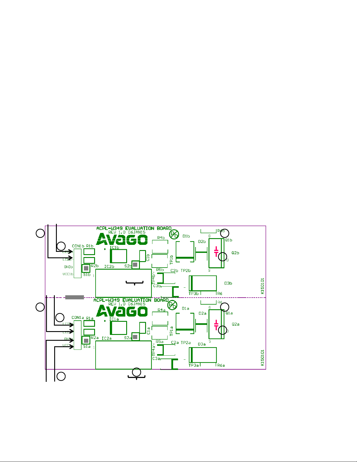
Schematics
Evaluation Board Schematics are shown in Figure 3.
LEDb +
LEDb -
Vcc1b
Gndb
LEDa +
LEDa -
Vcc1a
Gnda
CON1b
CON1a
S1b
S1a
R1b
220R
R2b
150R
R1a
220R
R2a
150R
NM
R3b
NM
R3a
IC1b
1
3
1
2
1
3
1
2
ACPL-W349
IC2b
NM
IC1a
ACPL-W349
IC2a
R05P15D/R8
6
0.1µF
5
4
7
6
5
6
0.1µF
5
4
7
6
5
C1b
VEEb
TP2b
TP3b
TP4b
C1a
VEEa
TP2a
TP3a
TP4a
Vcc2b
Vcc2a
TP1a
TP1b
R5b
NM
Vcc2b
C2b
10µF Ta
C3b
10µF Ta
R5a
NM
Vcc2a
C2a
10µF Ta
C3a
10µF Ta
VEEb
VEEa
R4b
4R7 1W
R4a
4R7 1W
S3a
S3b
R7b
NM
SS32
D1b
S2b
BYM26F
R7a
NM
SS32
D1a
S2a
BYM26F
D3b
D3a
D4b
NM
D2b
SMBJ11CA
D4a
NM
D2a
SMBJ11CA
G
R6
4R7 1W
G
D
S
VEb
D
S
VEa
NM
TO220/TO247
Q1b/Q2b
NM
TO220/TO247
Q1a/Q2a
Figure 3. ACPL-P349/W349 Evaluation Board Schematics
3
Page 4

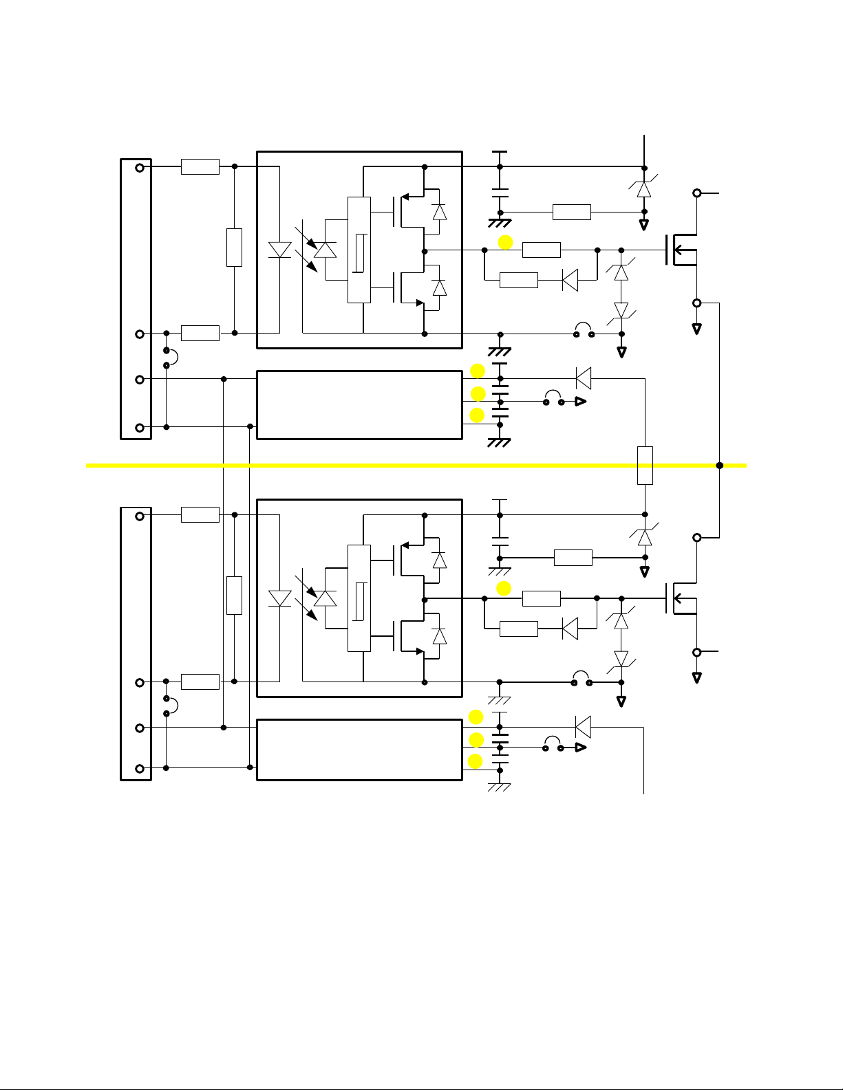
Practical Connections of the Evaluation Board Using IGBT or SiC/GaN MOSFET for Actual Inverter Test
1. Solder a IGBT or SiC/GaN MOSFET at Q1(or Q2) for top and bottom arms of the half bridge inverter isolated drivers
2. Connect a +5V DC isolated supply1 across +5V and GND terminals of CON1 for both arms of the isolated drivers;
3. Connect another isolated DC supply2 (voltage range from 15V~30V) across Vcc2a and Veea at pin-7 and pin-5 of IC2a
respectively for bottom arm
4. Connect the signal output (meant to drive the bottom arm of half-bridge inverter) from microcontroller to signal
input 1 across pin IN1+ and IN1- of CON1a of bottom inverter arm isolated driver
5. Connect the signal output (meant to drive the top arm of half-bridge Inverter) from microcontroller to signal
input 2 across pin IN2+ and IN2- of CON1b of top inverter arm isolated driver;
Note: Signal input 2 should be 180° out of phase with reference to signal input 1; Check that Vcc2b (voltage close to Vcc2a)
is generated through the bootstrap components D3b and R6
6. Use a multi-channel digital oscilloscope to capture the waveforms at the following points –
a. LED signal at IN1+ pin with reference to GND for bottom arm
b. LED signal at IN2+ pin with reference to GND for top arm
c. Vga for the gate driving voltage of Q1a(or Q2a) with reference to Vea of bottom inverter arm (dierential probe
needed)
d. Vgb for the gate driving voltage of Q1b(or Q2b) with reference to Veb of top inverter arm (dierential probe
needed)
7. Connect a power cable from output pin (marked Load) to the inverter load
8. Connect the high voltage cables from top arm SiC/GaN MOSFET drain pin (or IGBT's Collector pin) to HVDC+ and from
bottom arm SiC/GaN MOSFET source pin (or IGBT's Emitter pin) to HVDC- respectively as shown.
Note: It is advised to enable the current limiting function of the HV Power Source supplying the High Voltage DC Bus voltage
during this test to protect the Inverter and its driver circuitries.
W349
06JAN15
5
6b
IN2+
Signal Input 2
IN2 -
5
W349
15~30V
06JAN15
Microcontroller
6a
IN1+
Signal Input 1
IN1 -
4
DC Supply1
2
15~30V
+5V
Gnd
Figure 4. Connection of Evaluation Board in Actual Applications
DC Supply2
8
HVDC+
6d
1
PowerMos
Mounted
+-
K150101
7
Load
6c
1
PowerMos
Mounted
3
+-
HVDC -
8
4
Page 5

Application Circuit Description
The ACPL-P349/ACPL-W349 is an isolated Gate Driver which provides 2.5 A output current. The voltage and high peak
output current supplied by this optocoupler make it ideally suited for direct driving of IGBT or SiC/GaN Mosfet with ratings up to 1000V/100W. It is also designed to drive dierent sizes of buer stage that will make the class of IGBT or SiC/
GaN MOSFET scalable. ACPL-P349 (& ACPL-W349) provides a single isolation solution suitable for both low and high
power ratings of motor control and inverter applications.
Each of the ACPL-P349/ACPL-W349 evaluation boards, as shown in Figure 5, accommodates 2 ACPL-P349/ACPL-W349
IC’s. Therefore, each board is capable of driving top and bottom arms of the half-bridge Inverter. It allows the designer
to test the performance of the gate driver in an actual application under real-life operating conditions. Operation of the
evaluation board requires a common 5V DC isolated Supply1 on the input side and an isolated DC supply2 (range from
15V ~ 30V) for the bottom arm of Inverter IGBT or SiC/GaN MOSFET, while the DC supply needed for the top arm is easily
generated through bootstrapping included in the evaluation board.
Figure 5. Top & Bottom Views of ACPL-P349/W349 Evaluation Board
Note: As can be seen on the board, the isolation circuitry (at the far left) is contained within a small area while maintaining adequate spacing for good
voltage isolation and easy assembly.
5
Page 6

Power Supply Schemes
The Evaluation board is designed with DC supply exibility in mind and a total of 7 dierent power supply schemes are
possible (See Table 1).
Table 1. Power Supply Schemes
Scheme Vcc1 Vcc2a Veea S2a S3a D4a/ R7a Vcc2b Veeb S2b S3b D4b/ R7b Remarks
1 +5V
External
2 +5V
External
3 +5V
External
4 +5V
External
5 +5V
External
6 +5V
External
7 +5V
External
Since TVS D2 voltage is selected at a breakdown voltage of 18V, both Vcc2 and Vee voltage are not advisable to set at voltage beyond ±15V.
To use a voltage higher than 15V, please replace D2 will a bigger clamping voltage.)
+15V~30V
External
+15V~30V
External
+15V~30V
External
(15V |-0V~ -15V)
DC/DC
(=Vcc1/+15V)
DC/DC
(=Vcc1/+15V)
DC/±DC
(=Vcc1/±15V)
(+15V |-15V)
DC/±DC
(=Vcc1/±9V)
(+15V |-3V)
0V s/c s/c NM Bootstrapped*
from Vcc2a
(+15V~30V)
0V s/c s/c NM +15V~30V
External
open open 15V/1k +15V~30V External
(15V |-0V~ -15V)
0V s/c s/c NM Bootstrapped*
from Vcc2a
(+15V)
0V s/c s/c NM DC/DC
(=Vcc1/+15V)
open s/c NM DC/±DC
(=Vcc1/±15V)
(+15V |-15V)
open open 15V/1k DC/±DC
(=Vcc1/±9V)
(+15V |-3V)
0V s/c s/c NM Default (simplest)
- 2 external supplies needed
for Vcc1 & Vcc2a
0V s/c s/c NM Higher Power
- 3 external supplies needed
for Vcc1, Vcc2a & Vcc2b
open open 15V/1k Vee available
- 2 external supplies needed
for Vcc1, Vcc2a & Vcc2b
- Virtual gnds Vea & Veb
generated thru D4 &R7
0V s/c s/c NM Cheap
- Only 1 external supply is
needed (Vcc1)
- 1 Single o/p DC/DC converter for Vcc2a
0V s/c s/c NM Higher Power
- Only 1 external supply is
needed (Vcc1)
- 2 Single o/p DC/DC converters for Vcc2a & Vcc2b
open s/c NM Vee available
- Only 1 external supply is
needed (Vcc1)
- 2Dual o/p DC/DC converters
for Vcc2a,Vcc2b,Veea & Veeb
open open 15V/1k Vee available
- Only 1 external supply is
needed (Vcc1)
- Dual o/p DC/DC converters
for Vcc2a & Vcc2b
- Virtual gnds Vea & Veb
generated thru D4 & R7
Descriptions of each of the 7 dierent power supply schemes are provided below. Users are encouraged to evaluate all
seven schemes to decide which one is most suitable for his/her needs:
Power scheme 1 - This simple scheme uses two power supplies. A +5V isolated DC supply is supplied externally to power
the low voltage Vcc1 circuit. Another external supply (+15V~30V for Vcc2a) is needed for the gate driver driving the IGBT
or SiC/GaN MOSFET at bottom inverter arm. Vcc2b supply is obtained from Vcc2a by bootstrapping operation. For this
to work, the bootstrap components D3b and R6 must be connected, all S2 jumpers must be shorted so that no negative supply of Vee is allowed, and the Signal input 2 should be 180° out of phase to signal input 1. All S2’s are shorted
to connect Vee to Ve so that negative supplies are not present. S3’s are shorted by default but it has no eect on actual
operation of the board. (Please contact Avago Technologies if more information on bootstrapping is required.)
Power scheme 2 - Similar to scheme 1 in terms of Vcc1 and Vcc2a supplies with the addition of a third external supply
(+15V~30V) for Vcc2b. This is necessary when IGBT or SiC/GaN MOSFETs get bigger demanding more driving power.
Suitable for use when Qg of IGBT or SiC/GaN MOSFET rises above 200nC. (Bootstrapped power supplys can only handle
low driving power.)
Power scheme 3 - This scheme uses 3 external supplies at Vcc1, Vcc2a and Vcc2b with the added advantage of negative
supplies for Vee (or Veea & Veeb) by introducing a 15V zener at D4 and R7 of around 1kOhm to provide proper biasing
current at D4. For this scheme to work, both S2 and S3 jumpers must be open while the external supplies (+15V~24V) at
high voltage driver side are to be connected across Vcc2 and Vee pins only, not Ve pin. As the external supply changes
from +15V to +24V, Vcc2 will stay at +15V, but Vee changes from -0V to -15V, all with reference to virtual ground at Ve.
6
Page 7

Power scheme 4 - This is another simple scheme oered as an alternative to scheme 1. Here, only 1 external supply is
needed (for Vcc1). Vcc2a is obtained by a lower power DC/DC converter at IC2a with Vcc1 as Vin and +15V output at
Vcc2a with reference to Vea. Vcc2b supply is obtained from Vcc2a by bootstrapping operation. For this to work, the
bootstrap components D3b and R6 must be connected, all S2 jumpers must be shorted so that no negative supply of
Vee is allowed, and the Signal input 2 should be 180° out of phase to Signal input 1. S2 is shorted to connect Vee to Ve
so that negative supply is not present. S3’s are shorted by default but it has no eect on actual operation of the board.
Power scheme 5 - Similar to scheme 4 in terms of Vcc1 and DC/DC converter for Vcc2a. A second DC/DC converter at
IC2b with Vcc1 as Vin and +15V output at Vcc2b with reference to Veb. All S2’s are shorted to connect Vee to Ve so that
negative supplies are not present. S3’s are shorted by default but it has no eect on actual operation of the board.
This is necessary when IGBT or SiC/GaN MOSFETs get bigger demanding more driving power. Suitable for use when Qg
of IGBT or SiC/GaN MOSFET rises above 200nC. (Bootstrapped power supplys can only handle low driving power.)
Power scheme 6 - Similar to scheme 5 with the use of Vcc1 and 2 DC/DC converters. However, each of the DC/DC converters should have dual outputs set at ±15V to allow for the availability of negative Vee (at Veea & Veeb). Therefore, all
S2’s must be open, while all S3’s must be shorted.
Power scheme 7 - This scheme is useful if dual-output ±15V DC/DC converters are not available or dual-output ±9V DC/
DC converters are preferred. 15V Vcc2 can still be obtained using ±9V DC/DC converters by introducing a 15V zener at
D4 and R7 of around 1kOhm to provide proper biasing current at D4. For this scheme to work, both S2 and S3 jumpers
must be open. As the total voltage across Vcc2 with reference to Vee stays at 18V(=9V+9V), Vcc2 of 15V will be obtained
through the 15V D4 zener, and -3V at Vee, all with reference to virtual ground at Ve.
Using the Board
The evaluation board is easily prepared for use with only minor work being required (soldering cables for DC supplies,
proper cables for HVDC+/HVDC- high voltage bus, and load connections). The default connections of the evaluation
board when shipped to customers are shown in the Table 1.
Output Measurement
A sample of Input LED and various output waveforms are captured and shown in Figure 6 below. Default setup connection is adopted except with Q1a and Q1b IGBT or SiC/GaN MOSFETs mounted. The IGBT or SiC/GaN MOSFETs used have
a gate capacitance equivalent to 10nF.
Figure 6 also shows that once bootstrap supply is adopted, the output voltage amplitude at the top inverter arm will be
slightly less than the voltage at the bottom inverter arm, at 180° out of phase. (IN1+ is set at 49% duty ratio, while IN2+
(not shown) is also set with 49% duty ratio plus a turn-on delay of 100ns with reference to IN1+).
IN1+
Vgs (Q1a)
Vgs (Q1b)
Figure 6. Input LED signal and IGBT or SiC/GaN MOSFET Gate Voltage Waveforms
7
Page 8
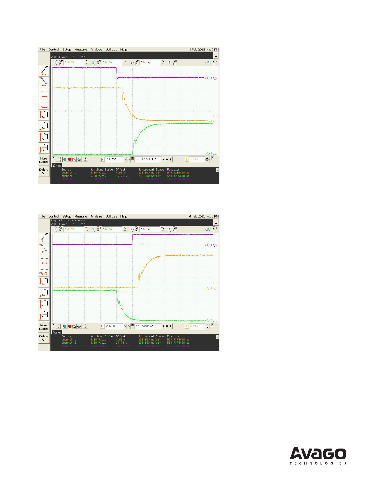
Figure 7 shows the turn-o signal of IN1+, the turn-o signal at gate of Q1a and the turn-on signal at gate of Q1b.
IN1+
Vgs (Q1a)
Vgs (Q1b)
Figure 7. Turn-o & Turn-on Gate waveforms of Q1a & Q1b
Figure 8 shows the turn-on signal of IN1+, the turn-on signal at gate of Q1a and the turn-o signal at gate of Q1b.
IN1+
Vgs (Q1a)
Vgs (Q1b)
Figure 8. Turn-on & Turn-o Gate waveforms of Q1a & Q1b
As can be seen from Figures 7 and 8, the turn-o speed of the IGBT or SiC/GaN MOSFET will be quite slow, due to the
capacitive eects of D2 and the gate capacitance of Q1. To improve the turn-o speed, the board is equipped with diode
resistor pair footprints at D1 and R5 (not mounted NM) to increase the gate current during turn-o. The turn-on and
turn-o speed can be further improved by reducing the gate resistance of R4, however, care must be taken to ensure
that the gate drive current is not more than 2.5A.
For product information and a complete list of distributors, please go to our web site: www.avagotech.com
Avago, Avago Technologies, and the A logo are trademarks of Avago Technologies in the United States and other countries.
Data subject to change. Copyright © 2005-2015 Avago Technologies. All rights reserved.
AV02-4749EN - February 9, 2015
 Loading...