

Page 1

Gate Drive Evaluation Board
for ACPL-P343/W343 4.0 Amp Gate Drive Optocoupler
with Rail-to-Rail Output Voltage in Stretched SO6
User’s Guide
Product Description
The ACPL-P343/W343 is a 4.0 A peak output current gate
drive optocoupler with rail-to-rail output voltage and very
short propagation delay that help to improve the e ciency and reliability of IGBT gate driving.
ACPL-P343/W343 is ideally suited for driving IGBTs and
power MOSFETs used in motor control and renewable
energy inverter applications. The voltage and current
supplied by these optocouplers make them suitable for
direct driving of IGBTs with ratings up to 1200 V and 200 A.
ACPL-W343 has an insulation voltage of V
V
. It is also immune to common-mode voltage tran-
PEAK
sients as high as 1.5 kV and as fast as 35 kV/s.
IORM
= 1140
About Evaluation Board
The ACPL-P34X/W34X evaluation board allows a powerinverter designer to easily test the drive, rail-to-rail and
speed capability of the ACPL-P343/W343 gate drive optocoupler. The evaluation board includes two separate gate
drive channels (one optocoupler per channel) making it
a half-bridge topology for driving directly the gates of
high-side and low-side IGBTs of a power inverter (such
as single-phase motor inverter or one phase of a 3-phase
motor inverter). This evaluation board can also support
ACPL-P341/W341 and ACPL-P340/W340.
Features
Half-Bridge topology
Footprints for bootstrap power supply con guration
Works for IGBT TO-220 / TO-247 type
Able to evaluate the 4 A drive, rail-to-rail and speed
performance
Footprints for PCB mounting terminal blocks for wire
connections to motor
Split resistors network to achieve high CMR response
Example of good bypass capacitors layout
Supports ACPL-P341/W341 and ACPL-P340/W340
Applications
Isolated IGBT/MOSFET Gate Drive
AC and Brushless DC Motor Drives
Industrial Inverters
Renewable Energy Inverters
Uninterruptible Power Supplies (UPS)
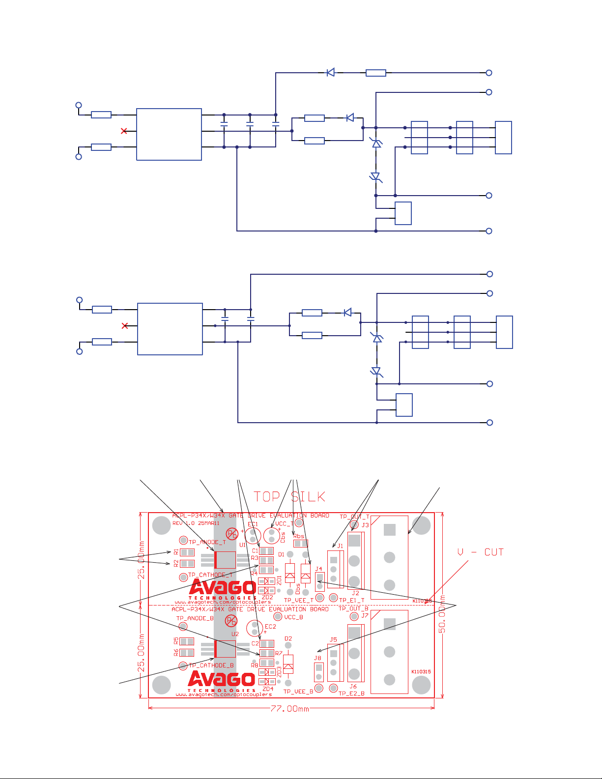
Diagrams
The schematic diagram of the evaluation board can be
found in Figure 1 and 2. The top view of evaluation board
is in Figure 3.
CAUTION: When operating the board connected to a half-bridge dual IGBT (with the dual IGBT con-
nected to high-voltage rails) never short the output ground planes and scope ground together!! Also
when probing points on the upper gate-drive channel use a scope with adequate voltage rating!
Page 2
TP_ANODE_T
1
1
TP_CATHODE_T
205 ohm
R1
137 ohm
R2
12
1
2
12
3
Anode
NC
Cathode
ACPL-P34X/W34X
U1
Vcc
Vout
Vee
1
6
C1
1 MF
50 V
5
2
4
1
1
EC1
Cbs
NM
2
NM
2
Figure 1. Schematic Diagram for ACPL-P34X/W34X Evaluation Board – Top
TP_ANODE_B
1
1
TP_CATHODE_B
205 ohm
R5
137 ohm
R6
12
1
2
12
3
Anode
NC
Cathode
ACPP-P34X/W34X
U2
Vcc
Vout
Vee
6
1
1
1 MF
50 V
EC2
NM
2
C2
5
2
4
Figure 2. Schematic Diagram for ACPL-P34X/W34X Evaluation Board – Bottom
1 2
R3
1 2
NM
R4
1 2
NM
R7
1 2
NM
R8
1 2
NM
Dbs
NM
D1
1 2
SS32
D2
1 2
SS32
Rbs
1 2
NM
1
ZD1
2
ZD2
1 2
12
ZD3
ZD4
1 2
3P_TO220
1
2
3
2P_HEADER
1
2
J4
1
2
3
2P_HEADER
1
2
J8
J1
NM
3P_TO220
J5
NM
G1
C1
E1
G2
C2
E2
3P_TO247
1
2
3
3P_TO247
1
2
3
NM
1
VCC_T
1
TP_OUT_T
3P_HEADER
1
1
1
1
1
1
J3
1
2
3
NM
TP_E1_T
TP_VEE_T
VCC_B
TP_OUT_B
3P_HEADER
J7
1
2
3
NM
TP_E2_B
TP_VEE_B
TP_G1
TP_C1
TP_E1
TP_G2
TP_C2
TP_E2
J2
NM
J6
ACPL-P343/W343
Top Gate Driver
Split Resistors
Input LED Drive
Gate Resistors
R3, R4, R7 & R8
ACPL-P343/W343
Bottom Gate Driver
Figure 3. Top Layer View
2
Isolation
Barrier
Bypass Cap
C1 & C2
Bootstrap Capacitor,
Resistor and Diode
IGBT TO-220/247
Type Package
PCB Mounting
Terminal Blocks
J3 & J7
Negative Power Supply
Jumpers J4 & J8
Page 3

Test Connection and Operation
The denotations or symbols used below refer to High Side,
the top gate driver (U1) operation. If operating in a halfbridge topology, please refer to the bottom gate driver’s
(U2) denotations or symbols in schematic diagram, Figure 2.
ACPL-P343/W343 Input Side:
1. LED input current: ACPL-P343/W343 has a LED input
gate control. Split resistors network in the ratio of 1.5:1
are used to achieve high CMR response. At this ratio,
R1 will be 205 and R2 will be 137 . Connecting “TP_
ANODE_T” and “TP_CATHODE_T” to a 5 V input pulse
signal will drive a recommended LED current of about
10 mA.
ACPL-P343/W343 Output Side
1. Output positive power supply: Connect the +15 V of an
isolated DC power supply to “VCC_T” and the common
to “TP_E1_T” test points. “TP_E1_T” is connected to the
IGBT emitter.
2. Output negative power supply (optional): If only single
positive output power supply is required, short the
open connection J4. For negative output power supply,
connect the -15 V of the isolated DC power supply to
“TP_VEE_T” and the common to “TP_E1_T” test points.
Remove any short circuit connection on J4 and replace
J4 with appropriate bypass capacitors.
3. Output positive bootstrap power supply (optional for Top,
High side only): For single positive output power supply,
short the open connection J4. Connect the +15 V
power supply of the Bottom side, “VCC_B” to the Top
side “VCC_T”. To complete the bootstrap power supply,
solder appropriate bootstrap resistor “Rbs”, diode “Dbs”
and Capacitor “Cbs”.
4. Gate resistors: Solder appropriate R3 for IGBT gate
discharging and R4 for IGBT gate charging.
5. Output: Monitor the output or the gate of IGBT by
connecting an oscilloscope between “TP_OUT_T” to
“TP_E1_T”.
For product information and a complete list of distributors, please go to our web site: www.avagotech.com
Avago, Avago Technologies, and the A logo are trademarks of Avago Technologies in the United States and other countries.
Data subject to change. Copyright © 2005-2011 Avago Technologies. All rights reserved.
AV02-2927EN - April 20, 2011
 Loading...