

Page 1
EVBD-ACPL-C87B/C87A/C870
Isolated Voltage Sensor Evaluation Board
User Guide
Board Description
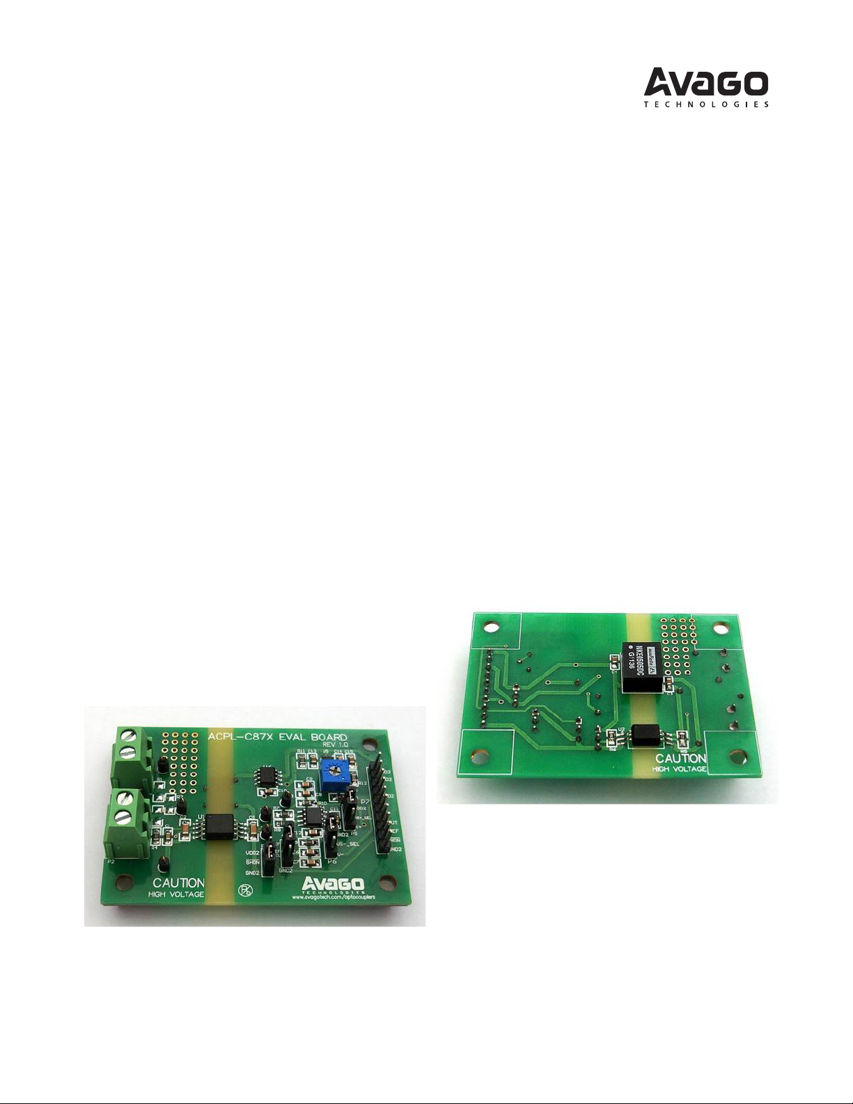
The ACPL-C87x evaluation board (see Figure 1 and Figure 2) is designed to support the evaluation of the ACPL-C87x precision optically isolated voltage sensors. The
ACPL-C87x series is available in three choices: ACPL-C87B
(±0.5% gain tolerance), ACPL-C79A (±1% gain tolerance)
and ACPL-C790 (±3% gain tolerance). Featuring 2 V
put range and 1 GΩ high input impedance, these isolation
ampliers are specically designed for voltage sensing in
electronic power converters applications, including motor
drives and renewable energy systems. The ACPL-C87x is
identied as U1 on the evaluation board.
On the input side of the evaluation board, power terminals
P1 and P2 are provided for incoming voltage connection.
This voltage is required to scale down to suit the input
range of the voltage senor. This can be achieved by choosing appropriate resistors and mount on the footprints provided for R1 through R3. On the output side of the evaluation board, header connector P7 provides a connection
port for power supply to the board and signal interface
with next stage such as an analog to digital converter or a
signal processing and control device.
Note:
1. The ACPL-C87x data sheet species 2 V as the nominal input range.
Full scale input range (FSR) is 2.46 V.
[1]
in-
Features
• User-congurable voltage sensing range up to 1230 V
• Single 5 V supply or dual supply up to ±15 V
• Onboard oset calibration
• Onboard isolated 5 V power supply for high voltage
side
• User-controllable shutdown
Voltage Sensor Applications
• Isolated voltage sensing in AC and servo motor drives
• Isolated DC-bus voltage sensing in solar inverters, wind
turbine inverters
• Isolated sensor interfaces
• Signal Isolation in data acquisition systems
• General purpose voltage isolation
Figure 1. The ACPL-C87x evaluation board (top view)
Figure 2. The ACPL-C87x evaluation board (bottom view)
Page 2
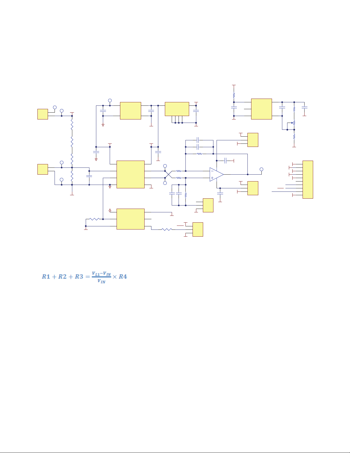
Schematic
Figure 3 shows the evaluation board schematic. In a typical voltage sensing implementation, a resistive voltage divider
is used to scale the DC-link voltage to suit the input range of the voltage sensor. Power terminals P1 and P2 are used to
connect to the DC-link voltage across nodes L1 and L2 to be monitored. This voltage, denoted as VL1 as L2 is connected
to the reference point GND1, is scaled down through a resistive divider consists of resistors R1 through R4 in series. On
this board, R4 has a xed value of 10 kΩ, although it can be replaced by another value, if desired.
VDD2
GND1
C1
22 nF
GND1
C2
100 nF
TP5
C3
0.47 µF
VDD1
GND1
GND1
0.47
µF
C4
GND2
1
C5
100 nF
TP7
TP6
R6
700
U6
OUT
GND
7
6
LM78L05ACM
10K, 1%
R7
R8
10K, 1%
C6
1 nF
GND2
3
SHDN
2
C7
1 nF
VDD2
GND2
V+
8
IN
C10
100 nF
GND2
1 nFC8
1 nFC9
R10
10K, 1%
R9
10K, 1%
V
ref
REF-SEL
GND2
P3
1
2
3
Jumper
default position: Pin 1-2
0.1 µFC11
2
7
6
3
4
VS-_SEL
C12
P4
1
GND2
2
3
Jumper
default position: Pin 1-2
GND2
VS+_SEL
V+
U4
OPA237UA
V-
U3
5
+V
out
7
-V
out
NKE0505DC
U1
1
V
DD1
2
V
IN
3
SHDN
4
GND1
ACPL-C87X
U2
4
GND
5
V
O
6
V
CC
ACPL-W50L
+V
in
-V
in
V
DD2
V
OUT+
V
OUT-
GND2
CATHODE
ANODE
4
1
GND2
VDD2
8
7
6
5
GND2
3
2
NC
1
P1
2
1
Power Terminal
P2
2
1
Power Terminal
Put an area of through-holes for prototyping
TP1
TP2
L1
R1
Leave blank
R2
Leave blank
R3
TP3
Leave blank
R4
TP4
10k, 1%
L2
R5
10k
VDD1
Figure 3. The ACPL-C87x evaluation board schematic
Given that the voltage sensor ACPL-C87x’s nominal input voltage for VIN is 2 V, a user needs to choose resistors R1, R2
and R3 according to Equation 1.
R11
1K
GND2
C13
1 µF
VDD2
GND2
V
= 0.4V*(1+(R12+R
ref
U5
IN4OUT
3
DNC
2
P5
1
2
3
Jumper
default position: Pin 1-2
P6
1
2
3
Jumper
default position: Pin 1-2
GND
LT6650CS5(IS5)
TP8
V
out
FB
)/R14) = 0.48 to 0.52 V
Pot
5
C14
1 nF
1
V
GND2
GND2
SHDN
GND2
V
ref
3
GND2
DD2
V+
V-
V
V
C15
R12
1 µF
20K
GND2
1
R13
R
10k
Pot
2
R14
100K
P7
1
2
3
4
5
6
out
7
ref
8
9
10
Header
- Equation 1
For example, if VL1 = 600 V, then the combined value of R1, R2 and R3 = 2990 kΩ.
Choosing resistors is exible. One method is to combine several resistors to match the target value; e.g., 2 MΩ, 430 kΩ
and 560 kΩ resistors make up 2990 kΩ exactly. In this way, VIN of 2 V corresponds to VL1 of 600 V. However, in the cases
that VL1 has a dierent value from 600 V, specic resistance values might be dicult to nd. Another method is to round
up the target value to a convenient value 3 MΩ to make choosing resistors easier; e.g., 1 MΩ is a common value and 3
pieces of it make 3 MΩ. In this way, the scaling relationship needs some ne tune. In the same example with VL1 = 600 V,
R1+R2+R3 = 3 MΩ, and R4 = 10 kΩ, VIN is solved to be 1.993 V.
After deciding resistance for R1 through R3, surface mount type devices can be mounted on the footprints provided. In
case only through-hole type resistors are available, the prototyping area can be used instead.
The down-scaled input voltage is ltered by the anti-aliasing lter formed by R4 and C1 with corner frequency of 723 Hz
[1]
and then sensed by the ACPL-C87x. A dierential output voltage that is proportional to the input voltage is created
on the other side of the optical isolation barrier.
Note: 1. The total value of R1 through R3 in series is usually much larger than R4, therefore neglected in calculation.
Following the isolation amplier, an OPA237 congured as a dierence amplier converts the dierential signal to a
single-ended output. This stage can be congured to further amplify the signal, if required, and form a low-pass lter
to limit the bandwidth. In this circuit, the dierence amplier is designed for a gain of 1 with a low-pass lter corner frequency of 8 kHz. Resistors R9 and R10 can be selected for a dierent gain. The bandwidth can be reduced by increasing
capacitance for C6 and C8.
2
Page 3

With the ACPL-C87x gain of 1 and P4 jumper position on P1-2, the overall transfer function is:
- Equation 2
or
- Equation 3
As long as the P4 jumper position remains on P1-2, then Equation 2 and 3 hold true. If the P4 jumper is changed to P2-3,
then the V
in Equation 2 and 3 will be set to 0 V. In this case, the onboard oset calibration function discussed in the
REF
subsequent section cannot be used.
Output voltage V
representing the line voltage on the high voltage side is connected to the controller through P7
OUT
pin 7.
Power Supplies
The ACPL-C87x evaluation board operates from a single 5 V or dual supply up to ±15 V. To operate the board from a
single 5 V supply:
1. Leave header jumpers P3 through P6 at their default positions as indicated in the schematic (Figure 3).
2. Connect the 5 V supply source to nodes V
same power supply for the signal processing and control device.
To operate the board from dual supply such as ±10 V:
1. Connect +10 V, COM and -10 V to nodes V+, GND2 and V- through P7 pin 3, 4 and 5, respectively.
2. Change P5 and P6 jumpers pin 2-3 position, respectively.
In the dual supply method, the V
[1]
node receives 5 V supply through a voltage regulator LM78L05 (U6) from V+
DD2
node; therefore, a recommendation for V+ node is +7 V to +15 V.
Besides supplying to the ACPL-C87x output side, it is also connected to an isolated DC-DC converter (U3) to produce a
oating 5 V supply. This oating 5 V supply, denoted as V
W50L optocoupler. The isolated DC-DC converter is included in the evaluation board for evaluation convenience. To
make this isolated voltage sensing solution cost-eective in mass production, the 5 V supply would usually be supplied
by a oating power supply, which in many applications could be the same supply that is used to drive the high-side
power transistor. A simple three-terminal voltage regulator will provide a stable voltage. Another method is to add an
additional winding to an existing transformer to produce a 5 V supply.
Note:
1. The ACPL-C87X data sheet species VDD2 of 3 V to 5.5 V.
and GND2 through P7 pin 1 and 2. In many cases, the 5 V supply is the
DD2
, is used to operate the ACPL-C87x input side and the ACPL-
DD1
Onboard Oset Calibration
A voltage reference device, the U5 LT6650 in Figure 3, is included in the circuit to provide a shifted “virtual ground” for
VOUT, thereby enables onboard oset calibration. To use this function, follow these simple steps:
1. Provide power supply to the board. Ensure the P4 jumper position is at Pin 1-2.
2. Set line voltage to the evaluation board to 0 V, or leave it unconnected.
3. Adjust the trimmer resistor R13 to set V
With these steps, V
of 0.500 V corresponds to a 0 V of VIN, therefore oset voltage due to the voltage sensor ACPL-
OUT
reading at 0.500 V.
OUT
C87x and the post-amp OPA237 is calibrated out. The controlled oset of 0.500 V then needs to be registered in the following stage signal processor and subtracted from measurement readings to obtain actual voltage sensor input.
Voltage Sensor Shutdown
The voltage sensor ACPL-C87x features a shutdown mode, which can be activated with a high level logic input on the
shutdown pin (pin 3). In this mode, the IDD1 supply current is reduced to only 15 µA, making it suitable for battery-powered devices and other power-sensitive applications. In the evaluation circuit, the optocoupler U2 ACPL-W50L sends
the shutdown logic from the low voltage controller side across the isolation barrier to the voltage sensor shutdown pin
SHDN. Controller shutdown signal through P7 pin 9 needs to be a Low logic as the ACPL-W50L produces inversed signal
from input to output. To manually turn the ACPL-C87x to shutdown mode, jumper P3 can be used: put jumper on pin
1-2 for normal operation; change to pin 2-3 to shut down.
3
Page 4
In shutdown mode, the ACPL-C87x outputs topple to saturated levels to dierentiate from normal operation mode.
Table 1 lists the voltage sensor outputs and the post-amp output when the voltage sensor is on standby.
Table 1.
ACPL-C87x OPA237
V
0 – 3 V 0.005 V 2.75 V -2.74 V 0.23 V
Note:
When the board is operated from a dual supply, the V
V
IN
OUT+
V
OUT-
V
– V
OUT+
OUT-
V
(test conditions)
OUT
-2.74 V (dual ±10 V supply, REF-SEL connected to V
(single 5 V supply)
OUT
connected to an ADC input, then some means of protection are required to protect the ADC from damage.
-2.24 V (dual ±10 V supply, REF-SEL connected to GND2)
can reach -2.74 V when the voltage sensor is shut down. If this voltage is directly
REF
);
Use the Board with Caution
To use the board for bench measurement that involves only a low voltage of several volts from an isolated voltage
source, a user can connect input to P2 directly, without the need of the resistive divider. Adjust the input voltage to an
appropriate level to carry out measurements.
To connect the board to a high voltage source such as a DC-link bus or a photovoltaic panel output, the user can connect
the high voltage nodes to P1 pin 1 and P2 pin 1, using the onboard voltage divider with appropriate resistors mounted
to R1 through R3 footprints. If through-hole resistors are used to implement the voltage divider, the prototyping area
can be used -- connect high voltage across P1 pin 2 and P2 pin 1. With high voltage presence on the board, caution of
electric shock is required when handling the board as the high voltage side is not shielded.
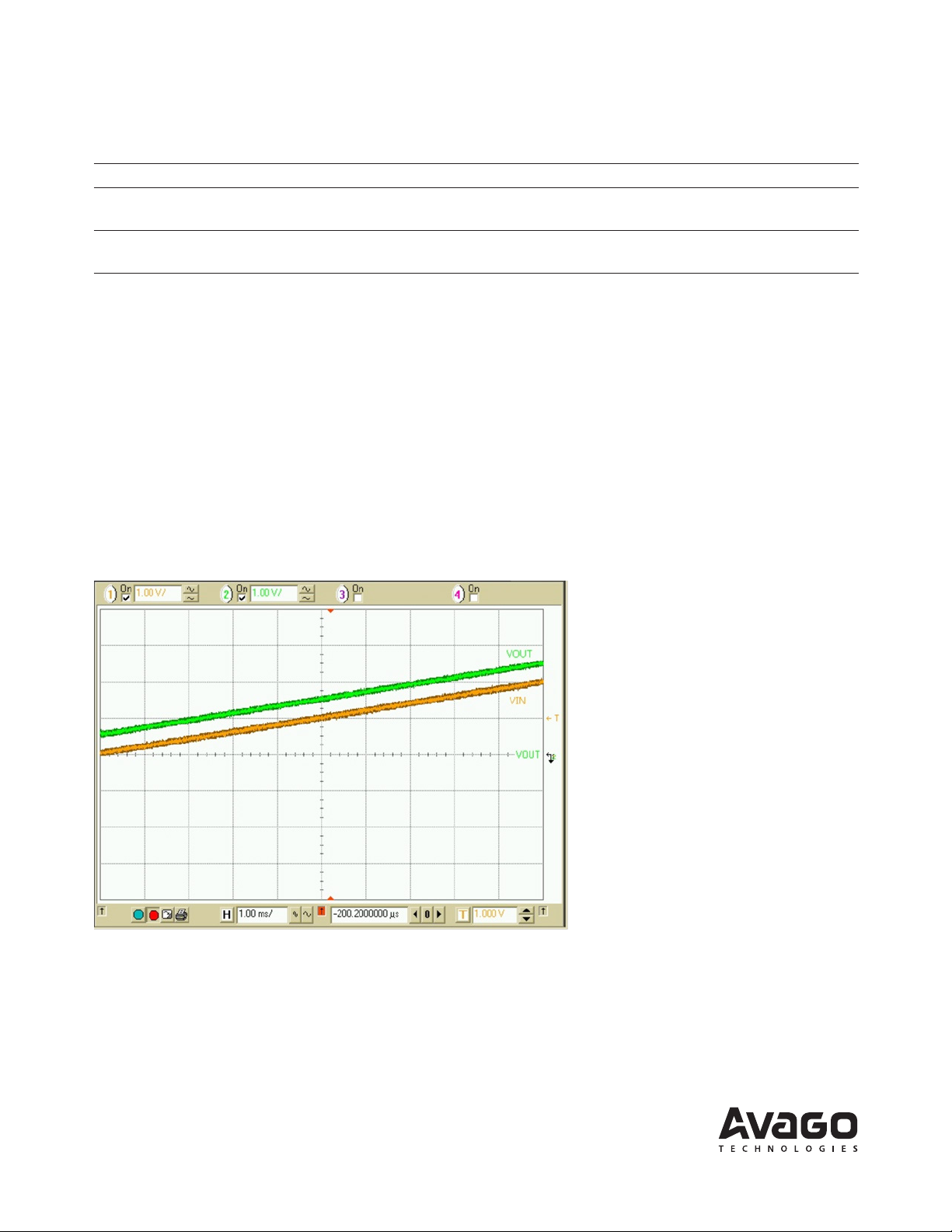
Figure 4 shows an oscilloscope screen shot of a measurement with VIN = 0 V to 2 V linear input, and V
linear output. The dierence of 0.5 V is the V
Figure 4. Scope screen shot of a measurement with 0-2 V linear input
set during calibration.
REF
= 0.5 V to 2.5 V
OUT
For product information and a complete list of distributors, please go to our web site: www.avagotech.com
Avago, Avago Technologies, and the A logo are trademarks of Avago Technologies in the United States and other countries.
Data subject to change. Copyright © 2005-2013 Avago Technologies. All rights reserved.
AV02-4293EN - September 11, 2013
 Loading...