

Page 1

EVBD-ACSL-7210 PROFIBUS / SPI Evaluation Board
5
ACSL-7210 Dual-Channel (Bidirectional) 25 MBd
CMOS Buered Input Digital Optocoupler
User Guide
Product Description
Avago’s ACSL-7210 optocoupler utilizes the latest CMOS
IC technology to achieve outstanding speed and low
power performance of minimum 25 MBd data rate.
Available in SO-8 package, the basic building blocks of
each channel in ACSL-7210 are a CMOS LED driver IC, a
high speed LED and a CMOS detector IC. A CMOS logic
input signal controls the LED driver IC, which supplies current to the LED. The detector IC incorporates an integrated
photodiode, a high speed trans-impedance amplier, and
a voltage comparator with an output driver.
Functional Diagram
8
VDD
1
1
2
VO
A
VI
3
B
4
GND
1
Shield
ACSL-7210
TRUTH TABLE (POSITIVE LOGIC)
Input side
VDD state
Power
Supplied
No Power Power
Output side
VDD state V
Power
Supplied
Supplied
VDD
2
7
VI
A
VO
6
B
GND
2
I
HIGH OFF HIGH
LOW ON LOW
X OFF HIGH
LED V
O
Features
• Dual-Channel (Opposite direction orientation)
• 3.3 V and 5 V CMOS Compatibility
• High Speed: DC to 25 MBd
• CMOS output and buer input
• Operating temperature: –40°C to +105°C
• Safety and Regulatory Approvals:
- UL 1577 – 3750 Vrms for 1 minute
- IEC/EN/DIN EN 60747-5-5
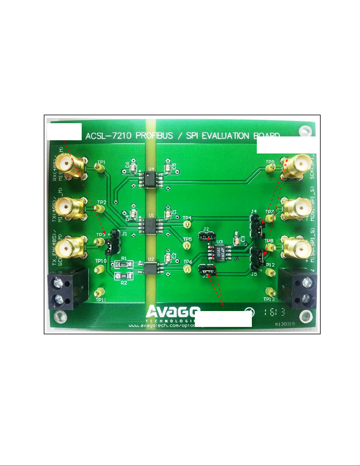
About the Evaluation Board
The ACSL-7210 PROFIBUS / SPI evaluation board is congurable for either PROFIBUS (RS-485) or SPI communication. The board will accept both 3.3V and 5V power supplies.
When congured for PROFIBUS communication, the
ACSL-7210 bi-directional optocoupler provides isolation
for both the transmitting and receiving channels. Isolation
for the Tx Enable signal is provided by the ACPL-M61L, ultra low power 10MBd CMOS digital optocoupler. A standard RS-485 transceiver (max. data rate of 20Mbps) is included on the board.
For SPI interface, the ACSL-7210 is used for serial data in/
out isolation. Isolation for the clock signal is provided by
ACPL-077L, low power 25MBd CMOS digital optocoupler.
Figures 1 and 2 shows the jumper settings for PROFIBUS
and SPI operation. Figure 3 shows the schematic diagram
of the evaluation board.
Page 2
Board Connection and Operation
PROFIBUS Operation (Refer to Figure 1)
1. Short i) lower 2 pins of J1, ii) lower 2 pins of J4, and iii) upper 2 pins of J5.
2. The jumpers on J2 and J3 should be connected.
3. Connect a 3.3/5V power supply to VDD1 and GND1.
4. Connect a 3.3/5V power supply to VDD2 and GND2.
5. Connect the RS-485 dierential lines to SMA connectors +(485) and –(485).
6. Connect SMA connectors TX_EN(485), TX(485) and Rx(485) to microcontroller.
Short lower
2 pins of J1
Short lower 2 pins of J4,
and upper 2 pins of J5
Figure 1. Conguration for PROFIBUS (RS-485) Operation
2
Jumpers on J2 and J3
should be connected.
Page 3

SPI Operation (Refer to Figure 2)
1. Short i) upper 2 pins of J1, ii) upper 2 pins of J4, and iii) lower 2 pins of J5.
2. J2 and J3 should be left open.
3. Connect a 3.3/5V power supply to VDD1 and GND1.
4. Connect a 3.3/5V power supply to VDD2 and GND2.
5. The master device should be connected to SCK(SPI_M), MOSI(SPI_M), and MISO(SPI_M).
6. The slave device should be connected to SCK(SPI_S), MOSI(SPI_S), and MISO(SPI_S).
Short upper
2 pins of J1
Short upper 2 pins of J4,
and lower 2 pins of J5
Figure 2. Conguration for SPI Operation
3
J2 and J3 should
be left open
Page 4

C6
100n
VDD1
U4
1
2
3
4
ACPL-077L
VDD1
VI
NC
GND1
VDD2
GND2
VDD2
C5
100n
8
7
NC
6
VO
5
TP9
SCK(SPI_S)
VDD1
C4
U1
100n
1
VDD1
2
VOA
3
VIB
GND14GND2
ACSL-7210
VDD1
U2
R1
1
AN
510
R2
3
CA
360
ACPL-M61L
TP10 TP12
VDD1
TP11 TP13
RX(485)/MISO(SPI_M)
TX(485)/MOSI(SPI_M)
TX_EN(485)/SCK(SPI_M)
VDD1
GND1
TP1
TP2
TP3
J1
3
2 1
1
2
Figure 3. Schematic Diagram for ACSL-7210 Evaluation Board
VDD2
VOB
VDD
GND
VIA
VDD2
C1
100n
C2
100n
TP5
TP6
TP4
1
2
J2
1 2
J3
1
VDD2
GND2
21
J4
-(485)/MOSI(SPI_S)
3
TP7
21
J5
VDD2
U3
1
RO
RE_
DE
DI
VCC
B
A
GND
2
3
4
2
RS485 Trans
C3
100n
8
7
6
5
+(485)/MISO(SPI_S)
3
TP8
8
7
6
5
VDD2
6
5
VO
4
VDD2
For product information and a complete list of distributors, please go to our web site: www.avagotech.com
Avago, Avago Technologies, and the A logo are trademarks of Avago Technologies in the United States and other countries.
Data subject to change. Copyright © 2005-2013 Avago Technologies. All rights reserved.
AV02-4309EN - September 30, 2013
 Loading...