

Page 1
ACPL-M61L/064L SPI Evaluation Board
ACPL-064L
ACPL-M61L
Ultra Low Power 10MBd Digital CMOS Optocouplers
User’s Guide
Product Description
The ACPL-M61L (single-channel in SO-5 footprint) and
ACPL-064L (dual-channel in SO-8 footprint) are low power,
low input current, 10 MBd digital optocouplers. They are
designed to operate at VDD from 2.7 V to 5.5 V and I
DD
of
1.3 mA/ch max. The input LED can be driven with a low
input driving current of 1.6 mA.
The ACPL-M61/064L has a common mode transient
immunity of 20 kV/µs (min.) at VCM = 1000 V.
Applications
• Communication Interface: RS485, CANBus, I2C
• Microprocessor System Interfaces
• Digital isolation for A/D, D/A converstion
Functional Diagram
8
V
DD
7
Vo1
6
Vo2
5
GND
Anode
Cathode
6
V
DD
1
3
Cathode 1
5
Vo
Cathode 2
4
GND
Anode 1
Anode 2
1
2
3
4
SHIELD
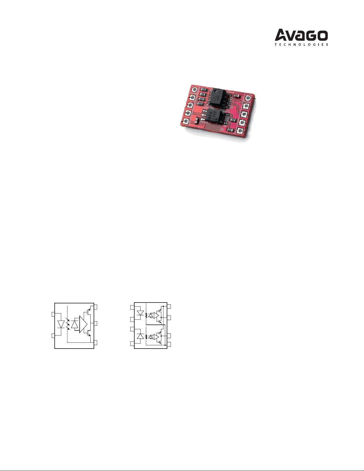
About Evaluation Board
The ACPL-M61L/064L evaluation board allows designers
to evaluate Avago digital optocouplers easily on a solderless breadboard.
The evaluation board contains one ACPL-064L and one
ACPL-M61L (orientated 180°) to provide a total of three
channels (two in the forward direction and one in the
reverse direction). This combination is well-suited for
isolation of most bus interfaces comprising of clock and
separate data in/out signals.
Users may balance the input current limiting resistance
between anode and cathode of each channel by replacing
the dummy 0-ohm resistors on the evaluation board. This
split resistor conguration improves the common mode
rejection performance of the optocouplers.
The schematic diagram of the evaluation board is as
shown in Figure 1. Top view of the evaluation board is
shown in Figure 2.
Page 2

2
3
4
5
R1 510R 1%
Please note:
LED resistors are dimensioned for 3.3 V operation.
360R 1%
R2
360R 1%
R3
GND1
CLK in
SDI in
GND1
SDO out
Vcc1
P1
1
2
3
4
5
Side 1
GND1
R4 510R 1%
GND1
C2
100nF
GND1
Please note:
Input LEDs are dimensioned for 3.3 V operation.
Figure 1. Schematic Diagram for ACPL-M61L/064L Evaluation Board
U1
1
2
3
4
ACPL-064L
U2
4
GND
5
6
VCC
ACPL-M61L
VCC
GND
8
7
6
5
3
1
GND2
R6
360R 1%
R5
510R 1%
GND2
GND2
C1
100nF
GND2
P2
1
2
3
4
5
Side 2
Vcc2
CLK out
SDI out
GND2
I
SDO in
5-pin
Header P1
1 CLK in
2 SD1 in
3 GND1
4 SD0 out
5 Vcc1
ACPL-064L
5-pin
Header P2
6 Vcc2
7 CLK out
8 SD1 out
9 GND2
10 SD0 in
Board Connection and Operation
ACPL-064L (SO8 dual-channel)
1. Connect input signal (3.3 V, pulse) to P1-1 for 1st
channel, and P1-2 for 2nd channel.
2. Connect input ground to P1-3.
3. Connect 3.3 V (or 5 V) power supply to P2-1 for VCC, and
P2-4 for GND.
4. Probe output signal at P2-2 for 1st channel, and P2-3
for 2nd channel.
ACPL-M61L
ACPL-M61L (SO5 single-channel)
21.5
Dimensions are in mm
Figure 2. Top Layer View
13.208
1. Connect input signal (3.3 V, pulse) to P2-5.
2. Connect input ground to P2-4.
3. Connect 3.3 V (or 5 V) power supply to P1-5 for VCC, and
P1-3 for GND.
4. Probe output signal at P1-4.
For product information and a complete list of distributors, please go to our web site: www.avagotech.com
Avago, Avago Technologies, and the A logo are trademarks of Avago Technologies in the United States and other countries.
Data subject to change. Copyright © 2005-2011 Avago Technologies. All rights reserved.
AV02-3160EN - September 5, 2011
 Loading...