

Page 1
ACNT-H313
Isolated IGBT/Power MOSFET Gate Driver Evaluation Board
User's Manual
Quick Start
Visual inspection is needed to ensure that the evaluation board is received in good condition.
All part references are designated with the sux ‘a’ and ‘b’ to indicate the lower and the upper inverter arm, respectively.
Default connections of the evaluation board are as shown in Figure 1:
1. Q1 not mounted. Actual switcher (IGBT or Power MOSFET) can be mounted at Q1 (in TO-247 package) or connected
to the driver board through short wire connections from the holes provided at Q1.
2. D5 and R7 are not mounted (on solder side). A 15 V Zener footprint at D5 can be inserted to allow for a single DC
power supply of 18 V~30 V to be applied across VCC2 and VEE if needed. A virtual ground VE (at Source pin Q1) can
then be generated and it acts as the reference point of each switcher. VCC2 will then stay at 15 V above the virtual
ground Ve. R7 is needed to generate the bias current across D5.
3. The S1 jumper is shorted by default to connect VE to VEE, assuming that a negative supply is not needed. Note: If a
negative supply is needed, then the S1 jumper needs to be removed;
4. Bootstrap diodes D3b and D4b are not connected by default. Insert these two components--together with R6a--to
generate the VCC2b supply through bootstrapping when the VCC2a supply is available. Note: Bootstrapping a supply
works only when Q1a and Q1b are mounted in a half-bridge conguration and are turned on and o through proper
PWM driving signals.
5. The S2 jumper is shorted by default; capacitance across VCC2 will be increased. When a negative supply for VEE is
needed, then the S2 jumper must be removed.
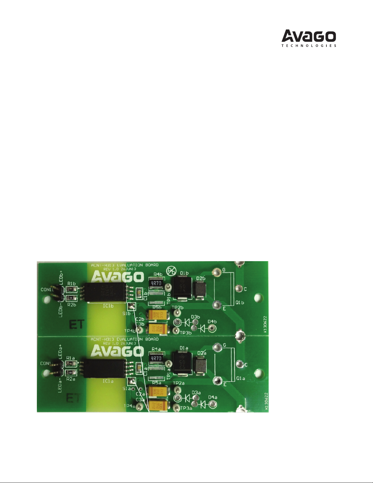
Bootstrapped linkage on solder side (soldered)
S2 on solder side (shorted)S1 (shorted)
Figure 1. Actual ACNT-H313 evaluation board showing default connections
Once inspection is done, the evaluation board can be powered up in four simple steps, according to Figure 2 as shown,
to test either of the top and bottom half-bridge inverter arms in simulation mode without the need of an actual switcher.
Page 2
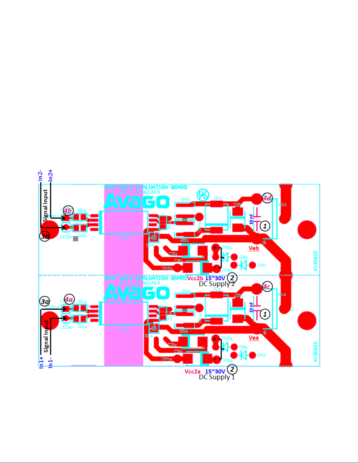
Testing both arms of a half-bridge inverter driver (without a switcher)
1. To simulate the actual gate capacitance of the switcher, solder 10 nF capacitors across Gate and Emitter terminals of
Q1.
2. Connect DC supplies (DC Supplies 1 and 2 with voltage range 15V~30V) across V
of IC1, respectively. For testing, this can be non-isolated.
3. Connect drive signals:
a) A 10 kHz 5 V DC pulse (at slightly < 50% duty) from a dual-output signal generator across the IN1+ and IN1- pins of
CON1a to simulate microcontroller output to drive the lower arm of the half-bridge inverter.
b) Another 10 kHz 5 V DC pulse (at 180° out of phase to 3a) from the dual-output signal generator across IN2+ and IN2-
pins of CON1b to simulate microcontroller output to drive the upper arm of the half-bridge inverter.
4. Use a multi-channel digital oscilloscope to capture the waveforms at the following points:
a. LED signal at IN1+ pin with reference to (w.r.t.) IN1-
b. LED signal at IN2+ pin w.r.t. IN2-
c. Vga representing the output voltage of ACNT-H313 (IC1a) at Gate pin of Q1a w.r.t. V
d. Vgb (through an isolated probe) representing the output voltage of ACNT-H313 (IC1b) at Gate pin of Q1b w.r.t. V
(pin-8) and VEE (pin-5) terminals
CC2
Ea
Eb
Figure 2. Simple simulation test setup of evaluation board
2
Page 3
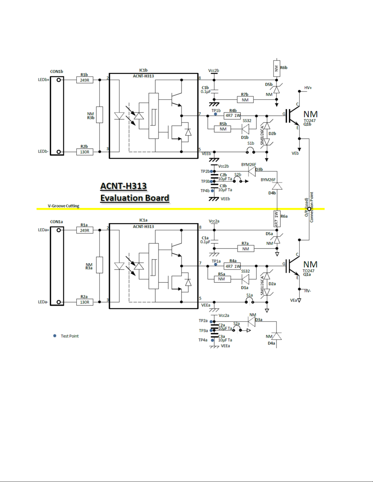
Schematics
Figure 3 shows the schematics of the evaluation board:
Figure 3. Schematics of ACNT-H313 evaluation board
3
Page 4

Practical Connections of the Evaluation Board Using Switchers for Actual Inverter Test
1. Solder actual IGBT or Power MOSFETs at Q1 for the top and bottom arms of the half-bridge inverter isolated drivers.
2. Connect an isolated DC supply 1 (voltage range 15V~30V) across V
for the bottom arm. Then connect another isolated DC supply 2 (voltage range 15V~30V) across V
pin-8 and pin-5 of IC1b, respectively, for the top arm.
3. Connect the signal output (to drive the bottom arm of the half-bridge inverter) from the microcontroller to signal
input 1 across pins IN1+ and IN1- of CON1a of the bottom inverter arm isolated driver.
Connect another signal output (to drive the top arm of the half-bridge inverter) from the microcontroller to signal
input 2 across pins IN2+ and IN2- of CON1b of the top inverter arm isolated driver.
4. Use a multi-channel digital oscilloscope to capture the waveforms at the following points:
a. LED signal at IN1+ pin w.r.t. IN1- for the bottom arm
b. LED signal at IN2+ pin w.r.t. IN2- for the top arm (Note: IN1- and IN2- can be shorted)
c. Vga for the gate driving voltage of Q1a w.r.t. VEa of the bottom inverter arm (dierential probe needed)
d. Vgb for the gate driving voltage of Q1b w.r.t. VEb of the top inverter arm (dierential probe needed)
5. Connect a power cable from the output pin (marked Load) to the inverter load.
6. Connect the high voltage cables from the top arm switcher’s collector pin to HVDC+ and from the bottom arm
switcher’s emitter pin to HVDC-, respectively, as shown. (Note: It is advised that you enable the current-limiting
function of the HV power source supplying the high voltage DC bus voltage during this test to protect the inverter
and its driver circuitries).
CC2a
and V
at pin-8 and pin-5 of IC1a, respectively,
EEa
and V
CC2b
EEb
at
Figure 4. Connection of Evaluation Board in Actual Applications
4
Page 5

Application Circuit Description
The ACNT-H313 is an isolated gate driver that provides 2.5 A output current. The voltage and the high peak output current supplied by this optocoupler make it ideally suited for direct driving of IGBT (or Power MOSFET) with ratings up to
1700 V/100 W. It is also designed to drive dierent sizes of buer stage, which will make the class of switchers scalable.
ACNT-H313 provides a single isolation solution suitable for both low and high power ratings of motor control and inverter applications usually needed in the renewable energy market.
Each of the ACNT-H313 evaluation boards, as shown in Figure 5, accommodates two units of ACNT-H313 ICs. Therefore,
each board is enough to drive the top and bottom arms of the half-bridge inverter. It allows the designer to easily test
the performance of the gate driver in an actual application under real-life operating conditions. Operating the evaluation board requires merely the inclusion of two isolated DC supplies (range 15V~30V) for both arms of inverter switcher,
and provide the necessary PWM drive signals.
Note:
The board shows how the isolation circuitry (at the far left) is easily contained within a small area, while adequate spacing is maintained for good
voltage isolation and easy assembly.
Figure 5. Top and bottom views of ACNT-H313 evaluation board
5
Page 6

Using the Board
The evaluation board is easily prepared for use. Only minor preparations--just by soldering cables for DC supply, proper
cables for HVDC+/HVDC- high voltage bus, and load connections--are required. The evaluation board has a default connection as shown in Table 1 when shipped to the customer, who is free to select dierent power supply schemes.
Power Supply Schemes
The evaluation board is built with DC supply exibility in mind and a total of 4 power supply schemes are possible. Table
1 shows all the possible power supply schemes that work for the evaluation board. A description of each scheme is
given; you are encouraged to explore each scheme and decide which one works best for your needs:
• Scheme 1 is provided by default. As the switchers used are getting bigger, driving power is also bigger. Because a
bootstrapped power supply can handle only lower driving power, it is not suitable for use when Qg of switchers goes
above 200 nC. Two isolated external supplies (+15V~30V for VCC2a and VCC2b) are needed.
• Scheme 2 is the simplest and possibly the cheapest. An external supply (+16V~30V for VCC2a) is needed for the gate
driver driving the switcher at the bottom inverter arm. VCC2b supply (slightly lower in voltage level) is obtained from
VCC2a by bootstrapping operation. For this to work, the bootstrap components D3b, D4b and R6a must be inserted,
all S1 and S2 jumpers must be shorted so that no negative supply of VEE is allowed, and the signal input 2 should be
180o out of phase to signal input 1. (If you require details of bootstrapping operation, contact Avago).
• Scheme 3 is similar to Scheme 1: it uses two external isolated supplies at VCC2a and VCC2b. Scheme 3, however,
has the advantage of getting negative supplies for VEE (or VEEa and VEEb) by introducing a 15 V Zener at D5 and R7
of around 1 kohm to provide proper biasing current at D5. For this scheme to work, all S1 and S2 jumpers must be
open while the external supplies (+18V~30V) are connected across the VCC2 and VEE pins only, not the VE pin. As the
external supply changes from +18 V to +30 V, VCC2 will stay at +15 V, but VEE changes from -3V to -15V, all w.r.t. virtual
ground at VE.
• Scheme 4 is similar to Scheme 3 in that it provides both positive and negative supplies. The dierence, however, is
that all four supplies (two positive supplies for VCC2a and VCC2b, and two negative supplies for VEEa and VEEb) are
provided externally, while VEa and VEb are real grounds. For this scheme to work, all S1 and S2 jumpers must be open.
Table 1.
Power
Supply
V
CC2a
V
EEa
S1a S2a D5a/
R7a
V
CC2b
V
EEb
S1b S2b D5b/
Remarks
R7b
Scheme
1 +15V~30V
External
2 +16V~30V
External
3 +18V~30V External open open 15V/ 1k+18V~30V External open open 15V/ 1kVEE available
15V
4 Dual Supply External open open NM Dual Supply External open open NM VEE available
15V
0 V s/c s/c NM +15V~30V
External
0 V s/c s/c NM
-3V~-15V
-3V~-15V
Bootstrapped
from V
CC2a
(+15V~30V)
15V -3V~-15V
15V
0 V s/c s/c NM Higher Power (Default)
2 external supplies needed for
V
& V
cc2a
cc2b
0 V s/c s/c NM simplest
-3V~-15V
1 external supply needed for
V
cc2a
2 external supplies needed for
V
& V
cc2a
cc2a
& V
cc2b
cc2b
Virtual gnds Vea & Veb generated
thro D5 & R7
2 external supplies needed for
V
Gnds Vea & Veb provided
6
Page 7

Output Measurement
A sample of input LED signals and various output waveforms are captured and shown in Figure 6. The default setup
connection is adopted, but with Q1a and Q1b switchers mounted. The switchers have a gate capacitance equivalent to
10 nF.
Figure 6. Input LED signals and switchers’ gate voltage waveforms
Note: Both IN1+ and IN2+ are set at 49% duty ratio.
Figure 7 shows the turn-o gate signal of Q1a and the turn-on gate signal of Q1b:
Figure 7. Turn-o and Turn-on Gate waveforms of Q1a and Q1b
7
Page 8
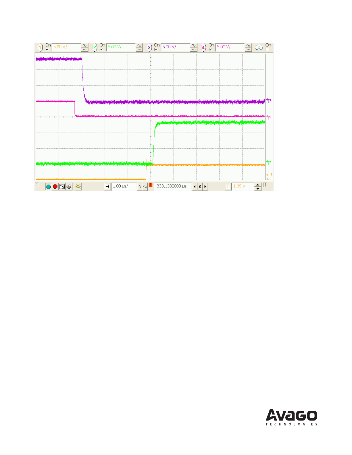
Figure 8 shows the turn-on gate signal of Q1a and the turn-o gate signal of Q1b.
Figure 8. Turn-on and turn-o gate waveforms of Q1a and Q1b
Figure 7 and Figure 8 show that the turn-o speed of the switchers is about 200 ns, due largely to the capacitive eects
of D2 and the gate capacitance of Q1. To improve the turn-o speed, the board is provided with a diode resistor pair
footprints at D1 and R5 (not mounted) to increase the gate current during turn-o. Another way to further improve the
turn-on and turn-o speed is by reducing the gate resistance of R4, but make sure that the gate drive current is not more
than 2.5 A.
For product information and a complete list of distributors, please go to our web site: www.avagotech.com
Avago, Avago Technologies, and the A logo are trademarks of Avago Technologies in the United States and other countries.
Data subject to change. Copyright © 2005-2013 Avago Technologies. All rights reserved.
AV02-4222EN - August 20, 2013
 Loading...