

Page 1

USB-2-I2C
Conversion Kit for HDJD-JD13
Operating Hardware Manual
Introduction
The USB-2-I2C kit is a simple conversion board, which
allows USB connectivity for existing Illumination & Color
Management (ICM) development kit that uses parallel
port interface to connect to an IBM-PC computer. This
conversion board doesn’t need any new USB driver to
work since the driver is come pre-installed in Windows
2000/XP operating system.
The USB-2-I2C conversion kit comes with the following:
• USB-2-I2C Conversion Board (Figure 1-1)
• Parallel port conversion cable
• USB cable
• USB-2-I2C Conversion Kit Operating Hardware Man-
ual
• CMS Program (V1.5.0) for communicating with HDJD-
J822
• CMS Program (V2.1.0) for communicating with ADJD-
J823
If you are missing any part of the kit, please contact your
nearest Avago Technologies sales oce listed in the back
of this publication for help.
USB-2-I2C Conversion Board
The USB-2-I2C conversion board has the following hardware features:
1. USB port and associated hardware for direct connection to an IBM-PC computer USB port
2. 5V to 3.3V voltage level shifter IC
3. Micrcontroller for USB to I2C data transfer
4. Jumper to select either using USB +5V or external
+5V
5. PCB mounting socket for external +5V supply
6. PWM Flex connector that connects to external LED
driver
7. HDJD-JD04 Flex Connector that connect the HDJDJD04 exible circuit board
8. PWM header pin that connects to external LED
driver
9. General purpose external I/O connector to connect to
the unused I/O port of the onboard microcontroller
10. I2C interface that connects to existing ICM development kits that needs USB connectivity. This interface
connects to a parallel port conversion cable.
11. In-circuit programming port for microcontroller
Page 2
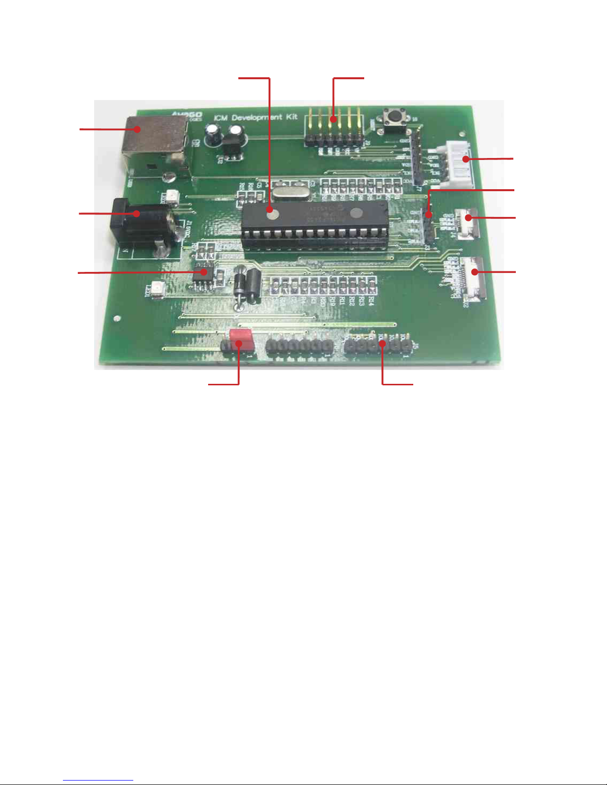
Figure 1. USB-2-I2C Conversion Board
3
2
1
10
4
5
7
6
9
8
11
USB-2-I2C Conversion Kit Hardware User Guide
This guide describes the USB-2-I2C conversion board,
including hardware component layout and schematic.
Chapter 1 : Introduction
• This chapter introduces the USB-2-I2C Conversion Kit
and provides a brief description of the hardware.
Chapter 2 : Hardware Description
• This chapter describes in detail the hardware of the
USB-2-I2C Conversion Board.
Reference Documents
Reference documents listed below are included in the
CD-ROM.
• CMS Program User Guide
(included in the CMS installation program)
• USB-2-I2C User Guide
2
Page 3

Hardware Detail
The USB-2-I2C Conversion Kit hardware is extremely
simple to use and is intended to help user by providing
a tool for user to convert the parallel port based development kit into USB compatible port.
Power Supply
The conversion board is designed to run without any sort
of power supply by harnessing the power from the PC
USB port (+5V). The power port is provided on the board
in case user would like to use an external power supply if
the power requirement is more than 500mA. JP1 is used
to switch between these two form of supply source.
I2C port for parallel cable convertor
This port is hook up with the parallel cable convertor
(included in the kit) to allow user to interface with Avago
Technologies ICM development kit that uses parallel port
interface.
Figure 2. JP1 Power Selector
USB Port
A USB port interface is to provided for easy interfacing
with an IBM-PC computer. The port is used to emulate
I2C communication, using the onboard microcontroller
as the protocol translator. Normal type-B USB cable is
used to hook up the board with the computer.
Onboard I2C Voltage Level Shifter
An onboard voltage level shifter, Philips P82B96, is provided to allow the board to work with dierent I2C bus
voltage.
External Input-Output Connector
Various ports are provided to allow easy interfacing with
additional peripherals (not included with this kit). These
ports include :
• PWM output in header pin and ex-cable connector
(J3/4)
• External I/O pin (J5) for user development purpose
• HDJD-JD04 ex-cable connector (J2) for interfacing
with ADJD-J823 ex-cable version
Figure 3. Parallel Convertor Cable
In-Circuit Serial Programming (ICSP) Connector
By way of the header connector (J9), the PIC18LF2455
protocol translator microcontroller can be connected
for onboard reprogramming. The ICSP connector utilizes
RB6 and RB7 of the microcontrller for in-circuit serial programming. This connector is compatible with Microchip
Promate 2 programmer or ICD-2 in-circuit debugger,
which support ICSP interface.
3
Page 4

USB
Enumeration
Indicator
Power
Indicator
Using USB-2-I2C Conversion Kit (using HDJD-JD13)
The following image illustrates how the conversion
board is connected with Avago Technologies HDJD-JD13
ICM evaluation kit.
Since the parallel conversion cable doesn’t have power
pin, power supply is needed to power up HDJD-JD13 ICM
Evaluation Kit. Make sure the jumper JP1 on USB-2-I2C
conversion board is set to 5VUSB.
Connect the USB cable to an IBM-PC computer USB port.
Once the cable is connected, 2 LED indicators on the
USB-2-I2C should be lighted up. The power indicator will
light up rst follow by the enumeration indicator (usually after 1-2 seconds). When both indicators light up, it
means the USB enumeration on the PC is complete and
the board is ready to use with the CMS software (v1.5.0).
For instruction on how to use CMS software, please refer
to the software guide document that comes with the
CMS software installation program. The document is accesible through the Start Menu -> Program -> CMS 1.5.0
-> Software Guide.
Figure 4. Setup connection for USB-2-I2C with HDJD-JD13
Figure 5. Disconnect state
4
Figure 6. Connect and successful enumeration state
Page 5

Schematic
MC LR1RC 011RC 112RC 213VU SB14RC 4/D -15RC 5/D +16RC 617RC 718OSC 1
9
OSC 2
10
VD D
20
VS S8VS S
19
RA 02RA 13RA 24RA 35RA 46RA 5
7
RB 021RB 122RB 223RB 324RB 425RB 526RB 627RB 7
28
U1
PIC 18LF 2455
R1
470R
C1
0.1uF
R2
10k
1 4
2 3
S1
VC C
C2
0.1uF
Y 1
20MHz
C3
22pF
C4
22pF
123
4
5
CN1
CN-U SB
R3
27RR427R
C5
0.1uF
C11
10nF
L1
FE RR IT E
R5
470R
LE D2
GR N
R6 0R
R7 0R
R8 0R
R9 0R
R10 0R
R11 0R
R12 0R
R13 0R
R14 0R
SC L
SDA
VP
D1
1N4001
R15
100k
R16
100k
VU SB
VU SB
12345
6
J9
IC SP (R PIN)
VP
VC C
Tx3Rx2Ty
5
GN D
4
Sx
1
Sy
7
Ry
6
V CC
8
U3
P82B96T
R18
2k7
R17
2k7
C5
0.1uF
R19
2k7
R20
2k7
C6
1uF
3.3V
C7
1uF
3.3V
VC C3.3V
1
2
J1
PWR (SOC KE T)
123456789
10
J2
SY S (F LE X)
VC C
SL EE P
MR
MR
SL EE P
PWMR
PWMG
PWMB
123
4
J3
PWM ( PIN)
123
4
J4
PWM ( FL EX )
123
4
J8
I2C ( JST )
SC L5V
SDA5V
VC C
12345
6
J7
I2C ( PIN)
VC C
SDA
SC LMRSL EE P
12345
6
J6
PWR (PIN )
GND
GND
IO0
IO1
IO2
IO3
IO4
IO5
12345
6
J5
IO ( PIN)
IO0
IO1
IO2
IO3
IO4
IO5
5VNCSDA
SC L
SL EE PMRPWMR
PWMG
PWMB
GND
PWMR
PWMG
PWMB
GND
PWMR
PWMG
PWMB
GND
VC C
SC L
SDA
GND
VC C
SC L
SDA
SL EE PMRGND
5V5V3.3V
3.3V
GND
GND
I/O0
I/O1
I/O2
I/O3
I/O4
I/O5
321
JP1
PWR SE LE CTOR
VC C 3.3V
R21
470R
LE D1
GR N
USB OK
Vi n
1
GN D
2
Vout
3
U2
LE 33
SCL5V
SDA5V
The following gure shows the schematic of the USB-2-I2C Conversion Board.
Figure 7. USB-2-I2C conversion board schematic
5
Page 6

For product information and a complete list of distributors, please go to our web site: www.avagotech.com
Avago, Avago Technologies, and the A logo are trademarks of Avago Technologies, Limited in the United States and other countries.
Data subject to change. Copyright © 2007 Avago Technologies Limited. All rights reserved.
AV02-0065EN - January 9, 2007
 Loading...