


HSMS-282x
COMMON
CATHODE
#4
UNCONNECTED
PAIR
#5
COMMON
ANODE
#3
SERIES
#2
SINGLE
#0
1 2
3
1 2
3 4
RING
QUAD
#7
1 2
3 4
BRIDGE
QUAD
#8
1 2
3 4
CROSS-OVER
QUAD
#9
1 2
3 4
1 2
3
1 2
3
1 2
3
COMMON
CATHODE
F
COMMON
ANODE
E
SERIES
C
SINGLE
B
COMMON
CATHODE QUAD
M
UNCONNECTED
TRIO
L
BRIDGE
QUAD
P
COMMON
ANODE QUAD
N
RING
QUAD
R
1 2 3
6 5 4
HIGH ISOLATION
UNCONNECTED PAIR
K
1 2 3
6 5 4
1 2 3
6 5 4
1 2 3
6 5 4
1 2 3
6 5 4
1 2 3
6 5 4
Surface Mount RF Schottky Barrier Diodes
Data Sheet
Description/Applications
These Schottky diodes are specically designed for both
analog and digital applications. This series oers a wide
range of specications and package congurations to give
the designer wide exibility. Typical applications of these
Schottky diodes are mixing, detecting, switching, sam‑
pling, clamping, and wave shaping. The HSMS‑282x series
of diodes is the best all‑around choice for most applica‑
tions, featuring low series resistance, low forward voltage
at all current levels and good RF characteristics.
Note that Avago’s manufacturing techniques assure that
dice found in pairs and quads are taken from adjacent
sites on the wafer, assuring the highest degree of match.
Package Lead Code Identication,
SOT-23/SOT-143 (Top View)
Features
• Low Turn‑On Voltage (As Low as 0.34 V at 1 mA)
• Low FIT (Failure in Time) Rate*
• Six‑sigma Quality Level
• Single, Dual and Quad Versions
• Unique Congurations in Surface Mount SOT‑363
Package
– increase exibility
– save board space
– reduce cost
• HSMS‑282K Grounded Center Leads Provide up to 10
dB Higher Isolation
• Matched Diodes for Consistent Performance
• Better Thermal Conductivity for Higher Power Dissipation
• Lead‑free Option Available
• For more information see the Surface Mount Schottky
Reliability Data Sheet.
Package Lead Code Identication, SOT-363
Package Lead Code Identication, SOT-323
(Top View)
(Top View)

Pin Connections and Package Marking
GUx
1
2
3
6
5
4
Notes:
1. Package marking provides orientation and identication.
2. See “Electrical Specications” for appropriate package marking.
Absolute Maximum Ratings
[1]
TC = 25°C
Symbol Parameter Unit SOT-23/SOT-143 SOT-323/SOT-363
If Forward Current (1 μs Pulse) Amp 1 1
PIV Peak Inverse Voltage V 15 15
Tj Junction Temperature °C 150 150
T
Storage Temperature °C ‑65 to 150 ‑65 to 150
stg
θjc Thermal Resistance
Notes:
1. Operation in excess of any one of these conditions may result in permanent damage to the device.
2. TC = +25°C, where TC is dened to be the temperature at the package pins where contact is made to the circuit board.
Electrical Specications TC = 25°C, Single Diode
[2]
°C/W 500 150
[3]
Maximum Maximum
Minimum Maximum Forward Reverse Typical
Part Package Breakdown Forward Voltage Leakage Maximum Dynamic
Number Marking Lead Voltage Voltage VF (V) @ IR (nA) @ Capacitance Resistance
[4]
HSMS
Code Code Conguration VBR (V) VF (mV) IF (mA) VR (V) CT (pF) RD (Ω)
2820 C0 0 Single 15 340 0.5 10 100 1 1.0 12
2822 C2 2 Series
2823 C3 3 Common Anode
2824 C4 4 Common Cathode
2825 C5 5 Unconnected Pair
2827 C7 7 Ring Quad
2828 C8 8 Bridge Quad
[4]
[4]
2829 C9 9 Cross‑over Quad
282B C0 B Single
282C C2 C Series
282E C3 E Common Anode
282F C4 F Common Cathode
282K CK K High Isolation
Unconnected Pair
282L CL L Unconnected Trio
282M HH M Common Cathode Quad
282N NN N Common Anode Quad
282P CP P Bridge Quad
282R OO R Ring Quad
Test Conditions IR = 100 mA IF = 1 mA
[1]
VR = 0V
[2]
I
f = 1 MHz
= 5 mA
F
[5]
Notes:
1. ∆VF for diodes in pairs and quads in 15 mV maximum at 1 mA.
2. ∆CTO for diodes in pairs and quads is 0.2 pF maximum.
3. Eective Carrier Lifetime (τ) for all these diodes is 100 ps maximum measured with Krakauer method at 5 mA.
4. See section titled “Quad Capacitance.”
5. RD = RS + 5.2Ω at 25°C and If = 5 mA.
2
Quad Capacitance
C
1
x C
2
C3 x C
4
C
DIAGONAL
= _______ + _______
C
1
+ C2 C3 + C
4
C
1
x C
2
C3 x C
4
C
DIAGONAL
= _______ + _______
C
1
+ C2 C3 + C
4
1
C
ADJACENT
= C1 + ____________
1 1 1
–– + –– + ––
C2 C3C
4
C
1
C
2
C
4
C
3
A
B
C
j
R
j
R
S
Rj =
8.33 X 10⁻⁵ nT
Ib + I
s
where
Ib = externally applied bias current in amps
Is = saturation current (see table of SPICE parameters)
T = temperature, °K
n = ideality factor (see table of SPICE parameters)
Note:
To effectively model the packaged HSMS-282x product,
please refer to Application Note AN1124.
RS = series resistance (see Table of SPICE parameters)
Cj = junction capacitance (see Table of SPICE parameters)
Capacitance of Schottky diode quads is measured using
an HP4271 LCR meter. This instrument eectively isolates
individual diode branches from the others, allowing ac‑
curate capacitance measurement of each branch or each
diode. The conditions are: 20 mV R.M.S. voltage at 1 MHz.
Avago denes this measurement as “CM”, and it is equiva‑
lent to the capacitance of the diode by itself. The equiva‑
lent diagonal and adjacent capaci‑tances can then be cal‑
culated by the formulas given below.
In a quad, the diagonal capacitance is the capacitance be‑
tween points A and B as shown in the gure below. The
diagonal capacitance is calculated using the following
formula
The equivalent adjacent capacitance is the capacitance
between points A and C in the gure below. This capaci‑
tance is calculated using the following formula
Linear Equivalent Circuit Model Diode Chip
ESD WARNING:
Handling Precautions Should Be Taken To Avoid Static Discharge.
This information does not apply to cross‑over quad di‑
odes.
3
SPICE Parameters
Parameter Units HSMS-282x
BV V 15
CJ0 pF 0.7
EG eV 0.69
IBV A 1E‑4
IS A 2.2E‑8
N 1.08
RS Ω 6.0
PB V 0.65
PT 2
M 0.5

Typical Performance, TC = 25°C (unless otherwise noted), Single Diode
Figure 1. Forward Current vs. Forward Voltage at
Temperatures.
0 0.10 0.20 0.30 0.500.40
I
F
– FORWARD CURRENT (mA)
VF – FORWARD VOLTAGE (V)
0.01
10
1
0.1
100
TA = +125C
TA = +75C
TA = +25C
TA = –25C
Figure 2. Reverse Current vs. Reverse Voltage at
Temperatures.
0 5 15
I
R
– REVERSE CURRENT (nA)
VR – REVERSE VOLTAGE (V)
10
1
1000
100
10
100,000
10,000
TA = +125C
TA = +75C
TA = +25C
Figure 3. Total Capacitance vs. Reverse Voltage.
0 2 86
C
T
– CAPACITANCE (pF)
VR – REVERSE VOLTAGE (V)
4
0
0.6
0.4
0.2
1
0.8
Figure 4. Dynamic Resistance vs. Forward
Current.
0.1 1 100
R
D
– DYNAMIC RESISTANCE ()
IF – FORWARD CURRENT (mA)
10
1
10
1000
100
VF - FORWARD VOLTAGE (V)
Figure 5. Typical Vf Match, Series Pairs and Quads
at Mixer Bias Levels.
30
10
1
0.3
30
10
1
0.3
I
F
- FORWARD CURRENT (mA)
V
F
- FORWARD VOLTAGE DIFFERENCE (mV)
0.2 0.4 0.6 0.8 1.0 1.2 1.4
IF (Left Scale)
VF (Right Scale)
VF - FORWARD VOLTAGE (V)
Figure 6. Typical Vf Match, Series Pairs at Detector
Bias Levels.
100
10
1
1.0
0.1
I
F
- FORWARD CURRENT (µA)
V
F
- FORWARD VOLTAGE DIFFERENCE (mV)
0.10 0.15 0.20 0.25
IF (Left Scale)
VF (Right Scale)
Figure 7. Typical Output Voltage vs. Input Power,
Small Signal Detector Operating at 850 MHz.
-40 -30
18 nH
RF in
3.3 nH
100 pF
100 K
HSMS-282B
Vo
0
V
O
– OUTPUT VOLTAGE (V)
Pin – INPUT POWER (dBm)
-10-20
0.001
0.01
1
0.1
-25C
+25C
+75C
DC bias = 3 A
Figure 8. Typical Output Voltage vs. Input Power,
Large Signal Detector Operating at 915 MHz.
-20 -10
RF in
100 pF
4.7 K
68
HSMS-282B
Vo
30
V
O
– OUTPUT VOLTAGE (V)
Pin – INPUT POWER (dBm)
10 200
1E-005
0.0001
0.001
10
0.1
1
0.01
+25C
LOCAL OSCILLATOR POWER (dBm)
Figure 9. Typical Conversion Loss vs. L.O. Drive,
2.0 GHz (Ref AN997).
CONVERSION LOSS (dB)
12
10
9
8
7
6
20 6 8 104
4

Applications Information
8.33 X 10⁻⁵ nT
Rj = –––––––––––– = RV– R
s
IS + I
b
0.026
≈ ––––– at 25 °C
IS + I
b
8.33 X 10⁻⁵ nT
Rj = –––––––––––– = RV– R
s
IS + I
b
0.026
≈ ––––– at 25 °C
IS + I
b
V - IR
S
I = IS (e
–––––
– 1)
0.026
R
S
R
j
C
j
METAL
SCHOTTKY JUNCTION
PASSIVATION PASSIVATION
N-TYPE OR P-TYPE EPI LAYER
N-TYPE OR P-TYPE SILICON SUBSTRATE
CROSS-SECTION OF SCHOTTKY
BARRIER DIODE CHIP
EQUIVALENT
CIRCUIT
Product Selection
Avago’s family of surface mount Schottky diodes provide
unique solutions to many design problems. Each is opti‑
mized for certain applications.
The rst step in choosing the right product is to select
the diode type. All of the products in the HSMS‑282x fam‑
ily use the same diode chip–they dier only in package
conguration. The same is true of the HSMS‑280x, ‑281x,
285x, ‑286x and ‑270x families. Each family has a dierent
set of characteristics, which can be compared most easily
by consulting the SPICE parameters given on each data
sheet.
The HSMS‑282x family has been optimized for use in RF
applications, such as
• DC biased small signal detectors to 1.5 GHz.
• Biased or unbiased large signal detectors (AGC or
power monitors) to 4 GHz.
• Mixers and frequencymultipliers to 6 GHz.
The other feature of the HSMS‑282x family is its unit‑to‑unit
and lot‑to‑lot consistency. The silicon chip used in this
series has been designed to use the fewest possible pro‑
cessing steps to minimize variations in diode characteris‑
tics. Statistical data on the consistency of this product, in
terms of SPICE parameters, is available from Avago.
where
n = ideality factor (see table of SPICE parameters)
T = temperature in °K
IS = saturation current (see table of SPICE parameters)
Ib = externally applied bias current in amps
Rv = sum of junction and series resistance, the slope of the
V‑I curve
IS is a function of diode barrier height, and can range from
picoamps for high barrier diodes to as much as 5 µA for
very low barrier diodes.
The Height of the Schottky Barrier
The current‑voltage characteristic of a Schottky barrier
diode at room temperature is described by the following
equation:
For those applications requiring very high breakdown
voltage, use the HSMS‑280x family of diodes. Turn to the
HSMS‑281x when you need very low icker noise. The
HSMS‑285x is a family of zero bias detector diodes for small
signal applications. For high frequency detector or mixer
applications, use the HSMS‑286x family. The HSMS‑270x
is a series of specialty diodes for ultra high speed clipping
and clamping in digital circuits.
Schottky Barrier Diode Characteristics
Stripped of its package, a Schottky barrier diode chip
consists of a metal‑semiconductor barrier formed by de‑
position of a metal layer on a semiconductor. The most
common of several dierent types, the passivated diode,
is shown in Figure 10, along with its equivalent circuit.
RS is the parasitic series resistance of the diode, the sum
of the bondwire and leadframe resistance, the resistance
of the bulk layer of silicon, etc. RF energy coupled into RS
is lost as heat—it does not contribute to the rectied out‑
put of the diode. CJ is parasitic junction capacitance of the
diode, controlled by the thick‑ness of the epitaxial layer
and the diameter of the Schottky contact. Rj is the junc‑
tion resistance of the diode, a function of the total current
owing through it.
5
On a semi‑log plot (as shown in the Avago catalog) the
current graph will be a straight line with inverse slope 2.3
X 0.026 = 0.060 volts per cycle (until the eect of RS is seen
in a curve that droops at high current). All Schottky diode
curves have the same slope, but not necessarily the same
value of current for a given voltage. This is determined
by the saturation current, IS, and is related to the barrier
height of the diode.
Through the choice of p‑type or n‑type silicon, and the
selection of metal, one can tailor the characteristics of a
Schottky diode. Barrier height will be altered, and at the
same time CJ and RS will be changed. In general, very low
barrier height diodes (with high values of IS, suitable for
zero bias applications) are realized on p‑type silicon. Such
diodes suer from higher values of RS than do the n‑type.
Figure 10. Schottky Diode Chip.

DC Bias
DC Biased DiodesZero Biased Diodes
Thus, p‑type diodes are generally reserved for detector
DC Bias
Shunt inductor provides
video signal return
Shunt diode provides
video signal return
DC Bias
DC Biased DiodesZero Biased Diodes
differential
amplifier
R
L
Video out
+3V
RF in
R
L
R
M
RF
impedance
matching
network
applications (where very high values of RV swamp out
high RS) and n‑type diodes such as the HSMS‑282x are
used for mixer applications (where high L.O. drive levels
keep RV low). DC biased detectors and self‑biased detec‑
tors used in gain or power control circuits.
Detector Applications
Detector circuits can be divided into two types, large signal
(Pin > ‑20 dBm) and small signal (Pin < ‑20 dBm). In general,
the former use resistive impedance matching at the in‑
put to improve atness over frequency —this is possible
since the input signal levels are high enough to produce
adequate output voltages without the need for a high Q
reactive input matching network. These circuits are self‑
biased (no external DC bias) and are used for gain and
power control of ampliers.
Small signal detectors are used as very low cost receivers,
and require a reactive input impedance matching net‑
work to achieve adequate sensitivity and output voltage.
Those operating with zero bias utilize the HSMS‑ 285x
family of detector diodes. However, superior performance
over temperature can be achieved with the use of 3 to 30
µA of DC bias. Such circuits will use the HSMS‑282x family
of diodes if the operating frequency is 1.5 GHz or lower.
Typical performance of single diode detectors (using
HSMS‑2820 or HSMS‑282B) can be seen in the transfer
curves given in Figures 7 and 8. Such detectors can be re‑
alized either as series or shunt circuits, as shown in Figure
11.
• The two diodes are in parallel in the RF circuit, lowering
the input impedance and making the design of the RF
matching network easier.
• The two diodes are in series in the output (video) circuit,
doubling the output voltage.
• Some cancellation of even‑order harmonics takes place
at the input.
Figure 12. Voltage Doubler.
The most compact and lowest cost form of the doubler is
achieved when the HSMS‑2822 or HSMS‑282C series pair
is used.
Both the detection sensitivity and the DC forward voltage
of a biased Schottky detector are temperature sensitive.
Where both must be compensated over a wide range of
temperatures, the dierential detector
[2]
is often used.
Such a circuit requires that the detector diode and the
reference diode exhibit identical characteristics at all DC
bias levels and at all temperatures. This is accomplished
through the use of two diodes in one package, for exam‑
ple the HSMS‑2825 in Figure 13. In the Avago assembly
facility, the two dice in a surface mount package are taken
from adjacent sites on the wafer (as illustrated in Figure
14). This assures that the characteristics of the two diodes
are more highly matched than would be possible through
individual testing and hand matching.
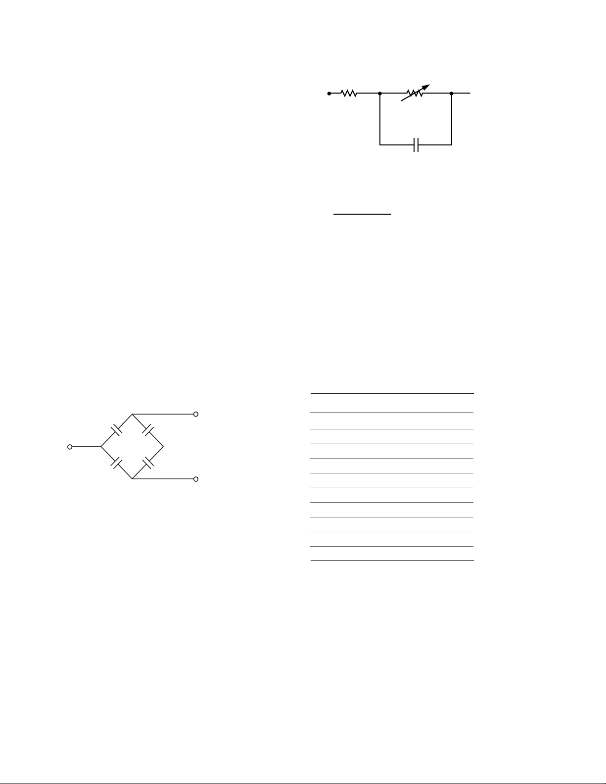
Figure 11. Single Diode Detectors.
The series and shunt circuits can be combined into a volt‑
age doubler
three advantages over the single diode circuit.
6
Figure 13. Dierential Detector.
[1]
, as shown in Figure 12. The doubler oers
[1] Avago Application Note 956‑4, “Schottky Diode Voltage Doubler.”
[2] Raymond W. Waugh, “Designing Large‑Signal Detectors for Handsets
and Base Stations,” Wireless Systems Design, Vol. 2, No. 7, July 1997,
pp 42 – 48.

Figure 14. Fabrication of Avago Diode Pairs.
PA
detector diode
reference diode
to differential amplifier
V
bias
HSMS-282K
matching
network
differential
amplifier
HSMS-2825
HSMS-2825
bias
differential
amplifier
HSMS-282P
bias
matching
network
RF
in
V
o
D1
33 pF
HSMS-2825
or
HSMS-282K
HSMS-282K
4.7 KΩ
33 pF
4.7 KΩ
4.7 KΩ
D2
68 Ω
68 Ω
RF
in
V
o
Figure 17. Voltage Doubler Dierential Detector.
In high power applications, coupling of RF energy from
the detector diode to the reference diode can introduce
error in the dierential detector. The HSMS‑282K diode
pair, in the six lead SOT‑363 package, has a copper bar
between the diodes that adds 10 dB of additional isola‑
tion between them. As this part is manufactured in the
SOT‑363 package it also provides the benet of being
40% smaller than larger SOT‑143 devices. The HSMS‑282K
is illustrated in Figure 15 — note that the ground connec‑
tions must be made as close to the package as possible to
minimize stray inductance to ground.
However, care must be taken to assure that the two refer‑
ence diodes closely match the two detector diodes. One
possible conguration is given in Figure 16, using two
HSMS‑2825. Board space can be saved through the use of
the HSMS‑282P open bridge quad, as shown in Figure 17.
While the dierential detector works well over tempera‑
ture, another design approach
[3]
works well for large signal
detectors. See Figure 18 for the schematic and a physical
layout of the circuit. In this design, the two 4.7 KΩ resis‑
tors and diode D2 act as a variable power divider, assuring
constant output voltage over temperature and improving
output linearity.
Figure 15. High Power Dierential Detector.
The concept of the voltage doubler can be applied to the
Figure 18. Temperature Compensated Detector.
dierential detector, permitting twice the output voltage
for a given input power (as well as improving input im‑
pedance and suppressing second harmonics).
In certain applications, such as a dual‑band cellphone
handset operating at both 900 and 1800 MHz, the second
harmonics generated in the power control output detec‑
tor when the handset is working at 900 MHz can cause
problems. A lter at the output can reduce unwanted
emissions at 1800 MHz in this case, but a lower cost so‑
lution is available
[4]
. Illustrated schematically in Figure
19, this circuit uses diode D2 and its associated passive
components to cancel all even order harmonics at the
detector’s RF input. Diodes D3 and D4 provide tempera‑
ture compensation as described above. All four diodes are
contained in a single HSMS‑ 282R package, as illustrated
7
Figure 16. Voltage Doubler Dierential Detector.
in the layout shown in Figure 20.
[3] Hans Eriksson and Raymond W. Waugh, “A Temperature Compensated
Linear Diode Detector,” to be published.

RF in
D1
R1 V+
R2
D3
C1V–
R4
D4
C1 = C2 ≈ 100 pF
R1 = R2 = R3 = R4 = 4.7 KΩ
D1 & D2 & D3 & D4 = HSMS-282R
C2
D2
68 Ω
R3
Figure 19. Schematic of Suppressed Harmonic Detector.
HSMS-282R
4.7 KΩ
4.7 KΩ
100 pF
100 pF
68 Ω
V–
RF in
V+
HSMS-282R
IF out
RF in
LO in
HSMS-2829
IF out
RF in
LO in
HSMS-282R
IF out
RF in
LO in
HSMS-282R
180°
hybrid
IF out
LO in
RF in
Low pass
filter
Figure 20. Layout of Suppressed Harmonic Detector.
Note that the forgoing discussion refers to the output volt‑
age being extracted at point V+ with respect to ground. If
a dierential output is taken at V+ with respect to V‑, the
circuit acts as a voltage doubler.
Mixer applications
The HSMS‑282x family, with its wide variety of packaging,
can be used to make excellent mixers at frequencies up
to 6 GHz.
The HSMS‑2827 ring quad of matched diodes (in the SOT‑143
package) has been designed for double balanced mixers.
The smaller (SOT‑363) HSMS‑282R ring quad can similarly
be used, if the quad is closed with external connections as
shown in Figure 21.
Figure 22. Planar Double Balanced Mixer.
A review of Figure 21 may lead to the question as to why
the HSMS‑282R ring quad is open on the ends. Distor‑
tion in double balanced mixers can be reduced if LO drive
is increased, up to the point where the Schottky diodes
are driven into saturation. Above this point, increased LO
drive will not result in improvements in distortion. The use
of expensive high barrier diodes (such as those fabricated
on GaAs) can take advantage of higher LO drive power,
but a lower cost solution is to use a eight (or twelve) diode
ring quad. The open design of the HSMS‑282R permits this
to easily be done, as shown in Figure 23.
Figure 23. Low Distortion Double Balanced Mixer.
This same technique can be used in the single‑balanced
mixer. Figure 24 shows such a mixer, with two diodes in
each spot normally occupied by one. This mixer, with a
suciently high LO drive level, will display low distortion.
Figure 21. Double Balanced Mixer.
Both of these networks require a crossover or a three di‑
mensional circuit. A planar mixer can be made using the
SOT‑143 crossover quad, HSMS‑2829, as shown in Figure
22. In this product, a special lead frame permits the cross‑
over to be placed inside the plastic package itself, elimi‑
nating the need for via holes (or other measures) in the RF
portion of the circuit itself.
8
Figure 24. Low Distortion Balanced Mixer.
[4] Alan Rixon and Raymond W. Waugh, “A Suppressed Harmonic Power
Detector for Dual Band ‘Phones,” to be published.

Sampling Applications
HSMS-282P
sampling
pulse
sample
point
sampling circuit
11600 (Vf– If Rs)
nT
If = IS e – 1
11600 (Vf– If Rs)
nT
If = IS e – 1
2 1 1
n
– 4060 (
T– 298
)
Is= I
0
(
T
)
e
298
The six lead HSMS‑282P can be used in a sampling circuit,
as shown in Figure 25. As was the case with the six lead
HSMS‑282R in the mixer, the open bridge quad is closed
with traces on the circuit board. The quad was not closed
internally so that it could be used in other applications,
such as illustrated in Figure 17.
Figure 25. Sampling Circuit.
Thermal Considerations
The obvious advantage of the SOT‑323 and SOT‑363 over
the SOT‑23 and SOT‑142 is combination of smaller size
and extra leads. However, the copper leadframe in the
SOT‑3x3 has a thermal conductivity four times higher than
the Alloy 42 leadframe of the SOT‑23 and SOT‑143, which
enables the smaller packages to dissipate more power.
The maximum junction temperature for these three fami‑
lies of Schottky diodes is 150°C under all operating con‑
ditions. The following equation applies to the thermal
analysis of diodes:
Note that θjc, the thermal resistance from diode junction
to the foot of the leads, is the sum of two component re‑
sistances,
θjc = θ
pkg
+ θ
(2)
chip
Package thermal resistance for the SOT‑3x3 package is ap‑
proximately 100°C/W, and the chip thermal resistance for
the HSMS‑282x family of diodes is approximately 40°C/W.
The designer will have to add in the thermal resistance
from diode case to ambient— a poor choice of circuit
board material or heat sink design can make this number
very high.
Equation (1) would be straightforward to solve but for the
fact that diode forward voltage is a function of tempera‑
ture as well as forward current. The equation for Vf is:
(3)
where
n = ideality factor
T = temperature in °K
Rs = diode series resistance
and IS (diode saturation current) is given by
Tj = (Vf If + PRF) θjc + Ta (1)
where
Tj = junction temperature
Ta = diode case temperature
θjc = thermal resistance
VfIf = DC power dissipated
PRF = RF power dissipated
(4)
Equation (4) is substituted into equation (3), and equa‑
tions (1) and (3) are solved simultaneously to obtain the
value of junction temperature for given values of diode
case temperature, DC power dissipation and RF power
dissipation.
9

0.026
0.039
0.079
0.022
Dimensions in inches
0.026
0.079
0.018
0.039
Dimensions in inches
Diode Burnout
Assembly Instructions
Any Schottky junction, be it an RF diode or the gate of a
MESFET, is relatively delicate and can be burned out with
excessive RF power. Many crystal video receivers used
in RFID (tag) applications nd themselves in poorly con‑
trolled environments where high power sources may
be present. Examples are the areas around airport and
FAA radars, nearby ham radio operators, the vicinity of a
broadcast band transmitter, etc. In such environments,
the Schottky diodes of the receiver can be protected by a
device known as a limiter diode.
[5]
Formerly available only
in radar warning receivers and other high cost electronic
warfare applications, these diodes have been adapted to
commercial and consumer circuits.
Avago oers a complete line of surface mountable PIN
limiter diodes. Most notably, our HSMP‑4820 (SOT‑23) can
act as a very fast (nanosecond) power‑sensitive switch
when placed between the antenna and the Schottky di‑
ode, shorting out the RF circuit temporarily and reecting
the excessive RF energy back out the antenna.
[5] Avago Application Note 1050, “Low Cost, Surface Mount Power
Limiters.”
SOT-3x3 PCB Footprint
Recommended PCB pad layouts for the miniature SOT‑
3x3 (SC‑70) packages are shown in Figures 26 and 27 (di‑
mensions are in inches). These layouts provide ample al‑
lowance for package placement by automated assembly
equipment without adding parasitics that could impair
the performance.
Figure 26. Recommended PCB Pad Layout for Avago’s SC70 3L/SOT-323 Products.
10
Figure 27. Recommended PCB Pad Layout for Avago's SC70 6L/SOT-363 Products.

25
Time
Temperature
Tp
T
L
tp
t
L
t 25° C to Peak
Ramp-up
ts
Ts
min
Ramp-down
Preheat
Critical Zone
T
L
to Tp
Ts
max
SMT Assembly
Reliable assembly of surface mount components is a com‑
plex process that involves many material, process, and
equipment factors, including: method of heating (e.g., IR
or vapor phase reow, wave soldering, etc.) circuit board
material, conductor thickness and pattern, type of solder
alloy, and the thermal conductivity and thermal mass of
components. Components with a low mass, such as the
SOT packages, will reach solder reow temperatures fast‑
er than those with a greater mass.
Avago’s diodes have been qualied to the time‑tempera‑
ture prole shown in Figure 28. This prole is representa‑
tive of an IR reow type of surface mount assembly pro‑
cess.
After ramping up from room temperature, the circuit
board with components attached to it (held in place with
solder paste) passes through one or more preheat zones.
The preheat zones increase the temperature of the board
and components to prevent thermal shock and begin
evaporating solvents from the solder paste. The reow
zone briey elevates the temperature suciently to pro‑
duce a reow of the solder.
The rates of change of temperature for the ramp‑up and
cool‑down zones are chosen to be low enough to not
cause deformation of the board or damage to compo‑
nents due to thermal shock. The maximum temperature
in the reow zone (T
) should not exceed 260°C.
MAX
These parameters are typical for a surface mount assem‑
bly process for Avago diodes. As a general guideline, the
circuit board and components should be exposed only
to the minimum temperatures and times necessary to
achieve a uniform reow of solder.
Figure 28. Surface Mount Assembly Prole.
Lead-Free Reow Prole Recommendation (IPC/JEDEC J-STD-020C)
Reow Parameter Lead-Free Assembly
Average ramp‑up rate (Liquidus Temperature (T
Preheat Temperature Min (T
Temperature Max (T
Time (min to max) (tS) 60‑180 seconds
11
Ts(max) to TL Ramp‑up Rate 3°C/second max
Time maintained above: Temperature (TL) 217°C
Peak Temperature (TP) 260 +0/‑5°C
Time within 5 °C of actual
Peak temperature (tP)
Ramp‑down Rate 6°C/second max
Time 25 °C to Peak Temperature 8 minutes max
Note 1: All temperatures refer to topside of the package, measured on the package body surface
Time (tL) 60‑150 seconds
to Peak) 3°C/ second max
S(max)
) 150°C
S(min)
) 200°C
S(max)
20‑40 seconds

Package Dimensions
e
B
e2
e1
E1
C
E
XXX
L
D
A
A1
Notes:
XXX-package marking
Drawings are not to scale
DIMENSIONS (mm)
MIN.
0.79
0.000
0.30
0.08
2.73
1.15
0.89
1.78
0.45
2.10
0.45
MAX.
1.20
0.100
0.54
0.20
3.13
1.50
1.02
2.04
0.60
2.70
0.69
SYMBOL
A
A1
B
C
D
E1
e
e1
e2
E
L
e
B
e2
B1
e1
E1
C
E
XXX
L
D
A
A1
Notes:
XXX-package marking
Drawings are not to scale
DIMENSIONS (mm)
MIN.
0.79
0.013
0.36
0.76
0.086
2.80
1.20
0.89
1.78
0.45
2.10
0.45
MAX.
1.097
0.10
0.54
0.92
0.152
3.06
1.40
1.02
2.04
0.60
2.65
0.69
SYMBOL
A
A1
B
B1
C
D
E1
e
e1
e2
E
L
e
B
e1
E1
C
E
XXX
L
D
A
A1
Notes:
XXX-package marking
Drawings are not to scale
DIMENSIONS (mm)
MIN.
0.80
0.00
0.15
0.08
1.80
1.10
1.80
0.26
MAX.
1.00
0.10
0.40
0.25
2.25
1.40
2.40
0.46
SYMBOL
A
A1
B
C
D
E1
e
e1
E
L
1.30 typical
0.65 typical
E
HE
D
e
A1
b
A
A2
L
c
DIMENSIONS (mm)
MIN.
1.15
1.80
1.80
0.80
0.80
0.00
0.15
0.08
0.10
MAX.
1.35
2.25
2.40
1.10
1.00
0.10
0.30
0.25
0.46
SYMBOL
E
D
HE
A
A2
A1
e
b
c
L
0.650 BCS
Outline 23 (SOT-23)
Outline SOT-323 (SC-70 3 Lead)
Outline 143 (SOT-143) Outline SOT-363 (SC-70 6 Lead)
12
Device Orientation
USER
FEED
DIRECTION
COVER TAPE
CARRIER
TAPE
REEL
Note: "AB" represents package marking code.
"C" re
p
resents date code.
END VIEW
8 mm
4 mm
TOP VIEW
ABC ABC ABC ABC
Note: "AB" represents package marking code.
"C" represents date code.
END VIEW
8 mm
4 mm
TOP VIEW
ABC ABC ABC ABC
END VIEW
8 mm
4 mm
TOP VIEW
Note: "AB" represents package marking code.
"C" represents date code.
ABC ABC ABC ABC
For Outlines SOT-23, -323
For Outline SOT-143
For Outline SOT-363
13
9° MAX
A
0
P
P
0
D
P
2
E
F
W
D
1
Ko
8° MAX
B
0
13.5° MAX
t1
DESCRIPTION SYMBOL SIZE (mm) SIZE (INCHES)
LENGTH
WIDTH
DEPTH
PITCH
BOTTOM HOLE DIAMETER
A
0
B
0
K
0
P
D
1
3.15 ± 0.10
2.77 ± 0.10
1.22 ± 0.10
4.00 ± 0.10
1.00 + 0.05
0.124 ± 0.004
0.109 ± 0.004
0.048 ± 0.004
0.157 ± 0.004
0.039 ± 0.002
CAVITY
DIAMETER
PITCH
POSITION
D
P
0
E
1.50 + 0.10
4.00 ± 0.10
1.75 ± 0.10
0.059 + 0.004
0.157 ± 0.004
0.069 ± 0.004
PERFORATION
WIDTH
THICKNESS
Wt18.00 + 0.30 – 0.10
0.229 ± 0.013
0.315 + 0.012 – 0.004
0.009 ± 0.0005
CARRIER TAPE
CAVITY TO PERFORATION
(WIDTH DIRECTION)
CAVITY TO PERFORATION
(LENGTH DIRECTION)
F
P
2
3.50 ± 0.05
2.00 ± 0.05
0.138 ± 0.002
0.079 ± 0.002
DISTANCE
BETWEEN
CENTERLINE
W
F
E
P
2
P
0
D
P
D
1
DESCRIPTION SYMBOL SIZE (mm) SIZE (INCHES)
LENGTH
WIDTH
DEPTH
PITCH
BOTTOM HOLE DIAMETER
A
0
B
0
K
0
P
D
1
3.19 ± 0.10
2.80 ± 0.10
1.31 ± 0.10
4.00 ± 0.10
1.00 + 0.25
0.126 ± 0.004
0.110 ± 0.004
0.052 ± 0.004
0.157 ± 0.004
0.039 + 0.010
CAVITY
DIAMETER
PITCH
POSITION
D
P
0
E
1.50 + 0.10
4.00 ± 0.10
1.75 ± 0.10
0.059 + 0.004
0.157 ± 0.004
0.069 ± 0.004
PERFORATION
WIDTH
THICKNESS
Wt18.00 + 0.30 – 0.10
0.254 ± 0.013
0.315+ 0.012 – 0.004
0.0100 ± 0.0005
CARRIER TAPE
CAVITY TO PERFORATION
(WIDTH DIRECTION)
CAVITY TO PERFORATION
(LENGTH DIRECTION)
F
P
2
3.50 ± 0.05
2.00 ± 0.05
0.138 ± 0.002
0.079 ± 0.002
DISTANCE
A
0
9° 9XAM ° MAX
t
1
B
0
K
0
Tape Dimensions and Product Orientation For Outline SOT-23
For Outline SOT-143
14

Tape Dimensions and Product Orientation For Outlines SOT-323, -363
P
P
0
P
2
F
W
C
D
1
D
E
A
0
An
t1(CARRIER TAPE THICKNESS) Tt(COVER TAPE THICKNESS)
An
B
0
K
0
DESCRIPTION SYMBOL SIZE (mm) SIZE (INCHES)
LENGTH
WIDTH
DEPTH
PITCH
BOTTOM HOLE DIAMETER
A
0
B
0
K
0
P
D
1
2.40 ± 0.10
2.40 ± 0.10
1.20 ± 0.10
4.00 ± 0.10
1.00 + 0.25
0.094 ± 0.004
0.094 ± 0.004
0.047 ± 0.004
0.157 ± 0.004
0.039 + 0.010
CAVITY
DIAMETER
PITCH
POSITION
D
P
0
E
1.55 ± 0.05
4.00 ± 0.10
1.75 ± 0.10
0.061 ± 0.002
0.157 ± 0.004
0.069 ± 0.004
PERFORATION
WIDTH
THICKNESS
W
t
1
8.00 ± 0.30
0.254 ± 0.02
0.315 ± 0.012
0.0100 ± 0.0008
CARRIER TAPE
CAVITY TO PERFORATION
(WIDTH DIRECTION)
CAVITY TO PERFORATION
(LENGTH DIRECTION)
F
P
2
3.50 ± 0.05
2.00 ± 0.05
0.138 ± 0.002
0.079 ± 0.002
DISTANCE
FOR SOT-323 (SC70-3 LEAD) An 8 °C MAX
FOR SOT-363 (SC70-6 LEAD) 10 °C MAX
ANGLE
WIDTH
TAPE THICKNESS
C
T
t
5.4 ± 0.10
0.062 ± 0.001
0.205 ± 0.004
0.0025 ± 0.00004
COVER TAPE
Part Number Ordering Information
No. of
Part Number Devices Container
HSMS‑282x‑TR2G 10000 13" Reel
HSMS‑282x‑TR1G 3000 7" Reel
HSMS‑282x‑BLKG 100 antistatic bag
x = 0, 2, 3, 4, 5, 7, 8, 9, B, C, E, F, K, L, M, N, P or R
For product information and a complete list of distributors, please go to our web site: www.avagotech.com
Avago, Avago Technologies, and the A logo are trademarks of Avago Technologies in the United States and other countries.
Data subject to change. Copyright © 2005-2009 Avago Technologies. All rights reserved. Obsoletes 5989-4030EN
AV02-1320EN - May 28, 2009
 Loading...