

AVAGO HSMS-281x DATA SHEET
HSMS-281x
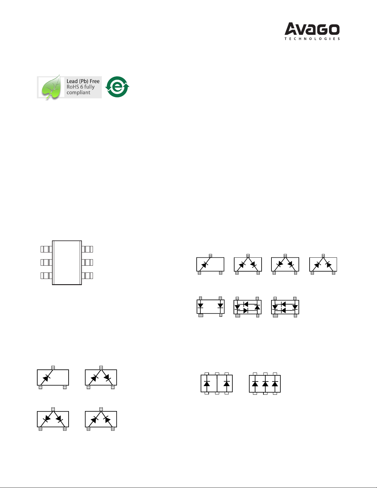
COMMON
CATHODE
#4
UNCONNECTED
PAIR
#5
COMMON
ANODE
#3
SERIES
#2
SINGLE
#0
1 2
3
1 2
3 4
RING
QUAD
#7
1 2
3 4
BRIDGE
QUAD
#8
1 2
3 4
1 2
3
1 2
3
1 2
3
COMMON
CATHODE
F
COMMON
ANODE
E
SERIES
C
SINGLE
B
UNCONNECTED
TRIO
L
1 2 3
6 5 4
HIGH ISOLATION
UNCONNECTED PAIR
K
1 2 3
6 5 4
GUx
1
2
3
6
5
4
Surface Mount RF Schottky Barrier Diodes
Data Sheet
Description/Applications
These Schottky diodes are specically designed for both
analog and digital applications. This series oers a wide
range of specications and package congurations to
give the designer wide exibility. The HSMS‑281x series of
diodes features very low icker (1/f) noise.
Note that Avago’s manufacturing techniques assure that
dice found in pairs and quads are taken from adjacent
sites on the wafer, assuring the highest degree of match.
Pin Connections and Package Marking
Notes:
1.
Package marking provides orientation and identication.
2. See “Electrical Specications” for appropriate package marking.
Features
• Surface Mount Packages
• Low Flicker Noise
• Low FIT (Failure in Time) Rate*
• Six‑sigma Quality Level
• Single, Dual and Quad Versions
• Tape and Reel Options Available
• Lead‑free
• For more information see the Surface Mount Schottky
Reliability Data Sheet.
Package Lead Code Identication, SOT-23/SOT-143
(Top View)
Package Lead Code Identication, SOT-323
(Top View)
Package Lead Code Identication, SOT-363
(Top View)

Absolute Maximum Ratings
[1]
TC = 25°C
Symbol Parameter Unit SOT-23/SOT-143 SOT-323/SOT-363
If Forward Current (1 μs Pulse) Amp 1 1
PIV Peak Inverse Voltage V Same as VBR Same as VBR
Tj Junction Temperature °C 150 150
T
Storage Temperature °C ‑65 to 150 ‑65 to 150
stg
θjc Thermal Resistance
Notes:
1. Operation in excess of any one of these conditions may result in permanent damage to the device.
2. TC = +25°C, where TC is dened to be the temperature at the package pins where contact is made to the circuit board.
ESD WARNING: Handling Precautions Should Be Taken To Avoid Static Discharge.
[2]
°C/W 500 150
Electrical Specications TC = 25°C, Single Diode
[3]
Maximum Maximum
Minimum Maximum Forward Reverse Typical
Part Package Breakdown Forward Voltage Leakage Maximum Dynamic
Number Marking Lead Voltage Voltage VF (V) @ IR (nA) @ Capacitance Resistance
[4]
HSMS
Code Code Conguration VBR (V) VF (mV) IF (mA) VR (V) CT (pF) RD (Ω)
2810 B0 0 Single 20 410 1.0 35 200 15 1.2 15
2812 B2 2 Series
2813 B3 3 Common Anode
2814 B4 4 Common Cathode
2815 B5 5 Unconnected Pair
2817 B7 7 Ring Quad
2818 B8 8 Bridge Quad
[4]
[4]
281B B0 B Single
281C B2 C Series
281E B3 E Common Anode
281F B4 F Common Cathode
281K BK K High Isolation
Unconnected Pair
281L BL L Unconnected Trio
Test Conditions IR = 10 mA IF = 1 mA VF = 0 V IF = 5 mA
f = 1 MHz
Notes:
1. ∆VF for diodes in pairs and quads in 15 mV maximum at 1 mA.
2. ∆CTO for diodes in pairs and quads is 0.2 pF maximum.
3. Eective Carrier Lifetime (τ) for all these diodes is 100 ps maximum measured with Krakauer method at 5 mA.
4. See section titled “Quad Capacitance.”
5. RD = RS + 5.2 Ω at 25°C and If = 5 mA.
[5]
2

Quad Capacitance
C
j
R
j
R
S
Rj =
8.33 X 10⁻⁵ nT
Ib + I
s
where
Ib = externally applied bias current in amps
Is = saturation current (see table of SPICE parameters)
T = temperature, °K
n = ideality factor (see table of SPICE parameters)
Note:
To effectively model the packaged HSMS-281x product,
please refer to Application Note AN1124.
RS = series resistance (see Table of SPICE parameters)
Cj = junction capacitance (see Table of SPICE parameters)
C
1
x C2 C3 x C
4
C
DIAGONAL
= _______ + _______
C
1
+ C2 C3 + C
4
C
1
x C2 C3 x C
4
C
DIAGONAL
= _______ + _______
C
1
+ C2 C3 + C
4
1
C
ADJACENT
= C1 + ____________
1 1 1
–– + –– + ––
C2 C3C
4
Capacitance of Schottky diode quads is measured using
an HP4271 LCR meter. This instrument eectively isolates
individual diode branches from the others, allowing ac‑
curate capacitance measurement of each branch or each
diode. The conditions are: 20 mV R.M.S. voltage at 1 MHz.
Avago denes this measurement as “CM”, and it is equiva‑
lent to the capacitance of the diode by itself. The equiva‑
lent diagonal and adjacent capaci‑tances can then be cal‑
culated by the formulas given below.
In a quad, the diagonal capacitance is the capacitance be‑
tween points A and B as shown in the gure below. The
diagonal capacitance is calculated using the following
formula
The equivalent adjacent capacitance is the capacitance
between points A and C in the gure below. This capaci‑
tance is calculated using the following formula
Linear Equivalent Circuit Model Diode Chip
ESD WARNING:
Handling Precautions Should Be Taken To Avoid Static Discharge.
This information does not apply to cross‑over quad di‑
odes.
3
SPICE Parameters
Parameter Units HSMS-281x
BV V 25
CJ0 pF 1.1
EG eV 0.69
IBV A E‑5
IS A 4.8E‑9
N 1.08
RS Ω 10
PB V 0.65
PT 2
M 0.5
 Loading...