


Distributed by:
Jameco Part Number 1585194
www.Jameco.com ✦ 1-800-831-4242
The content and copyrights of the attached
material are the property of its owner.

GUx
1
2
3
6
5
4
HSMP - 389x & HSMP - 489x Series
Surface Mount RF PIN Switch Diodes
Data Sheet
Description
The HSMP-389x series is optimized for switching applications where low resistance at low current and low
capacitance are required. The HSMP-489x series products
feature ultra low parasitic inductance. These products are
specically designed for use at frequencies which are much
higher than the upper limit for conventional PIN diodes.
Pin Connections and Package Marking
Notes:
1. Package marking provides orientation, identication, and date
code.
2. See “Electrical Specications” for appropriate package marking.
Features
• Unique Congurations in Surface Mount Packages
– Add Flexibility
– Save Board Space
– Reduce Cost
• Switching
– Low Capacitance
– Low Resistance at Low Current
• Low Failure in Time (FIT) Rate
• Matched Diodes for Consistent Performance
• Better Th er mal Conductivity for Higher Power
Dissipation
• Lead-free Option Available
Note:
1. For more information see the Surface Mount PIN Reliability Data Sheet.
[1]

Package Lead Code Identication,
COMMON
CATHODE
#4
COMMON
ANODE
#3
SERIES
#2
SINGLE
#0
UNCONNECTED
PAIR
#5
DUAL ANODE
4890
COMMON
CATHODE
F
COMMON
ANODE
E
SERIES
C
SINGLE
B
DUAL ANODE
489B
SERIESÐ
SHUNT PAIR
LOW
INDUCTANCE
SINGLE
T
UNCONNECTED
TRIO
L
1 2 3
6 5 4
1 2 3
6 5 4
1 2 3
6 5 4
U
HIGH
FREQUENCY
SERIES
V
1 2 3
6 5 4
DUAL SWITCH
MODEL
R
1 2 3
6 5 4
SOT-23/143 (Top View)
Package Lead Code Identication,
SOT-323 (Top View)
Package Lead Code Identication,
SOT-363 (Top View)
ESD WARNING:
Handling Precautions Should Be Taken To Avoid Static Discharge.
Absolute Maximum Ratings
[1]
TC = +25°C
Symbol Parameter Unit SOT-23/143 SOT-323/363
If Forward Current (1 µs Pulse) Amp 1 1
P
IV
T
j
T
stg
θ
jc
Notes:
1. Operation in excess of any one of these conditions may result in permanent damage to the device.
2. TC = +25°C, where TC is dened to be the temperature at the package pins where contact is made to the circuit board.
Peak Inverse Voltage V 100 100
Junction Temperature °C 150 150
Storage Temperature °C -65 to 150 -65 to 150
Thermal Resistance
[2]
°C/W 500 150
2

Electrical Specications, TC = 25°C, each diode
Part Number
HSMP-
3890
3892
3893
3894
3895
389B
389C
389E
389F
389L
389R
389T
389U
389V
Package
Marking
Code
G0
G2
G3
G4
G5
G0
G2
G3
G4
GL
S
Z
GU
GV
Lead
Code
0
2
3
4
5
B
C
E
F
L
R
T
U
V
Conguration Minimum
Breakdown
Voltage VBR (V)
Single
100 2.5 0.30
Series
Common Anode
Common Cathode
Unconnected Pair
Single
Series
Common Anode
Common Cathode
Unconnected Trio
Dual Switch Mode
Low Inductance
Single
Series-Shunt Pair
High Frequency
Series Pair
Test Conditions VR = V
Measure
IR ≤ 10 µA
BR
Maximum
Series Resistance
RS (Ω)
IF = 5 mA
f = 100 MHz
Maximum
Total Capacitance
CT (pF)
VR = 5 V
f = 1 MHz
High Frequency (Low Inductance, 500 MHz–3 GHz) PIN Diodes
Part
Number
HSMP-
489x GA Dual Anode 100 2.5 0.33 0.375 1.0
Test Conditions
Package
Marking
[1]
Code
Conguration Minimum
Breakdown
Voltage
VBR (V)
VR = V
BR
Measure
IR ≤ 10 µA
Maximum
Series
Resistance
RS (Ω)
Typical
Total
Capacitance
CT (pF)
IF = 5 mA f = 1 MHz
VR = 5 V
Maximum
Total
Capacitance
CT (pF)
VR = 5 V
f = 1 MHz
Typical Parameters at TC = 25°C
Part Number
HSMP-
389x 3.8 200 0.20 @ 5V
Test Conditions
Series Resistance
IF = 1 mA
f = 100 MHz
RS (Ω)
Carrier Lifetime
IF = 10 mA
IR = 6 mA
τ
(ns)
Total Capacitance
CT (pF)
Typical
Total
Inductance
LT (nH)
f=500 MHz–
3 GHz
3
HSMP-389x Series Typical Performance, TC = 25°C, each diode
1
123
405 6
b1 b2 b3
2
3
1
1 1
RF in
RF out
2
2
3
4 5 6
1
0
0
2
+V
-V
"ON"
"OFF"
Figure 1. Total RF Resistance at 25 C
vs. Forward Bias Current.
100
10
1
0.1
RF RESISTANCE (OHMS)
IF - FORWARD BIAS CURRENT (mA)
0.01 0.1 1 10 100
200
160
120
80
40
0
10 2015 25 30
T
rr
- REVERSE RECOVERY TIME (nS)
FORWARD CURRENT (mA)
Figure 4. Typical Reverse Recovery
Time vs. Reverse Voltage.
VR = - 2V
VR = - 5V
VR = - 10 V
0.55
0.50
0.45
0.40
0.35
0.30
0.25
0.20
04 8 1 2 16 2 0
V
R
- REVERSE VOLTAGE (V)
TOTAL CAPACITANCE (pF)
1 MHz
1 GHz
Figure 2. Capacitance vs. Reverse
Voltage.
100
10
1
0.1
0.01
0 0.2 0.4 0.6 0.8 1.0 1.2
I
F
- FORWARD CURRENT (mA)
VF - FORWARD VOLTAGE (V)
Figure 5. Forward Current vs. Forward
Voltage.
125˚ C
25˚C
- 50˚C
120
115
110
105
100
95
90
85
11 0 30
IF - FORWARD BIAS CURRENT (mA)
Figure 3. 2nd Harmonic Input Intercept
Point vs. Forward Bias Current.
INPUT INTERCEPT POINT (dBm)
Diode Mounted as a
Series Attenuator in a
50 Ohm Microstrip and
Tested at 123 MHz
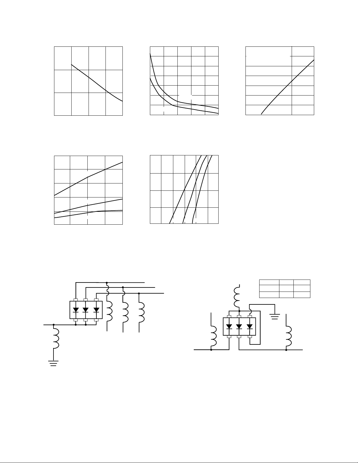
Typical Applications for Multiple Diode Products
Figure 6. HSMP-389L used in a SP3T Switch. Figure 7. HSMP-389L Unconnected Trio used in a Dual Volt-
4
age, High Isolation Switch.

Typical Applications for Multiple Diode Products (continued)
4
Rcvr
Xmtr
Bias
Ant
PA
bias
HSMP-389U
LNA
4
Rcvr
Bias
Xmtr
HSMP-389V
Antenna
4
4
Rcvr
Xmtr
Bias
Ant
C C
λ
λ
λ
λ
RF in
RF out
1
+V
0
2
0
+V
"ON"
"OFF"
456
11223
RF in
RF out
456
12 3
1
Figure 8. HSMP-389L Unconnected Trio used in a Positive
Voltage, High Isolation Switch.
Figure 10. HSMP-389U Series/Shunt Pair used in a 900 MHz
Transmit/Receive Switch.
Figure 9. HSMP-389T used in a Low Inductance Shunt
Mounted Switch.
Figure 11. HSMP-389V Series/Shunt Pair used in a 1.8 GHz
Transmit/Receive Switch.
5

Typical Applications for Multiple Diode Products (continued)
RF COMMON
RF COMMON
RF 1
BIAS 1
BIAS BIAS
RF 2
BIAS 2
Figure 12. Simple SPDT Switch, Using Only Positive Current. Figure 13. High Isolation SPDT Switch, Dual Bias.
RF 2
RF 1
RF COMMON
RF 1 RF 2
BIAS
Figure 14. Switch Using Both Positive and Negative Bias
Current.
Figure 15. Very High Isolation SPDT Switch, Dual Bias.
RF COMMON
RF 2
RF 1
BIAS
6

1 2
3
HSMP-489x
0.12 pF*
* Measured at -20 V
0.5 Ω
R
j
R
s
C
j
Rj =
20
Ω
I
0.9
RT = 0.5 + R
j
I = Forward Bias Current in mA
* See AN1124 for package models
50 OHM MICROSTRIP LINES
PAD CONNECTED TO
GROUND BY TWO
VIA HOLES
0.3 nH
0.3 nH
0.3 pF
1.5 nH 1.5 nH
CT = CP + R
j
Co-Planar Waveguide
Groundplane
Center Conductor
Groundplane
0.3 pF
0.75 nH
Typical Applications for HSMP-489x Low Inductance Series
Microstrip Series Connection for HSMP-489x Series
In order to take full advantage of the low inductance of the
HSMP-489x series when using them in series applications,
both lead 1 and lead 2 should be connected together, as
shown in Figure 17.
Figure 16. Internal Connections.
Figure 17. Circuit Layout.
Figure 18. Circuit Layout.
Microstrip Shunt Connections for HSMP-489x Series
In Figure 18, the center conductor of the microstrip line is
interrupted and leads 1 and 2 of the HSMP-489x diode are
placed across the resulting gap. This forces the 1.5 nH lead
inductance of leads 1 and 2 to appear as part of a low pass
lter, reducing the shunt parasitic inductance and increasing the maximum available attenuation. The 0.3 nH of shunt
inductance external to the diode is created by the via holes,
and is a good estimate for 0.032” thick material.
Co-Planar Waveguide Shunt Connection for HSMP-489x Series
Co-Planar waveguide, with ground on the top side of
the printed circuit board, is shown in Figure 20. Since it
eliminates the need for via holes to ground, it oers lower
shunt parasitic inductance and higher maximum attenuation when compared to a microstrip circuit.
Figure 20. Circuit Layout.
Figure 19. Equivalent Circuit.
Equivalent Circuit Model: HSMP-389x Chip*
Figure 21. Equivalent Circuit.
7
A SPICE model is not available for PIN diodes as SPICE
does not provide for a key PIN diode characteristic, carrier lifetime.

Assembly Information
DIMENSIONS IN
inches
mm
0.061
2.05 0.071
1.8
0.112
2.85
0.079
2
0.033
0.85
0.048
1.2
0.114
2.9
0.033
0.85
0.047
1.2
0.031
0.8
0.033
0.85
0.039
1
0.039
1
0.079
2.0
0.031
0.8
DIMENSIONS IN
inches
mm
0.035
0.9
0.026
0.079
0.018
0.039
0.026
0.039
0.079
0.022
TIME (seconds)
T
MAX
TEMPERATURE (˚C)
0
0
50
100
150
200
250
60
Preheat
Zone
Cool Down
Zone
Reflow
Zone
120 180 240 300
Figure 22. Recommended PCB Pad Layout for Avago Technologies’
SC70 6L / SOT-363 Products.
Figure 23. Recommended PCB Pad Layout for Avago Technologies’
SC70 3L / SOT-323 Products.
SMT Assembly
Reliable assembly of surface mount components is a
complex process that involves many material, process, and
equipment factors, including: method of heating (e.g., IR
or vapor phase reow, wave soldering, etc.) circuit board
material, conductor thickness and pattern, type of solder
alloy, and the thermal conductivity and thermal mass of
components. Components with a low mass, such as the
SOT package, will reach solder reow temperatures faster
than those with a greater mass.
Avago Technologies’ diodes have been qualied to the
time-temperature prole shown in Figure 26. This prole
is representative of an IR reow type of surface mount
assembly process.
After ramping up from room temperature, the circuit
board with components attached to it (held in place with
solder paste) passes through one or more preheat zones.
The preheat zones increase the temperature of the board
and components to prevent thermal shock and begin
evaporating solvents from the solder paste. The reow zone
briey elevates the temperature suciently to produce a
reow of the solder.
The rates of change of temperature for the ramp-up and
cool-down zones are chosen to be low enough to not cause
deformation of the board or damage to components due
to thermal shock. The maximum temperature in the reow
zone (T
These parameters are typical for a surface mount assembly process for Avago Technologies diodes. As a general
guideline, the circuit board and components should be
exposed only to the minimum temperatures and times
necessary to achieve a uniform reow of solder.
) should not exceed 235°C.
MAX
Figure 24. Recommended PCB Pad Layout for Avago Technologies’
SOT-23 Products.
Figure 25. Recommended PCB Pad Layout for Avago Technologies’
SOT-143 Products.
8
Figure 26. Surface Mount Assembly Prole.

Package Dimensions
XXX
E
E1
D
A
A1
B
e1
e
L
C
MIN MAX
A 0.8 1
A1 0 0.1
B 0.15 0.4
C 0.1 0.2
D
1.8 2.25
E1 1.1 1.4
e
e1
E 1.8 2.4
L
0.425 typical
SYMBOL
AGILENT
0.65 typical
1.30 typical
MIN
(mm)
MAX
(mm)
E 1.15 1.35
D 1.8 2.25
HE 1.8 2.4
A 0.8 1.1
A2 0.8 1
A1 0 0.1
Q1 0.1 0.4
e
b 0.15 0.3
c 0.1 0.2
L 0.1 0.3
Symbol
Agilent (New)
0.650 BCS
Outline SOT-363 (SC-70 6 Lead)
Outline SOT-323 (SC-70 3 Lead)
9

XXX
E
E1
D
A
A1
B
e1
e
L
C
SYMBOL MIN MAX
A 0.79 1.097
A1 0.013 0.1
B 0.36 0.54
B1 0.76 0.92
C 0.086 0.152
D 2.8 3.06
E1 1.2 1.4
e 0.89 1.02
e1 1.78 2.04
e2 0.45 0.6
E 2.1 2.65
L 0.45 0.69
AGILENT
XXX
E
E1
D
A
A1
B
e1
e
C
e2
MIN MAX
A 0.79 1.2
A1 0 0.1
B 0.37 0.54
C 0.086 0.152
D
2.73 3.13
E1 1.15 1.5
e 0.89 1.02
e1 1.78 2.04
e2 0.45 0.6
E 2.1 2.7
L 0.45 0.69
SYMBOL
AGILENT
Outline 23 (SOT-23)
Outline 143 (SOT-143)
10

Device Orientation
USER
FEED
DIRECTION
COVER TAPE
CARRIER
TAPE
REEL
Note: "AB" represents package marking code.
"C" represents date code.
END VIE
W
8 mm
4 mm
TOP VIEW
ABCABCABCABC
Note: "AB" represents package marking code.
"C" represents date code.
END VIE
W
8 mm
4 mm
TOP VIEW
ABC ABC ABC ABC
END VIE
W
8 mm
4 mm
TOP VIEW
Note: "AB" represents package marking code.
"C" represents date code.
ABC ABC ABC ABC
9 MAX
A
0
P
P
0
D
P
2
E
F
W
D
1
Ko
8 MAX
B
0
13.5 MAX
t1
DESCRIPTION SYMBOL SIZE (mm) SIZE (INCHES)
LENGTH
WIDTH
DEPTH
PITCH
BOTTOM HOLE DIAMETER
A
0
B
0
K
0
P
D
1
3.15 ± 0.10
2.77 ± 0.10
1.22 ± 0.10
4.00 ± 0.10
1.00 + 0.05
0.124 ± 0.004
0.109 ± 0.004
0.048 ± 0.004
0.157 ± 0.004
0.039 ± 0.002
CAVITY
DIAMETER
PITCH
POSITION
D
P
0
E
1.50 + 0.10
4.00 ± 0.10
1.75 ± 0.10
0.059 + 0.004
0.157 ± 0.004
0.069 ± 0.004
PERFORATION
WIDTH
THICKNESS
Wt18.00 + 0.30 – 0.10
0.229 ± 0.013
0.315 + 0.012 – 0.004
0.009 ± 0.0005
CARRIER TAPE
CAVITY TO PERFORATION
(WIDTH DIRECTION)
CAVITY TO PERFORATION
(LENGTH DIRECTION)
F
P
2
3.50 0.05
2.00 ± 0.05
0.138 ± 0.002
0.079 ± 0.002
DISTANCE
BETWEEN
CENTERLINE
For Outlines SOT-23, -323
For Outline SOT-143
Tape Dimensions and Product Orientation
For Outline SOT-23
For Outline SOT-363
11

Tape Dimensions and Product Orientation
W
F
E
P
2
P
0
D
P
D
1
DESCRIPTION SYMBOL SIZE (mm) SIZE (INCHES)
LENGTH
WIDTH
DEPTH
PITCH
BOTTOM HOLE DIAMETER
A
0
B
0
K
0
P
D
1
3.19 ± 0.10
2.80 ± 0.10
1.31 ± 0.10
4.00 ± 0.10
1.00 + 0.25
0.126 ± 0.004
0.110 ± 0.004
0.052 ± 0.004
0.157 ± 0.004
0.039 + 0.010
CAVITY
DIAMETER
PITCH
POSITION
D
P
0
E
1.50 + 0.10
4.00 ± 0.10
1.75 ± 0.10
0.059 + 0.004
0.157 ± 0.004
0.069 ± 0.004
PERFORATION
WIDTH
THICKNESS
Wt18.00 + 0.30 – 0.10
0.254 ± 0.013
0.315+ 0.012 – 0.004
0.0100 ± � 0.0005
CARRIER TAPE
CAVITY TO PERFORATION
(WIDTH DIRECTION)
CAVITY TO PERFORATION
(LENGTH DIRECTION)
F
P
2
3.50 ± 0.05
2.00 ± 0.05
0.138 ± 0.002
0.079 ± 0.002
DISTANCE
A
0
9˚� MAX 9˚� MAX
t
1
B
0
K
0
P
P
0
P
2
F
W
C
D
1
D
E
A
0
An
t1 (CARRIER TAPE THICKNESS) Tt (COVER TAPE THICKNESS)
An
B
0
K
0
DESCRIPTION SYMBOL SIZE (mm) SIZE (INCHES)
LENGTH
WIDTH
DEPTH
PITCH
BOTTOM HOLE DIAMETER
A
0
B
0
K
0
P
D
1
2.40 ± 0.10
2.40 ± 0.10
1.20 ± 0.10
4.00 ± 0.10
1.00 + 0.25
0.094 ± 0.004
0.094 ± 0.004
0.047 ± 0.004
0.157 ± 0.004
0.039 + 0.010
CAVITY
DIAMETER
PITCH
POSITION
D
P
0
E
1.55 ± 0.05
4.00 ± 0.10
1.75 ± 0.10
0.061 ± 0.002
0.157 ± 0.004
0.069 ± 0.004
PERFORATION
WIDTH
THICKNESS
W
t
1
8.00 ± 0.30
0.254 ± 0.02
0.315 ± 0.012
0.0100 ± 0.0008
CARRIER TAPE
CAVITY TO PERFORATION
(WIDTH DIRECTION)
CAVITY TO PERFORATION
(LENGTH DIRECTION)
F
P
2
3.50 ± 0.05
2.00 ± 0.05
0.138 ± 0.002
0.079 ± 0.002
DISTANCE
FOR SOT-323 (SC70-3 LEAD) An 8°�C MAX
FOR SOT-363 (SC70-6 LEAD) 10°�C MAX
ANGLE
WIDTH
TAPE THICKNESS
C
T
t
5.4 ± 0.10
0.062 ± 0.001
0.205 ± 0.004
0.0025 ± 0.00004
COVER TAPE
For Outline SOT-143
For Outlines SOT-323, -363
12

Ordering Information
Specify part number followed by option. For example:
HSMP - 389x - XXX
Bulk or Tape and Reel Option
Part Number; x = Lead Code
Surface Mount PIN
Option Descriptions
-BLK = Bulk, 100 pcs. per antistatic bag
-TR1 = Tape and Reel, 3000 devices per 7” reel
-TR2 = Tape and Reel, 10,000 devices per 13” reel
Tape and Reeling conforms to Electronic Industries RS-481, “Taping of Surface Mounted Components for Automated
Placement.”
For lead-free option, the part number will have the character “G” at the end, eg. -TR2G for a 10K pc lead-free reel.
Package Characteristics
Lead Material ..................................Copper (SOT-323/363); Alloy 42 (SOT-23/143)
Lead Finish ................................................. Tin-Lead 85-15% (Non lead-free option)
................................................................................................Tin 100% (Lead-free option)
Maximum Soldering Temperature ............................................ 260°C for 5 seconds
Minimum Lead Strength ........................................................................... 2 pounds pull
Typical Package Inductance ...................................................................................... 2 nH
Typical Package Capacitance ..............................................0.08 pF (opposite leads)
For product information and a complete list of distributors, please go to our web site: www.avagotech.com
Avago, Avago Technologies, and the A logo are trademarks of Avago Technologies, Pte. in the United States and other countries.
Data subject to change. Copyright © 2006 Avago Technologies Pte. All rights reserved.
5989-3860EN - March 29, 2006
13
 Loading...