

HLMP-HG65, HLMP-HM65, HLMP-HB65
Precision Optical Performance Red Green and Blue
New 5mm Standard Oval LEDs
Data Sheet
Description
These Precision Optical Performance Oval LEDs are speci cally designed for full color/video and passenger information signs. The oval shaped radiation pattern and
high luminous intensity ensure that these devices are
excellent for wide eld of view outdoor applications
where a wide viewing angle and readability in sunlight
are essential. The package epoxy contains both UV-A
and UV-B inhibitors to reduce the e ects of long term
exposure to direct sunlight.
Applications
• Full color signs
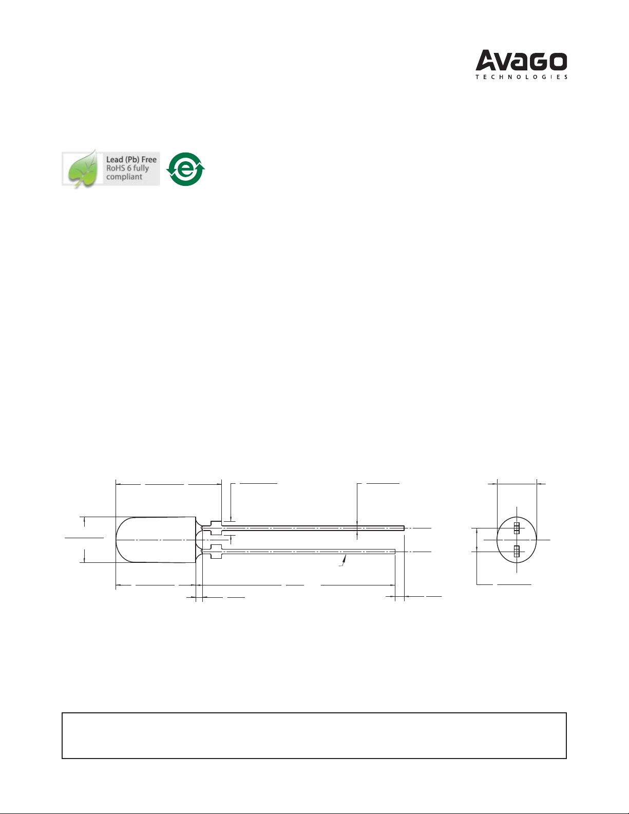
Package Dimensions
10.80 ± 0.50
0.425 ± 0.020
5.20 ± 0.20
0.205 ± 0.008
1.30 ± 0.20
0.051 ± 0.008
Features
• Well de ned spatial radiation pattern
• High brightness material
• Available in Red, Green and Blue color
Red AlInGaP 626 nm
Green InGaN 525nm
Blue InGaN 470nm
• Superior resistance to moisture
• Stando Package
• Tinted and di used
• Typical viewing angle 40° x 100°
MEASURED AT BASE OF LENS.
0.50 ± 0.10
0.020 ± 0.004
sq. typ.
3.80 ± 0.20
0.150 ± 0.008
7.00 ± 0.20
0.276 ± 0.008
Notes:
All dimensions in millimeters (inches).
CAUTION: INGaN devices are Class 1C HBM ESD sensitive per JEDEC Standard. Please observe appropriate
precautions during handling and processing. Refer to Application Note AN – 1142 for additional details.
1.02
0.040
max.
cathode lead
24.00
0.945
min.
1.00
0.039
min.
2.54 ± 0.30
0.10 ± 0.012
Device Selection Guide
Color and Dominant Wavelength
Part Number
HLMP-HG65-VY0xx Red 626 1150 2400
HLMP-HM65-Y30xx Green 525 1990 5040
HLMP-HB65-QU0xx Blue 470 460 1150
Tolerance for each intensity limit is ± 15%.
Notes:
1. The luminous intensity is measured on the mechanical axis of the lamp package and it is tested in pulsing condition.
λd (nm) Typ
Luminous Intensity Iv
(mcd) at 20 mA-Min
[1]
Luminous Intensity Iv
(mcd) at 20 mA-Max
Part Numbering System
HLMP-H x 65 - x x x xx
Packaging Option
ZZ: Flexi Ammopack
DD: Ammopacks
Color Bin Selection
0: Open distribution
[1]
Maximum Intensity Bin
0: No maximum intensity limit
Minimum Intensity Bin
Refer to Device Selection Guide.
Standoff/Non Standoff
5: Standoff
Color
G: Red 626
M: Green 525
B: Blue 470
Package
H: 5mm Standard Oval 40° x 100°
Note:
Please refer to AB 5337 for complete information about part numbering system.
2
Absolute Maximum Ratings
TJ = 25°C
Parameter Red Green and Blue Unit
DC Forward Current
Peak Forward Current 100
Power Dissipation 120 116 mW
Reverse Voltage 5 (I
LED Junction Temperature 130 110 °C
Operating Temperature Range -40 to +100 -40 to +85 °C
Storage Temperature Range -40 to +100 -40 to +100 °C
Notes:
1. Derate linearly as shown in Figure 4.
2. Duty Factor 30%, frequency 1KHz.
3. Duty Factor 10%, frequency 1KHz.
[1]
50 30 mA
[2]
= 100 μA) 5 (IR = 10 μA) V
R
100
[3]
Electrical / Optical Characteristics
TJ = 25°C
Parameter Symbol Min. Typ. Max. Units Test Conditions
Forward Voltage
Red
Green
Blue
Reverse Voltage
Red
Green & blue
Dominant Wavelength
Red
Green
Blue
Peak Wavelength
Red
Green
Blue
Thermal Resistance
Luminous E cacy
[2]
Red
Green
Blue
[1]
V
V
λ
λ
Rθ
η
F
R
d
PEAK
J-PIN
V
1.8
2.8
2.8
5
5
618
520
460
2.1
3.2
3.2
VI
2.4
3.8
3.8
= 20 mA
F
V
IF = 100 μA
IF = 10 μA
nm IF = 20 mA
626
525
470
634
516
630
540
480
nm Peak of Wavelength of Spectral
Distribution at IF = 20 mA
464
240 °C/W LED Junction-to-Pin
150
530
lm/W Emitted Luminous Power/Emitted
Radiant Power
65
mA
Notes:
1. The dominant wavelength is derived from the chromaticity Diagram and represents the color of the lamp
2. The radiant intensity, Ie in watts per steradian, may be found from the equation Ie = IV/ηV where IV is the luminous intensity in candelas and ηV is
the luminous e cacy in lumens/watt.
3
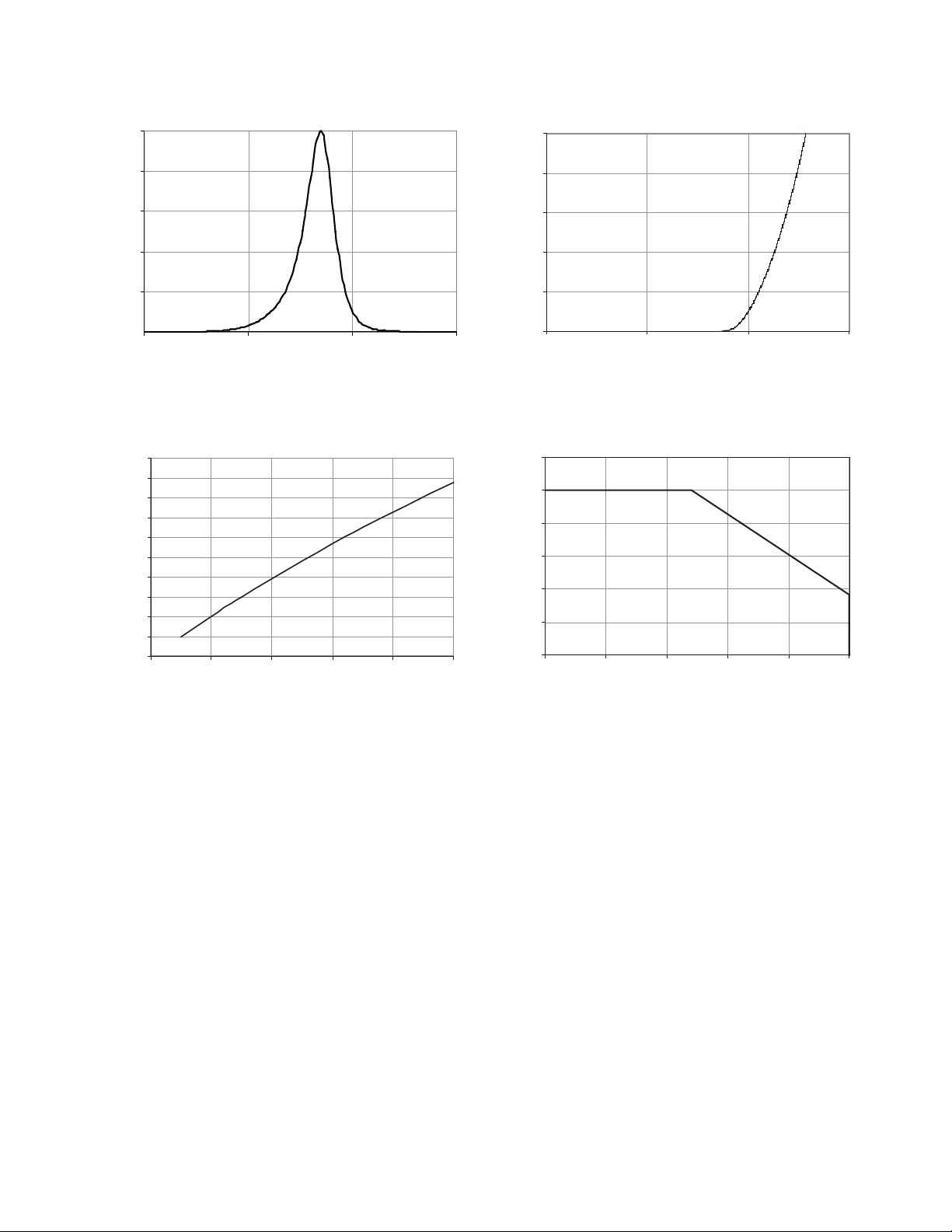
AlInGaP Red
1
0.8
0.6
0.4
RELATIVE INTENSITY
0.2
0
550 600 650 700
WAVELENGTH - nm
Figure 1. Relative Intensity vs Wavelength
5.0
4.5
4.0
3.5
3.0
2.5
2.0
1.5
(NORMALIZED AT 20 mA)
1.0
RELATIVE LUMINOUS INTENSITY
0.5
0.0
0 20406080100
DC FORWARD CURRENT - mA
100
80
60
40
FORWARD CURRENT - mA
20
0
0123
FORWARD VOLTAGE - V
Figure 2. Forward Current vs Forward Voltage
60
50
40
30
20
10
- MAXIMUM FORWARD CURRENT - mA
.
F MAX
0
I
0 20 40 60 80 100
T
- AMBIENT TEMPERATURE - C
A
Figure 3. Relative Intensity vs Forward Current Figure 4. Maximum Forward Current vs Ambient Temperature
4

InGaN Blue and Green
1.0
100
0.9
0.8
0.7
0.6
GREENBLUE
80
60
0.5
0.4
RELATIVE INTENSITY
0.3
0.2
40
FORWARD CURRENT - mA
20
0.1
0.0
380 430 480 530 580 630
WAVELENGTH - nm
0
012345
FORWARD VOLTAGE - V
Figure 5. Relative Intensity vs Wavelength Figure 6. Forward Current vs Forward Voltage
3.5
3.0
2.5
2.0
1.5
BLUE
GREEN
35
30
25
CURRENT - mA
20
15
1.0
(NORMALIZED AT 20mA)
RELATIVE LUMINOUS INTENSITY
0.5
0.0
0 20 40 60 80 100 120
DC FORWARD CURRENT - mA
10
5
max - MAXIMUM FORWARD
F
0
I
0 20 40 60 80 100
T
- AMBIENT TEMPERATURE - °C
A
Figure 7. Relative Intensity vs Forward Current Figure 8. Maximum Forward Current vs Ambient Temperature
10
8
6
4
2
0
-2
-4
-6
-8
-10
RELATIVE DOMINANT WAVELENGTH SHIFT -nm
0 20 40 60 80 100
FORWARD CURRENT-mA
BLUE
GREEN
Figure 9. Relative dominant wavelength vs Forward Current
5

1.0
0.9
0.8
RED
BLUE
GREEN
0.7
0.6
0.5
0.4
0.3
NORMALIZED INTENSITY
0.2
0.1
0.0
-90 -60 -30 0 30 60 90
ANGULAR DISPLACEMENT - DEGREES
Figure 10. Radiation Pattern – Major Axis Figure 11. Radiation Pattern – Minor Axis
1.0
0.9
0.8
0.7
0.6
0.5
0.4
0.3
NORMALIZED INTENSITY
0.2
0.1
0.0
-90 -60 -30 0 30 60 90
ANGULAR DISPLACEMENT - DEGREES
RED
BLUE
GREEN
10
1
RELATIVE LIGHT OUTPUT
(NORMALIZED AT TJ = 25°C)
0.1
-40 -20 0 20 40 60 80 100 120 140
TJ - JUNCTION TEMPERATURE - °C
Figure12. Relative Light Output vs Junction Temperature Figure 13. Relative Forward Voltage vs Junction Temperature
RED
GREEN
BLUE
0.3
0.2
0.1
0
-0.1
-0.2
FORWARD VOLTAGE SHIFT-V
-0.3
-0.4
-40 -20 0 20 40 60 80 100 120 140
TJ -JUNCTION TEMPERATURE
RED
GREEN
BLUE
6

Intensity Bin Limit Table (1.2: 1 Iv Bin Ratio)
Green Color Bin Table
Intensity (mcd) at 20 mA
Bin
Q 460 550
R 550 660
S 660 800
T 800 960
U 960 1150
V 1150 1380
W 1380 1660
X 1660 1990
Y 1990 2400
Z 2400 2900
1 2900 3500
2 3500 4200
3 4200 5040
Tolerance for each bin limit is ± 15%
Min Max
VF Bin Table (V at 20mA)
Bin ID Min Max
VD 1.8 2.0
VA 2.0 2.2
VB 2.2 2.4
Notes:
1. Tolerance for each bin limit is ±0.05V
2. VF binning only applicable to Red color.
Red Color Range
Min
Dom
618 630 0.6872 0.3126 0.6890 0.2943
Max
Dom Xmin Ymin Xmax Ymax
0.6690 0.3149 0.7080 0.2920
Min
Bin
Dom
1 520.0 524.0 0.0743 0.8338 0.1856 0.6556
2 524.0 528.0 0.1060 0.8292 0.2068 0.6463
3 528.0 532.0 0.1387 0.8148 0.2273 0.6344
4 532.0 536.0 0.1702 0.7965 0.2469 0.6213
5 536.0 540.0 0.2003 0.7764 0.2659 0.6070
Tolerance for each bin limit is ± 0.5nm.
Max
Dom Xmin Ymin Xmax Ymax
0.1650 0.6586 0.1060 0.8292
0.1856 0.6556 0.1387 0.8148
0.2068 0.6463 0.1702 0.7965
0.2273 0.6344 0.2003 0.7764
0.2469 0.6213 0.2296 0.7543
Blue Color Bin Table
Min
Bin
Dom
1 460.0 464.0 0.1440 0.0297 0.1766 0.0966
2 464.0 468.0 0.1374 0.0374 0.1699 0.1062
3 468.0 472.0 0.1291 0.0495 0.1616 0.1209
4 472.0 476.0 0.1187 0.0671 0.1517 0.1423
5 476.0 480.0 0.1063 0.0945 0.1397 0.1728
Tolerance for each bin limit is ± 0.5nm
Note:
1. All bin categories are established for classi cation of products.
Products may not be available in all bin categories. Please contact
your Avago representative for further information.
Max
Dom Xmin Ymin Xmax Ymax
0.1818 0.0904 0.1374 0.0374
0.1766 0.0966 0.1291 0.0495
0.1699 0.1062 0.1187 0.0671
0.1616 0.1209 0.1063 0.0945
0.1517 0.1423 0.0913 0.1327
Tolerance for each bin limit is ± 0.5nm
7

Avago Color Bin on CIE 1931 Chromaticity Diagram
1.000
0.800
Green
0.600
Y
0.400
0.200
0.000
0.000 0.100 0.200 0.300 0.400 0.500 0.600 0.700 0.800
1
2
3
4
5
Red
Blue
5
4
3
2
1
X
8

Precautions:
Lead Forming:
• The leads of an LED lamp may be preformed or cut to
length prior to insertion and soldering on PC board.
• For better control, it is recommended to use proper
tool to precisely form and cut the leads to applicable
length rather than doing it manually.
• If manual lead cutting is necessary, cut the leads after
the soldering process. The solder connection forms a
mechanical ground which prevents mechanical stress
due to lead cutting from traveling into LED package.
This is highly recommended for hand solder operation,
as the excess lead length also acts as small heat sink.
Soldering and Handling:
• Care must be taken during PCB assembly and
soldering process to prevent damage to the LED
component.
• LED component may be e ectively hand soldered
to PCB. However, it is only recommended under
unavoidable circumstances such as rework. The closest
manual soldering distance of the soldering heat
source (soldering iron’s tip) to the body is 1.59mm.
Soldering the LED using soldering iron tip closer than
1.59mm might damage the LED.
1.59mm
• ESD precaution must be properly applied on the
soldering station and personnel to prevent ESD
damage to the LED component that is ESD sensitive.
Do refer to Avago application note AN 1142 for details.
The soldering iron used should have grounded tip to
ensure electrostatic charge is properly grounded.
• Recommended soldering condition:
Wave
Soldering
Pre-heat temperature 105 °C Max. -
Preheat time 60 sec Max -
Peak temperature 260 °C Max. 260 °C Max.
Dwell time 5 sec Max. 5 sec Max
Note:
1. Above conditions refers to measurement with thermocouple
mounted at the bottom of PCB.
2. It is recommended to use only bottom preheaters in order to
reduce thermal stress experienced by LED.
[1, 2]
• Wave soldering parameters must be set and
maintained according to the recommended
temperature and dwell time. Customer is advised
to perform daily check on the soldering pro le to
ensure that it is always conforming to recommended
soldering conditions.
Manual Solder
Dipping
Note:
1. PCB with di erent size and design (component density) will have
di erent heat mass (heat capacity). This might cause a change in
temperature experienced by the board if same wave soldering
setting is used. So, it is recommended to re-calibrate the soldering
pro le again before loading a new type of PCB.
2. Avago Technologies’ AllnGaP high brightness LED are using high
e ciency LED die with single wire bond as shown below. Customer
is advised to take extra precaution during wave soldering to ensure
that the maximum wave temperature does not exceed 260°C and
the solder contact time does not exceeding 5sec. Over-stressing the
LED during soldering process might cause premature failure to the
LED due to delamination.
Avago Technologies LED con guration
CATHODE
InGaN Device
• Any alignment xture that is being applied during
wave soldering should be loosely tted and should
not apply weight or force on LED. Non metal material
is recommended as it will absorb less heat during
wave soldering process.
• At elevated temperature, LED is more susceptible to
mechanical stress. Therefore, PCB must allowed to cool
down to room temperature prior to handling, which
includes removal of alignment xture or pallet.
• If PCB board contains both through hole (TH) LED and
other surface mount components, it is recommended
that surface mount components be soldered on the
top side of the PCB. If surface mount need to be on the
bottom side, these components should be soldered
using re ow soldering prior to insertion the TH LED.
• Recommended PC board plated through holes (PTH)
size for LED component leads.
LED component
lead size Diagonal
0.45 x 0.45 mm
(0.018x 0.018 inch)
0.50 x 0.50 mm
(0.020x 0.020 inch)
• Over-sizing the PTH can lead to twisted LED after
clinching. On the other hand under sizing the PTH can
cause di culty inserting the TH LED.
Refer to application note AN5334 for more information about
soldering and handling of high brightness TH LED lamps.
ANDOE
AlInGaP Device
0.636 mm
(0.025 inch)
0.707 mm
(0.028 inch)
Plated through
hole diameter
0.98 to 1.08 mm
(0.039 to 0.043 inch)
1.05 to 1.15 mm
(0.041 to 0.045 inch)
9

Example of Wave Soldering Temperature Pro le for TH LED
260°C Max
105°C Max
Recommended solder:
Sn63 (Leaded solder alloy)
SAC305 (Lead free solder alloy)
Flux: Rosin flux
Solder bath temperature: 255°C ± 5°C
(maximum peak temperature = 260°C)
TEMPERATURE (°C)
Ammo Packs Drawing
6.35±1.30
0.25±0.0512
60 sec Max
Dwell time: 3.0 sec - 5.0 sec
(maximum = 5sec)
Note: Allow for board to be sufficiently
cooled to room temperature before
exerting mechanical force.
TIME (sec)
12.70±1.00
0.50±0.0394
CATHODE
9.125±0.625
0.3593±0.0246
18.00±0.50
0.7087±0.0197
12.70±0.30
0.50±0.0118
Note: All dimensions in millimeters (inches)
10
0.70±0.20
0.0276±0.0079
A
VIEW A - A
20.50±1.00
0.8071±0.0394
4.00±0.20
Ø
A
0.1575±0.008
TYP

Packaging Box for Ammo Packs
FROM LEFT SIDE OF BOX
ADHESIVE TAPE MUST BE
FACING UPWARDS.
ANODE LEAD LEAVES
THE BOX FIRST.
LABEL ON THIS
SIDE OF BOX
Note: For InGaN device, the ammo pack packaging box contain ESD logo
Packaging Label
(i) Avago Mother Label: (Available on packaging box of ammo pack and shipping box)
(1P) Item: Part Number
(1T) Lot: Lot Number
LPN:
(9D)MFG Date: Manufacturing Date
(P) Customer Item:
(V) Vendor ID:
(9D) Date Code: Date Code
DeptID: Made In: Country of Origin
STANDARD LABEL LS0002
RoHS Compliant
e3 max temp 260C
(Q) QTY: Quantity
CAT: Intensity Bin
BIN: Refer to below information
11

(ii) Avago Baby Label (Only available on bulk packaging)
p
Lamps Baby Label
RoHS Compliant
e3 max tem
(1P) PART #: Part Number
(1T) LOT #: Lot Number
260C
(9D)MFG DATE: Manufacturing Date
C/O: Country of Origin
Customer P/N:
Supplier Code:
QUANTITY: Packing Quantity
CAT: Intensity Bin
BIN: Refer to below information
DATECODE: Date Code
Acronyms and De nition:
BIN:
(i) Color bin only or VF bin only
(Applicable for part number with color bins but
without VF bin OR part number with VF bins and no
color bin)
OR
(ii) Color bin incorporated with VF Bin
(Applicable for part number that have both color bin
and VF bin)
Example:
(i) Color bin only or VF bin only
BIN: 2 (represent color bin 2 only)
BIN: VB (represent VF bin “VB” only)
(ii) Color bin incorporate with VF Bin
BIN: 2VB
VB: VF bin “VB”
2: Color bin 2 only
DISCLAIMER: AVAGO’S PRODUCTS AND SOFTWARE ARE NOT SPECIFICALLY DESIGNED, MANUFACTURED OR
AUTHORIZED FOR SALE AS PARTS, COMPONENTS OR ASSEMBLIES FOR THE PLANNING, CONSTRUCTION, MAINTENANCE OR DIRECT OPERATION OF A NUCLEAR FACILITY OR FOR USE IN MEDICAL DEVICES OR APPLICATIONS.
CUSTOMER IS SOLELY RESPONSIBLE, AND WAIVES ALL RIGHTS TO MAKE CLAIMS AGAINST AVAGO OR ITS SUPPLIERS, FOR ALL LOSS, DAMAGE, EXPENSE OR LIABILITY IN CONNECTION WITH SUCH USE.
For product information and a complete list of distributors, please go to our web site: www.avagotech.com
Avago, Avago Technologies, and the A logo are trademarks of Avago Technologies in the United States and other countries.
Data subject to change. Copyright © 2005-2011 Avago Technologies. All rights reserved.
AV02-1485EN - April 20, 2011

 Loading...