

HLMP-4700, HLMP-4719, HLMP-4740
HLMP-1700, HLMP-1719, HLMP-1790
T-13/4 (5 mm), T-1 (3 mm), Low Current
LED Lamps
Data Sheet
Description
These tinted diused LED lamps are designed and optimized specically for low DC current operation. Luminous
intensity and forward voltage are tested at 2 mA to assure
consistent brightness at TTL output current levels.
Applications
• Low power DC circuits
• Telecommunications indicators
• Portable equipment
• Keyboard indicators
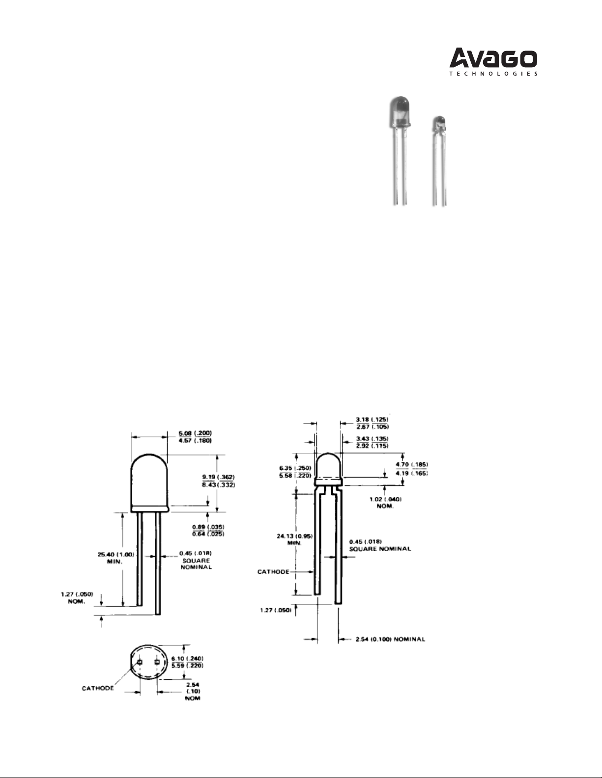
Package Dimensions
Features
• Low power
• High eciency
• CMOS-MOS compatible
• TTL compatible
• Wide viewing angle
• Choice of package styles
• Choice of colors
HLMP-4700, -4719, -4740
A
Notes:
1. All dimensions are in millimetres (inches).
2. An Epoxy Minicus may extend about 1mm (0.040") down the leads
HLMP-1700, -1719, -1790
B
Selection Guide
Device
HLMP-
T-1 3/4 Tinted Diused Red 4700 1.5 2.3 – 50 A
4700-C00xx 1.5 2.3 –
4700-CD0FH 1.5 2.3 4.2
Yellow 4719 0.9 2.1 –
4719-A00xx 0.9 2.1 –
Green 4740 1.0 2.3 –
4740-A00xx 1.0 2.3 –
4740-AB000 1.0 2.3 3.2
T-1 Tinted Diused Red 1700 0.8 2.1 – 50 B
1700-B00xx 0.8 2.1 –
Yellow 1719 0.9 2.1 –
1719-A00xx 0.9 2.1 –
1719-ABB00 0.9 2.1 2.8
Green 1790 1.0 2.3 –
1790-A00xx 1.0 2.3 –
1790-AB0FH 1.0 2.4 3.2
Note:
1. q1/2 is the typical o-axis angle at which the luminous intensity is half the axial luminous intensity.
Luminous Intensity Iv (mcd) at 2 mA
1/2
Package
Outline Package Description Color Min. Typ. Max. 2q
2
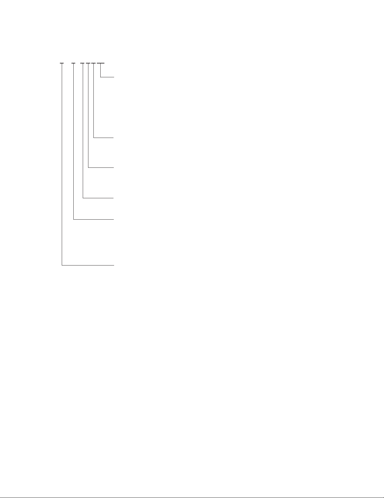
Part Numbering System
HLMP – X 7 XX - X X X XX
Mechanical Option
00: Bulk
01: Tape & Reel, Crimped Leads
02, BH: Tape & Reel, Straight Leads
A1, B1: Right Angle Housing, Uneven Leads
A2, B2: Right Angle Housing, Even Leads
FH: 2 Iv bins select with Inventory Control
Color Bin Options
0: Full color bin distribution
B: Color bins 2 & 3 only
Maximum Iv Bin Options
0: Open (No. max. limit)
Others: Please refer to the Iv bin Table
Minimum Iv Bin Options
Please refer to the Iv Bin Table
Color Options
00: GaP HER
19: GaP Yellow
40: GaP Green
90: GaP Green
Package Options
4: T-1
3
/4 (5 mm)
1: T-1 (3 mm)
3

Electrical/Optical Characteristics at TA = 25°C
Symbol Description T-13/4 T-1 Min. Typ. Max. Units Test Conditions
V
F
VR Reverse Breakdown 4700 1700 5.0 V IR = 50 μA
ld Dominant 4700 1700 626 nm Note 1
Dl
1/2
tS Speed of Response 4700 1700 90 ns
C Capacitance 4700 1700 11 pF VF = 0,
Rq
J-PIN
l
PEAK
hV Luminous Ecacy 4700 1700 145 lumens/watt Note 2
Notes:
1. The dominant wavelength, ld, is derived from the CIE chromaticity diagram and represents the single wavelength which denes the color of the
device.
2. The radiant intensity, Ie, in watts per steradian, may be found from the equation Ie = IV/hV, where IV is the luminous intensity in candelas and hV is
luminous ecacy in lumens/watt.
3. T-13/4.
4. T-1.
Forward Voltage 4700 1700 1.7 2.0 V 2 mA
4719 1719 1.8 2.5
4740 1790 1.9 2.2
Voltage 4719 1719 5.0
4740 1790 5.0
Wavelength 4719 1719 585
4740 1790 569
Spectral Line 4700 1700 40 nm
Halfwidth 4719 1719 36
4740 1790 28
4719 1719 90
4740 1790 500
4719 1719 15 f = 1 MHz
4740 1790 18
Thermal Resistance 4700 1700 260
4719 1719 290
[3]
[4]
°C/W Junction to Cathode
Lead
4740 1790
Peak Wavelength 4700 1700 635 nm Measurement at Peak
4740 1790 565
4719 1719 500
4740 1790 595
4

Absolute Maximum Ratings
DC CURRENT – mA
0
0
VOLTAGE – V
1.5
6
0.5 1.0
2.5
2
4
8
10
2.0
RED
YELLOW
GREEN
RELATIVE LUMINOUS INTENSITY
(NORMALIZED AT 2mA)
0
0
IDC -DC CURRENT PER LED - mA
6
6.0
2 4 10
2.0
4.0
8.0
10.0
8
RED
YELLOW
GREEN
TA - 25°C
YELLOW
WAVELENGTH – nm
RELATIVE INTENSITY
1.0
0.5
0
500 550 600 650 700 750
GREEN
TA = 25° C
RED
Parameter Maximum Rating Units
Power Dissipation
(Derate linearly from 92°C at 1.0 mA/°C)
DC and Peak Forward Current 7 mA
Transient Forward Current (10 μs Pulse)
Reverse Voltage (IR = 50 μA) 5.0 V
Operating Temperature Range Red/Yellow
Storage Temperature Range -40 to +100 °C
Notes:
1. The transient peak current is the maximum non-recurring peak current the devices can withstand without damaging the LED die and wire bonds.
It is not recommended that the device be operated at peak currents beyond the Absolute Maximum Peak Forward Current.
[1]
Red
Yellow
Green
Green
14
17.5
15.4
500 mA
-40 to 100
-20 to 100
mW
°C
°C
Figure 1. Relative intensity vs. wavelength.
Figure 3. Relative luminous intensity vs. forward current.
Figure 2. Forward current vs. forward voltage.
5

Figure 4. Relative luminous intensity vs. angular displacement for T-13/4 lamp.
10° 100°40° 70°20° 60° 80°30° 50° 90°
RELATIVE INTENSITY
1.0
0.8
0.6
0.4
0.2
0.0
0°
10°
40°
70°
20°
60°
80°
30°
50°
90°
10° 100°40° 70°20° 60° 80°30° 50° 90°
RELATIVE INTENSITY
1.0
0.8
0.6
0.4
0.2
0.0
0°
10°
40°
70°
20°
60°
80°
30°
50°
90°
Figure 5. Relative llluminous intensity vs. angular displacement for T-1 lamp.
Intensity Bin Limits
Intensity Range (mcd)
Color Bin Min. Max.
Red B 0.9 1.5
C 1.5 2.4
D 2.4 3.8
E 3.8 6.1
F 6.1 9.7
G 9.7 15.5
H 15.5 24.8
I 24.8 39.6
J 39.6 63.4
K 63.4 101.5
L 101.5 162.4
M 162.4 234.6
N 234.6 340.0
O 340.0 540.0
P 540.0 850.0
Q 850.0 1200.0
R 1200.0 1700.0
S 1700.0 2400.0
T 2400.0 3400.0
U 3400.0 4900.0
V 4900.0 7100.0
W 7100.0 10200.0
X 10200.0 14800.0
Y 14800.0 21400.0
Maximum tolerance for each bin limit is ±18%.
6
Z 21400.0 30900.0
Intensity Bin Limits
Intensity Range (mcd)
Color Bin Min. Max.
Yellow A 1.0 1.6
B 1.6 2.5
C 2.5 4.0
D 4.0 6.5
E 6.5 10.3
F 10.3 16.6
G 16.6 26.5
H 26.5 42.3
I 42.3 67.7
J 67.7 108.2
K 108.2 173.2
L 173.2 250.0
M 250.0 360.0
N 360.0 510.0
O 510.0 800.0
P 800.0 1250.0
Q 1250.0 1800.0
R 1800.0 2900.0
S 2900.0 4700.0
T 4700.0 7200.0
U 7200.0 11700.0
V 11700.0 18000.0
W 18000.0 27000.0
Maximum tolerance for each bin limit is ±18%.

Intensity Bin Limits
Color Categories
Intensity Range (mcd)
Color Bin Min. Max.
Green A 1.1 1.8
B 1.8 2.9
C 2.9 4.7
D 4.7 7.6
E 7.6 12.0
F 12.0 19.1
G 19.1 30.7
H 30.7 49.1
I 49.1 78.5
J 78.5 125.7
K 125.7 201.1
L 201.1 289.0
M 289.0 417.0
N 417.0 680.0
O 680.0 1100.0
P 1100.0 1800.0
Q 1800.0 2700.0
R 2700.0 4300.0
S 4300.0 6800.0
T 6800.0 10800.0
U 10800.0 16000.0
V 16000.0 25000.0
W 25000.0 40000.0
Maximum tolerance for each bin limit is ±18%.
Lambda (nm)
Color Category # Min. Max.
6 561.5 564.5
5 564.5 567.5
Green 4 567.5 570.5
3 570.5 573.5
2 573.5 576.5
1 582.0 584.5
3 584.5 587.0
Yellow 2 587.0 589.5
4 589.5 592.0
5 592.0 593.0
Tolerance for each bin limit is ±0.5 nm.
Mechanical Option Matrix
Mechanical Option Code Denition
00 Bulk Packaging, minimum increment 500 pc/bag
01 Tape & Reel, crimped leads, min. increment 1300 pcs/bag for T-1 3/4, 1800 pcs/bag for T-1
02 Tape & Reel, straight leads, min. increment 1300 pcs/bag for T-1 3/4, 1800 pcs/bag for T-1
A1 T-1, Right Angle Housing, uneven leads, minimum increment 500 pcs/bag
A2 T-1, Right Angle Housing, even leads, minimum increment 500 pcs/bag
B1 T-1 3/4, Right Angle Housing, uneven leads, minimum increment 500 pcs/bag
B2 T-1 3/4, Right Angle Housing, even leads, minimum increment 500 pcs/bag
BH T-1, Tape & Reel, straight leads, minimum increment 2000 pcs/bag
FH Devices that require inventory control and 2 Iv bin select
R1 Tape & Reel, crimped leads, reeled counter clockwise, cathode lead leaving the reel rst
Notes: All categories are established for classication of products. Products may not be available in all categories. Please contact your local Avago
representative for further clarication/information.
7

Precautions:
1.59 mm
Lead Forming:
• The leads of an LED lamp may be preformed or cut to
length prior to insertion and soldering on PC board.
• For better control, it is recommended to use proper
tool to precisely form and cut the leads to applicable
length rather than doing it manually.
• If manual lead cutting is necessary, cut the leads after
the soldering process. The solder connection forms a
mechanical ground which prevents mechanical stress
due to lead cutting from traveling into LED package.
This is highly recommended for hand solder operation,
as the excess lead length also acts as small heat sink.
Soldering and Handling:
• Care must be taken during PCB assembly and soldering
process to prevent damage to the LED component.
• LED component may be eectively hand soldered
to PCB. However, it is only recommended under
unavoidable circumstances such as rework. The closest
manual soldering distance of the soldering heat source
(soldering iron’s tip) to the body is 1.59mm. Soldering
the LED using soldering iron tip closer than 1.59mm
might damage the LED.
• ESD precaution must be properly applied on the
soldering station and personnel to prevent ESD
damage to the LED component that is ESD sensitive.
Do refer to Avago application note AN 1142 for details.
The soldering iron used should have grounded tip to
ensure electrostatic charge is properly grounded.
• Recommended soldering condition:
Wave Manual Solder
Soldering
Pre-heat Temperature 105°C Max. –
Pre-heat Time 60 sec Max. –
Peak Temperature 250°C Max. 260°C Max.
Dwell Time 3 sec Max. 5 sec Max.
Note:
1) Above conditions refers to measurement with thermocouple
mounted at the bottom of PCB.
2) It is recommended to use only bottom preheaters in order to
reduce thermal stress experienced by LED.
[1],[2]
Dipping
• Wave soldering parameters must be set and maintained
according to the recommended temperature and dwell
time. Customer is advised to perform daily check on the
soldering prole to ensure that it is always conforming
to recommended soldering conditions.
Note:
1. PCB with dierent size and design (component density) will have
dierent heat mass (heat capacity). This might cause a change in
temperature experienced by the board if same wave soldering
setting is used. So, it is recommended to re-calibrate the soldering
prole again before loading a new type of PCB.
2. Customer is advised to take extra precaution during wave soldering
to ensure that the maximum wave temperature does not exceed
250°C and the solder contact time does not exceeding 3sec. Overstressing the LED during soldering process might cause premature
failure to the LED due to delamination.
• Any alignment xture that is being applied during
wave soldering should be loosely tted and should
not apply weight or force on LED. Non metal material
is recommended as it will absorb less heat during wave
soldering process.
• At elevated temperature, LED is more susceptible to
mechanical stress. Therefore, PCB must allowed to cool
down to room temperature prior to handling, which
includes removal of alignment xture or pallet.
• If PCB board contains both through hole (TH) LED and
other surface mount components, it is recommended
that surface mount components be soldered on the
top side of the PCB. If surface mount need to be on the
bottom side, these components should be soldered
using reow soldering prior to insertion the TH LED.
• Recommended PC board plated through holes (PTH)
size for LED component leads.
LED Component Plated Through
Lead Size Diagonal Hole Diameter
0.45 x 0.45 mm 0.636 mm 0.98 to 1.08 mm
(0.018 x 0.018 inch) (0.025 inch) (0.039 to 0.043 inch)
0.50 x 0.50 mm 0.707 mm 1.05 to 1.15 mm
(0.020 x 0.020 inch) (0.028 inch) (0.041 to 0.045 inch)
• Over-sizing the PTH can lead to twisted LED after
clinching. On the other hand under sizing the PTH can
cause diculty inserting the TH LED.
Refer to application note AN5334 for more information
about soldering and handling of TH LED lamps.
8

Example of Wave Soldering Temperature Prole for TH LED
0 10 20 30 40 50 60 70 80 90 100
250
200
150
100
50
TIME (MINUTES)
PREHEAT
TURBULENT WAVE
LAMINAR
HOT AIR KNIFE
TEMPERATURE (°C)
Recommended solder:
Sn63 (Leaded solder alloy)
SAC305 (Lead free solder alloy)
Flux: Rosin flux
Solder bath temperature:
245°C± 5°C (maximum peak temperature = 250°C)
Dwell time: 1.5 sec – 3.0 sec (maximum = 3sec)
Note: Allow for board to be sufficiently cooled to
room temperature before exerting mechanical force.
(1P) Item: Part Number
(1T) Lot: Lot Number
LPN:
(9D)MFG Date: Manufacturing Date
(P) Customer Item:
(V) Vendor ID:
DeptID: Made In: Country of Origin
(Q) QTY: Quantity
CAT: Intensity Bin
BIN: Color Bin
(9D) Date Code: Date Code
STANDARD LABEL LS0002
RoHS Compliant
e3 max temp 250C
Packaging Label:
(i) Avago Mother Label: (Available on packaging box of ammo pack and shipping box)
9

(ii) Avago Baby Label (Only available on bulk packaging)
(1P) Item: Part Number
(1T) Lot: Lot Number
LPN:
(9D)MFG Date: Manufacturing Date
(P) Customer Item:
(V) Vendor ID:
DeptID: Made In: Country of Origin
(Q) QTY: Quantity
CAT: Intensity Bin
BIN: Color Bin
(9D) Date Code: Date Code
STANDARD LABEL LS0002
RoHS Compliant
e3 max temp 250C
(1P) PART #: Part Number
(1T) LOT #: Lot Number
(9D)MFG DATE: Manufacturing Date
C/O: Country of Origin
Customer P/N:
Supplier Code:
QUANTITY: Packing Quantity
CAT: Intensity Bin
BIN: Color Bin
DATECODE: Date Code
RoHS Compliant
e3 max tem
p
250C
Lamps Baby Label
For product information and a complete list of distributors, please go to our web site: www.avagotech.com
Avago, Avago Technologies, and the A logo are trademarks of Avago Technologies in the United States and other countries.
Data subject to change. Copyright © 2005-2009 Avago Technologies. All rights reserved. Obsoletes 5989-4256EN
AV02-1557EN - May 5, 2009
 Loading...