


APDS-9300
Miniature Ambient Light Photo Sensor
with Digital (I2C) Output
Data Sheet
Description
The APDS-9300 is a low-voltage Digital Ambient Light
Photo Sensor that converts light intensity to digital signal
output capable of direct I2C interface. Each device consists
of one broadband photodiode (visible plus infrared) and
one infrared photodiode. Two integrating ADCs convert
the photodiode currents to a digital output that represents
the irradiance measured on each channel. This digital output can be input to a microprocessor where illuminance
(ambient light level) in lux is derived using an empirical
formula to approximate the human-eye response.
Application Support Information
The Application Engineering Group is available to assist
you with the application design associated with APDS9300 ambient light photo sensor module. You can contact
them through your local sales representatives for additional details.
Features
• Approximate the human-eye response
• Precise Illuminance measurement under diverse
lighting conditions
• Programmable Interrupt Function with User-Dened
Upper and Lower Threshold Settings
• 16-Bit Digital Output with I2C Fast-Mode at 400 kHz
• Programmable Analog Gain and Integration Time
• Miniature ChipLED Package
Height - 0.55mm
Length - 2.60mm
Width - 2.20mm
• 50/60-Hz Lighting Ripple Rejection
• Low 2.5-V Input Voltage and 1.8-V Digital Output
• Low Active Power (0.6 mW Typical) with Power Down
Mode
• RoHS Compliant
Applications
• Detection of ambient light to control display
backlighting
o Mobile devices – Cell phones, PDAs, PMP
o Computing devices – Notebooks, Tablet PC, Key
board
o Consumer devices – LCD Monitor, Flat-panel TVs,
Video Cameras, Digital Still Camera
• Automatic Residential and Commercial Lighting
Management
• Automotive instrumentation clusters.
• Electronic Signs and Signals
Ordering Information
I2C
Interrupt
ADC Register
Command
Register
Address Select
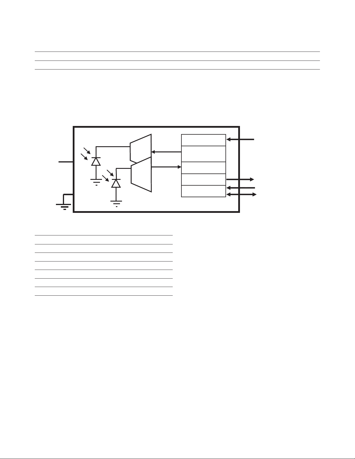
Ch0 (Visible + IR)
Ch1 (IR)
SCL
SDA
ADDR SEL
VDD= 2.4 V
to 3.0 V
INT
ADC
ADC
GND
Part Number Packaging Type Package Quantity
APDS-9300-020 Tape and Reel 6-pins Chipled package 2500
Functional Block Diagram
I/O Pins Conguration Table
Pin Symbol Description
1 V
2 GND Ground
3 ADDR SEL Address Select
4 SCL Serial Clock
5 SDA Serial Data
6 INT Interrupt
DD
2
Voltage Supply

Absolute Maximum Ratings
Parameter Symbol Min Max Unit
Supply voltage V
Digital output voltage range V
Digital output current I
Storage temperature range T
ESD tolerance human body model - 2000 V
DD
O
O
stg
- 3.8 V
-0.5 3.8 V
-1 20 mA
-40 85 ºC
Recommended Operating Conditions
Parameter Symbol Min Typ Max Unit Conditions
Supply Voltage V
Operating Temperature T
SCL, SDA input low voltage V
SCL, SDA input high voltage V
DD
a
IL
IH
2.4 2.5 3.0 V
-30 - 85 ºC
-0.5 - 0.58 V
1.13 - 3.6 V 2.4 ≤ VDD ≤ 2.6
1.25 - 3.6 V 2.4 ≤ VDD ≤ 3.0
Electrical Characteristics
Parameter Symbol Min Typ Max Unit Conditions
Supply current I
INT, SDA output low voltage V
Leakage current I
DD
OL
LEAK
-
-
0
0
0.24
3.2
-
-
0.6
15
0.4
0.6
mA
μA
V
V
-5 - 5 μA
Active
Power down
3 mA sink current
6 mA sink current
3

Operating Characteristics, High Gain (16X), VDD = 2.5 V, Ta = 25 ºC, (unless otherwise noted) (see Notes 2, 3, 4, 5)
Parameter Symbol Channel Min Typ Max Unit Conditions
Oscillator frequency fosc 690 735 780 kHz
Dark ADC count value Ch0 0 4 counts Ee = 0, Tint = 402 ms
Ch1 0 4
Full scale ADC count value
(Note 6)
ADC count value Ch0 750 1000 1250 counts λp = 640 nm, Tint = 101 ms
ADC count value ratio: Ch1/
Ch0
Irradiance responsivity Re Ch0 27.5 counts/
Illuminance responsivity Rv Ch0 36 counts/
ADC count value ratio: Ch1/
Ch0
Illuminance responsivity,
low gain mode (Note 7)
(Sensor Lux) /(actual Lux),
high gain mode (Note 8)
Rv Ch0 2.3 counts/
Ch0 65535 counts Tint > 178 ms
Ch1 65535
Ch0 37177 Tint = 101 ms
Ch1 37177
Ch0 5047 Tint = 13.7 ms
Ch1 5047
Ch1 200 Ee = 36.3 µW/cm2
Ch0 700 1000 1300 λp = 940 nm, Tint = 101 ms
Ch1 820 Ee = 119 µW/cm2
0.15 0.2 0.25 λp = 640 nm, Tint = 101 ms
0.69 0.82 0.95 λp = 940 nm, Tint = 101 ms
λp = 640 nm, Tint = 101 ms
Ch1 5.5
Ch0 8.4 λp = 940 nm, Tint = 101 ms
Ch1 6.9
Ch1 4 Tint = 402 ms
Ch0 144 Incandescent light source:
Ch1 72 Tint = 402 ms
0.11 Fluorescent light source:
0.5 Incandescent light source:
Ch1 0.25 Tint = 402 ms
Ch0 9 Incandescent light source:
Ch1 4.5 Tint = 402 ms
0.65 1 1.35 Fluorescent light source:
0.60 1 1.40 Incandescent light source:
(µW/cm2)
Fluorescent light source:
lux
Tint = 402 ms
Tint = 402 ms
Fluorescent light source:
lux
Tint = 402 ms
Tint = 402 ms
4

Notes:
2. Optical measurements are made using small–angle incident radiation from light–emitting diode optical sources. Visible 640 nm LEDs and infrared
940 nm LEDs are used for nal product testing for compatibility with high–volume production.
3. The 640 nm irradiance Ee is supplied by an AlInGaP light–emitting diode with the following characteristics: peak wavelength lp = 640 nm and
spectral halfwidth Dl½ = 17 nm.
4. The 940 nm irradiance Ee is supplied by a GaAs light–emitting diode with the following characteristics: peak wavelength lp = 940 nm and spectral
halfwidth Dl½ = 40 nm.
5. Integration time Tint, is dependent on internal oscillator frequency (fosc) and on the integration eld value in the timing register as described in
the Register Set section. For nominal fosc = 735 kHz, nominal Tint = (number of clock cycles)/fosc.
Field value 00: Tint = (11 • 918)/fosc = 13.7 ms
Field value 01: Tint = (81 • 918)/fosc = 101 ms
Field value 10: Tint = (322 • 918)/fosc = 402 ms
Scaling between integration times vary proportionally as follows:
11/322 = 0.034 (eld value 00), 81/322 = 0.252 (eld value 01), and 322/322 = 1 (eld value 10).
6. Full scale ADC count value is limited by the fact that there is a maximum of one count per two oscillator frequency periods and also by a 2–count
oset.
Full scale ADC count value = ((number of clock cycles)/2 - 2)
Field value 00: Full scale ADC count value = ((11 • 918)/2 - 2) = 5047
Field value 01: Full scale ADC count value = ((81 • 918)/2 - 2) = 37177
Field value 10: Full scale ADC count value = 65535, which is limited by 16 bit register. This full scale ADC count value is reached for 131074
clock cycles, which occurs for Tint = 178 ms for nominal fosc = 735 kHz.
7. Low gain mode has 16x lower gain than high gain mode: (1/16 = 0.0625).
8. For sensor Lux calculation, please refer to the empirical formula in Application Note. It is based on measured Ch0 and Ch1 ADC count values for the
light source specied. Actual Lux is obtained with a commercial luxmeter. The range of the (sensor Lux) / (actual Lux) ratio is estimated based on
the variation of the 640 nm and 940 nm optical parameters. Devices are not 100% tested with uorescent or incandescent light sources.
CH1/CH0 Sensor Lux Formula
0 ≤ CH1/CH0 ≤ 0.52 Sensor Lux = (0.0315 x CH0) – (0.0593 x CH0 x ((CH1/CH0)
0.52 ≤ CH1/CH0 ≤ 0.65 Sensor Lux = (0.0229 x CH0) – (0.0291 x CH1)
0.65 ≤ CH1/CH0 ≤ 0.80 Sensor Lux = (0.0157 x CH0) – (0.0180 x CH1)
0.80 ≤ CH1/CH0 ≤ 1.30 Sensor Lux = (0.00338 x CH0) – (0.00260 x CH1)
CH1/CH0 ≥ 1.30 Sensor Lux = 0
1.4
))
AC Electrical Characteristics (VDD = 3 V, Ta = 25 ºC)
Parameter † Min. Typ. Max. Unit
t
(CONV)
f
(SCL)
t
(BUF)
t
(HDSTA)
t
(SUSTA)
t
(SUSTO)
t
(HDDAT)
t
(SUDAT)
t
(LOW)
t
(HIGH)
t
F
t
R
C
j
† Specied by design and characterization; not production tested.
Conversion time 12 100 400 ms
Clock frequency - - 400 kHz
Bus free time between start and stop condition 1.3 - - μs
Hold time after (repeated) start condition. After this
0.6 - - μs
period, the rst clock is generated.
Repeated start condition setup time 0.6 - - μs
Stop condition setup time 0.6 - - μs
Data hold time 0 - 0.9 μs
Data setup time 100 - - ns
SCL clock low period 1.3 - - μs
SCL clock high period 0.6 - - μs
Clock/data fall time - - 300 ns
Clock/data rise time - - 300 ns
Input pin capacitance - - 10 pF
5
Parameter Measurement Information
A0A1A2A3A4A5A 6D1D2D3D4D5D6D7D0
R/W
Start by
Master
ACK by
APDS-9300
Stop by
Master
ACK by
APDS-9300
SDA
Frame 1 I2C Slave Address Byte
Frame 2 Command Byte
SCL
1 9 1 9
SDA
SCL
StopStart
SCL
ACK
t
(LOWMEXT)
t
(LOWMEXT)
t
(LOWSEXT)
SCL
ACK
t
(LOWMEXT)
SDA
SCL
Start
Condition
Stop
Condition
P
t
(SUSTO)
t
(SUDAT)
t
(HDDAT)
t
(BUF)
V
IH
V
IL
t
(R)
t
(LOW)
t
(HIGH)
t
(F)
t
(HDSTA)
V
IH
V
IL
P S
S
t
(SUSTA)
A0A1A2A3A4A5A6D1D2D3D4D5D6D7D 0
R/W
Start by
Master
ACK by
APDS-9300
Stop by
Master
NACK by
Master
SDA
Frame 1 I2C Slave Address Byte
Frame 2 Data Byte From APDS-9300
SCL
1 9 1
9
Figure 1. Timing Diagrams
Figure 2. Example Timing Diagram for I2C Send Byte Format
Figure 3. Example Timing Diagram for I2C Receive Byte Format
6
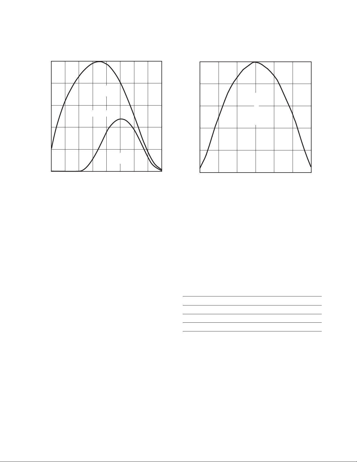
Typical Characteristics
SPECTRAL RESPONSIVITY
0
400
0.2
0.4
0.6
0.8
1
500 600 700 800 900 1000 1100
NORMALIZED RESPONSIVITY
300
CHANNEL 1
PHOTODIODE
CHANNEL 0
PHOTODIODE
- WAVELENGTH - nm
470 pF
ANGULAR DISPLACEMENT - °
NORMALIZED RESPONSIVITY
0
0.2
0.4
0.6
0.8
1.0
-90 -60 -30 0 30 60
90
OPTICAL AXIS
Figure 4. Normalized Responsivity vs. Spectral Responsivity Figure 5. Normalized Responsivity vs. Angular Displacement * CL Package
Principles of Operation
Analog–to–Digital Converter
The APDS-9300 contains two integrating analog–to–digital converters (ADC) that integrate the currents from the
channel 0 and channel 1 photodiodes. Integration of both
channels occurs simultaneously, and upon completion of
the conversion cycle the conversion result is transferred to
the channel 0 and channel 1 data registers, respectively.
The transfers are double buered to ensure that invalid
data is not read during the transfer. After the transfer, the
device automatically begins the next integration cycle.
Digital Interface
Interface and control of the APDS-9300 is accomplished
through a two–wire serial interface to a set of registers
that provide access to device control functions and output data. The serial interface is compatible to I2C bus Fast–
Mode. The APDS-9300 oers three slave addresses that
are selectable via an external pin (ADDR SEL). The slave
address options are shown in Table 1.
Table 1. Slave Address Selection
ADDR SEL Terminal Level Slave Address
GND 0101001
Float 0111001
V
DD
NOTE:
The Slave Addresses are 7 bits and please note the I2C protocols. A read/
write bit should be appended to the slave address by the master device
to properly communicate with the APDS-9300 device.
1001001
7

I2C Protocols
Wr
71 81 1 1 1
Data ByteSlave AddressS A PA
X X
A Acknowledge (this bit position may be 0 for an ACK or 1 for a NACK)
P Stop Condition
Rd Read (bit value of 1)
S Start Condition
Sr Repeated Start Condition
Wr Write (bit value of 0)
X Shown under a field indicates that that field is required to have a value of X
... Continuation of protocol
Master –to–Slave
Slave –to–Master
P
Wr
81 81 1 1 17
Slave AddressS A
A
Command Code Data Byte A
1
P
Wr
1
71 81 1 1 81 17 1 1
Data Byte
Slave AddressS A
A
Command Code Slave Address
A
ASr Rd
P
Wr
1
81 81 1 1 8 17 1
Data Byte High
Slave Address
SAA
Command Code
Data Byte Low
A
A
Wr
71 81 1 1 17 1 1
Slave Address
SAA
Command Code
Slave Address
ASrRd
8 1
Data Byte Low
A
…
P
1
8 1
Data Byte High
A
1
Each Send and Write protocol is, essentially, a series of
bytes. A byte sent to the APDS-9300 with the most signicant bit (MSB) equal to 1 will be interpreted as a COMMAND byte. The lower four bits of the COMMAND byte
form the register select address (see Table 2), which is
used to select the destination for the subsequent byte(s)
received. The APDS-9300 responds to any Receive Byte requests with the contents of the register specied by the
stored register select address.
The APDS-9300 implements the following protocols of
the Philips Semiconductor I2C specication:
• I2C Write Protocol
• I2C Read Protocol
For a complete description of I2C protocols, please review
the I2C Specication athttp://www.semiconductors.philips.com
Figure 6. I2C Packet Protocol Element Key
Figure 7. I2C Write Protocols
Figure 8. I2C Read (Combined Format) Protocols
Figure 9. I2C Write Word Protocols
Figure 10. I2C Read Word Protocols
8

Register Set
The APDS-9300 is controlled and monitored by sixteen registers (three are reserved) and a command register accessed
through the serial interface. These registers provide for a variety of control functions and can be read to determine results of the ADC conversions. The register set is summarized in Table 2.
Table 2. Register Address
Address Register Name Register Function
-- COMMAND Species register address
0h CONTROL Control of basic functions
1h TIMING Integration time/gain control
2h THRESHLOWLOW Low byte of low interrupt threshold
3h THRESHLOWHIGH High byte of low interrupt threshold
4h THRESHHIGHLOW Low byte of high interrupt threshold
5h THRESHHIGHHIGH High byte of high interrupt threshold
6h INTERRUPT Interrupt control
7h -- Reserved
8h CRC Factory test — not a user register
9h -- Reserved
Ah ID Part number/ Rev ID
Bh -- Reserved
Ch DATA0LOW Low byte of ADC channel 0
Dh DATA0HIGH High byte of ADC channel 0
Eh DATA1LOW Low byte of ADC channel 1
Fh DATA1HIGH High byte of ADC channel 1
The mechanics of accessing a specic register depends on the specic I2C protocol used. Refer to the section on I2C
protocols. In general, the COMMAND register is written rst to specify the specic control/status register for following
read/write operations.
9

Command Register
ADDRESSCLEARCMD WORD Resv
67 5 4 23 1 0
00 0 0 00 0 0Reset Value:
COMMAND
POWERResvResv ResvResv Resv Resv
67 5 4 23 1 0
00 0 0 00 0 0Reset Value:
CONTROL
0h
The command register species the address of the target register for subsequent read and write operations. The Send
Byte protocol is used to congure the COMMAND register. The command register contains eight bits as described in
Table 3. The command register defaults to 00h at power on.
Table 3. Command Register
Field BIT Description
CMD 7 Select command register. Must write as 1.
CLEAR 6 Interrupt clear. Clears any pending interrupt.
This bit is a write–one–to–clear bit. It is self clearing.
WORD 5 I2C Write/Read Word Protocol.
1 indicates that this I2C transaction is using either the I2C Write Word or Read Word protocol.
Resv 4 Reserved. Write as 0.
ADDRESS 3:0 Register Address.
This eld selects the specic control or status register for following write and read commands according to Table 2.
Control Register (0h)
The CONTROL register contains two bits and is primarily used to power the APDS-9300 device up and down as shown
in Table 4.
Table 4. Control Register
Field BIT Description
Resv 7:2 Reserved. Write as 0.
POWER 1:0 Power up/power down. By writing a 03h to this register, the device is powered up.
By writing a 00h to this register, the device is powered down.
NOTE: If a value of 03h is written, the value returned during a read cycle will be 03h. This feature can be used to verify that the device is communicating
properly.
10

Timing Register (1h)
INTEGMANUALResvResv GAIN ResvResv
67 5 4 23 1 0
00 0 0 00 1 0Reset Value:
TIMING
1h
The TIMING register controls both the integration time and the gain of the ADC channels. A common set of control bits
is provided that controls both ADC channels. The TIMING register defaults to 02h at power on.
Table 5. Timing Register
Field BIT Description
Resv 7-5 Reserved. Write as 0.
GAIN 4 Switches gain between low gain and high gain modes.
Writing a 0 selects low gain (1x);
Writing a 1 selects high gain (16x).
MANUAL 3 Manual timing control.
Writing a 1 begins an integration cycle.
Writing a 0 stops an integration cycle.
NOTE: This eld only has meaning when INTEG = 11.
It is ignored at all other times.
Resv 2 Reserved. Write as 0.
INTEG 1:0 Integrate time. This eld selects the integration time for each conversion.
Integration time is dependent on the INTEG FIELD VALUE and the internal clock frequency. Nominal integration times
and respective scaling between integration times scale proportionally as shown in Table 6. See Note 5 and Note 6 on
page 4 for detailed information regarding how the scale values were obtained.
Table 6. Integration Time
Integ Field Value Scale Nominal Integration Time
00 0.034 13.7 ms
01 0.252 101 ms
10 1 402 ms
11 -- N/A
The manual timing control feature is used to manually start and stop the integration time period. If a particular integration time period is required that is not listed in Table 6, then this feature can be used. For example, the manual timing
control can be used to synchronize the APDS-9300 device with an external light source (e.g. LED). A start command to
begin integration can be initiated by writing a 1 to this bit eld. Correspondingly, the integration can be stopped by
simply writing a 0 to the same bit eld.
11

Interrupt Threshold Register (2h - 5h)
PERSISTResvResv INTR
67 5 4 23 1 0
00 0 0 00 0 0Reset Value:
INTERRUPT
6h
The interrupt threshold registers store the values to be used as the high and low trigger points for the comparison function for interrupt generation. If the value generated by channel 0 crosses below or is equal to the low threshold specied,
an interrupt is asserted on the interrupt pin. If the value generated by channel 0 crosses above the high threshold specied, an interrupt is asserted on the interrupt pin. Registers THRESHLOWLOW and THRESHLOWHIGH provide the low byte
and high byte, respectively, of the lower interrupt threshold. Registers THRESHHIGHLOW and THRESHHIGHHIGH provide
the low and high bytes, respectively, of the upper interrupt threshold. The high and low bytes from each set of registers
are combined to form a 16–bit threshold value. The interrupt threshold registers default to 00h on power up.
Table 7. Interrupt Threshold Register
Register Address Bits Description
THRESHLOWLOW 2h 7:0 ADC channel 0 lower byte of the low threshold
THRESHLOWHIGH 3h 7:0 ADC channel 0 upper byte of the low threshold
THRESHHIGHLOW 4h 7:0 ADC channel 0 lower byte of the high threshold
THRESHHIGHHIGH 5h 7:0 ADC channel 0 upper byte of the high threshold
NOTE: Since two 8–bit values are combined for a single 16–bit value for each of the high and low interrupt thresholds, the Send Byte protocol
should not be used to write to these registers. Any values transferred by the Send Byte protocol with the MSB set would be interpreted as the
COMMAND eld and stored as an address for subsequent read/write operations and not as the interrupt threshold information as desired. The Write
Word protocol should be used to write byte–paired registers. For example, the THRESHLOWLOW and THRESHLOWHIGH registers (as well as the
THRESHHIGHLOW and THRESHHIGHHIGH registers) can be written together to set the 16–bit ADC value in a single transaction.
Interrupt Control Register (6h)
The INTERRUPT register controls the extensive interrupt capabilities of the APDS-9300. The APDS-9300 permits traditional level–style interrupts. The interrupt persist bit eld (PERSIST) provides control over when interrupts occur. A value
of 0 causes an interrupt to occur after every integration cycle regardless of the threshold settings. A value of 1 results
in an interrupt after one integration time period outside the threshold window. A value of N (where N is 2 through15)
results in an interrupt only if the value remains outside the threshold window for N consecutive integration cycles. For
example, if N is equal to 10 and the integration time is 402 ms, then the total time is approximately 4 seconds.
When a level Interrupt is selected, an interrupt is generated whenever the last conversion results in a value outside of
the programmed threshold window. The interrupt is active–low and remains asserted until cleared by writing the COMMAND register with the CLEAR bit set.
NOTE: Interrupts are based on the value of Channel 0 only.
Table 8. Interrupt Control Register
Field Bits Description
Resv 7:6 Reserved. Write as 0.
INTR 5:4 INTR Control Select. This eld determines mode of interrupt logic according to Table 9,
below.
PERSIST 3:0 Interrupt persistence. Controls rate of interrupts to the host processor as shown in Table 10,
below.
12

Table 9. Interrupt Control Select
REVNOPARTNO
67 5 4 23 1 0
-- - - -- - -Reset Value:
ID
Ah
Intr Field Value Read Value
00 Interrupt output disabled
01 Level Interrupt
Table 10. Interrupt Persistence Select
Persist Field Value Interrupt Persist Function
0000 Every ADC cycle generates interrupt
0001 Any value outside of threshold range
0010 2 integration time periods out of range
0011 3 integration time periods out of range
0100 4 integration time periods out of range
0101 5 integration time periods out of range
0110 6 integration time periods out of range
0111 7 integration time periods out of range
1000 8 integration time periods out of range
1001 9 integration time periods out of range
1010 10 integration time periods out of range
1011 11 integration time periods out of range
1100 12 integration time periods out of range
1101 13 integration time periods out of range
1110 14 integration time periods out of range
1111 15 integration time periods out of range
ID Register (Ah)
The ID register provides the value for both the part number and silicon revision number for that part number. It is a
read–only register, whose value never changes.
Table 11. ID Register
Field Bits Description
PARTNO 7:4 Part Number Identication
REVNO 3:0 Revision number identication
13

ADC Channel Data Registers (Ch - Fh)
The ADC channel data are expressed as 16–bit values spread across two registers. The ADC channel 0 data registers,
DATA0LOW and DATA0HIGH provide the lower and upper bytes, respectively, of the ADC value of channel 0. Registers
DATA1LOW and DATA1HIGH provide the lower and upper bytes, respectively, of the ADC value of channel 1. All channel
data registers are read–only and default to 00h on power up.
Table 12. ADC Channel Data Registers
Register Address Bits Description
DATA0LOW Ch 7:0 ADC channel 0 lower byte
DATA0HIGH Dh 7:0 ADC channel 0 upper byte
DATA1LOW Eh 7:0 ADC channel 1 lower byte
DATA1HIGH Fh 7:0 ADC channel 1 upper byte
The upper byte data registers can only be read following a read to the corresponding lower byte register. When the
lower byte register is read, the upper eight bits are strobed into a shadow register, which is read by a subsequent read
to the upper byte. The upper register will read the correct value even if additional ADC integration cycles end between
the reading of the lower and upper registers.
NOTE: The Read Word protocol can be used to read byte–paired registers. For example, the DATA0LOW and DATA0HIGH registers
(as well as the DATA1LOW and DATA1HIGH registers) may be read together to obtain the 16–bit ADC value in a single transaction
14

APDS-9300 PACKAGE OUTLINE
Pin 1 : V
Pin 2 : GND
Pin 3 : ADDR SEL
Pin 4 : SCL
Pin 5 : SDA
Pin 6 : INT
UNIT: mm
Tolerance: +/- 0.2mm
Notes:
1. All dimensions are in millimeters. Dimension tolerance is ±0.2 mm unless otherwise stated
PCB Pad Layout
The suggested PCB layout is given below:
DD
Notes:
1. All linear dimensions are in millimeters
15

Tape and Reel Dimensions - APDS-9300
16

Moisture Proof Packaging Chart
UNITS IN A SEALED
MOISTURE-PROOF PACKAGE
ENVIRONMENT
LESS THAN 30 °C
AND LESS THAN
60% RH
PACKAGE IS OPENED
(UNSEALED)
PACKAGE IS
OPENED LESS
THAN 168 HOURS
NO BAKING IS
NECESSARY
PERFORM RECOMMENDED
BAKING CONDITIONS
YES
YES
NO
NO
All APDS-9300 options are shipped in moisture proof package. Once opened, moisture absorption begins.
This part is compliant to JEDEC Level 3.
BAKING CONDITIONS CHART
Recommended Storage Conditions
Storage Temperature 10°C to 30°C
Relative Humidity Below 60% RH
Time from Unsealing to Soldering
After removal from the bag, the parts should be soldered
within seven days if stored at the recommended storage
conditions. When MBB (Moisture Barrier Bag) is opened
and the parts are exposed to the recommended storage
conditions more than seven days the parts must be baked
before reow to prevent damage to the parts.
Baking conditions
If the parts are not stored per the recommended storage
conditions they must be baked before reow to prevent
damage to the parts.
Package Temp. Time
In Reels 60°C 48 hours
In Bulk 100°C 4 hours
Note: Baking should only be done once.
17

Recommended Reow Prole
50
100 150 200 250 300
t-TIME
(SECONDS)
25
80
120
150
180
200
230
255
0
T - TEMPERATURE (°C)
R1
R2
R3
R4
R5
217
MAX 260°C
60 sec to 90 sec
Above 217°C
P1
HEAT
UP
P2
SOLDER PASTE DRY
P3
SOLDER
REFLOW
P4
COOL DOWN
Process Zone Symbol DT
Heat Up P1, R1 25°C to 150°C 3°C/s
Solder Paste Dry P2, R2 150°C to 200°C 100s to 180s
Solder Reow P3, R3 200°C to 260°C 3°C/s
Cool Down P4, R5 200°C to 25°C -6°C/s
Time maintained above liquidus point , 217°C > 217°C 60s to 90s
Peak Temperature 260°C -
Time within 5°C of actual Peak Temperature - 20s to 40s
Time 25°C to Peak Temperature 25°C to 260°C 8mins
Maximum DT/Dtime
or Duration
P3, R4 260°C to 200°C -6°C/s
The reow prole is a straight-line representation of a
nominal temperature prole for a convective reow solder process. The temperature prole is divided into four
process zones, each with dierent DT/Dtime temperature
change rates or duration. The DT/Dtime rates or duration
are detailed in the above table. The temperatures are
measured at the component to printed circuit board connections.
In process zone P1, the PC board and component pins are
heated to a temperature of 150°C to activate the ux in
the solder paste. The temperature ramp up rate, R1, is limited to 3°C per second to allow for even heating of both
the PC board and component pins.
Process zone P2 should be of sucient time duration (100
to 180 seconds) to dry the solder paste. The temperature
is raised to a level just below the liquidus point of the solder.
18
Process zone P3 is the solder reow zone. In zone P3, the
temperature is quickly raised above the liquidus point of
solder to 260°C (500°F) for optimum results. The dwell time
above the liquidus point of solder should be between 60
and 90 seconds. This is to assure proper coalescing of the
solder paste into liquid solder and the formation of good
solder connections. Beyond the recommended dwell time
the intermetallic growth within the solder connections
becomes excessive, resulting in the formation of weak
and unreliable connections. The temperature is then rapidly reduced to a point below the solidus temperature of
the solder to allow the solder within the connections to
freeze solid.
Process zone P4 is the cool down after solder freeze. The
cool down rate, R5, from the liquidus point of the solder to
25°C (77°F) should not exceed 6°C per second maximum.
This limitation is necessary to allow the PC board and
component pins to change dimensions evenly, putting
minimal stresses on the component.
It is recommended to perform reow soldering no more
than twice.

Appendix A: Window Design Guide
Z
L
T
D1
Top View
APDS-9300
Photo Light Sensor
WD
D2 D1
D2
A1: Optical Window Dimensions
To ensure that the performance of the APDS-9300 will not
be aected by improper window design, there are some
criteria requested on the dimensions and design of the
window. There is a constraint on the minimum size of the
window, which is placed in front of the photo light sensor,
so that it will not aect the angular response of the APDS-
9300. This minimum dimension that is recommended will
ensure at least a ±35° light reception cone.
If a smaller window is required, a light pipe or light guide
can be used. A light pipe or light guide is a cylindrical
piece of transparent plastic, which makes use of total internal reection to focus the light.
The thickness of the window should be kept as minimum
as possible because there is a loss of power in every optical
window of about 8% due to reection (4% on each side)
and an additional loss of energy in the plastic material.
Figure A1 illustrates the two types of window that we
have recommended which could either be a at window
or a at window with light pipe.
Table A1 and Figure A2 show the recommended dimensions of the window. These dimension values are based
on a window thickness of 1.0mm with a refractive index
1.585.
The window should be placed directly on top of the light
sensitive area of APDS-9300 (see Figure A3) to achieve
better performance. If a at window with a light pipe is
used, dimension D2 should be 1.55mm to optimize the
performance of APDS-9300.
Figure A1. Recommended Window Design
WD: Working Distance between window front panel & APDS-9300
D1: Window Diameter
T: Thickness
L: Length of Light Pipe
D2: Light Pipe Diameter
Z: Distance between window rear panel and APDS-9300
All dimensions are in mm
Figure A2. Recommended Window Dimensions
19

Table A1. Recommended dimension for optical window
WD
(T+L+Z)
Flat Window
(L=0.0 mm, T=1.0 mm)
Z D1 D1 L
Flat window with Light Pipe
(D2=1.55mm, Z =0.5mm, T=1.0mm)
1.5 0.5 2.25 - -
2.0 1.0 3.25 - -
2.5 1.5 4.25 - -
3.0 2.0 5.00 2.5 1.5
6.0 5.0 8.50 2.5 4.5
Figure A3. APDS-9300 Light Sensitive Area
Notes:
1. All dimensions are in millimeters
2. All package dimension tolerance in ± 0.2mm unless otherwise specied
A2: Optical Window Material
The material of the window is recommended to be polycarbonate. The surface nish of the plastic should be
smooth, without any texture.
The recommended plastic material for use as a window is
available from Bayer AG and Bayer Antwerp N. V. (Europe),
Bayer Corp.(USA) and Bayer Polymers Co., Ltd. (Thailand),
as shown in Table A2.
20
Table A2. Recommended Plastic Materials
Visible light
Material number
Makrolon LQ2647 87% 1.587
Makrolon LQ3147 87% 1.587
Makrolon LQ3187 85% 1.587
transmission Refractive index

Appendix B: Application circuit
APDS-9300
Pin 1: V
DD
Pin 5
Pin 4
V
IO
Pin 6
Pin 2: GND
0.1uF
Pin 3
** ADDR_SEL
INT
SDA
SCL
Pin 1
Pin 2
MCU
** Note:
ADDR_SEL Float : Slave address is 0111001
R1
R2
R3
Figure B1. Application circuit for APDS-9300
The power supply lines must be decoupled with a 0.1 uF
capacitor placed as close to the device package as possible, as shown in Figure B1. The bypass capacitor should
have low eective series resistance (ESR) and low eective series inductance (ESI), such as the common ceramic
types, which provide a low impedance path to ground at
high frequencies to handle transient currents caused by
internal logic switching.
Pull-up resistors, R1 and R2, maintain the SDA and SCL
lines at a high level when the bus is free and ensure the
signals are pulled up from a low to a high level within the
required rise time. For a complete description of I2C maximum and minimum R1 and R2 values, please review the
I2C Specication at http://www.semiconductors.philips.
com.
A pull-up resistor, R3, is also required for the interrupt
(INT), which functions as a wired-AND signal in a similar
fashion to the SCL and SDA lines. A typical impedance
value between 10 kΩ and 100 kΩ can be used.
For product information and a complete list of distributors, please go to our web site: www.avagotech.com
Avago, Avago Technologies, and the A logo are trademarks of Avago Technologies Limited in the United States and other countries.
Data subject to change. Copyright © 2008 Avago Technologies Limited. All rights reserved.
AV02-1077EN - March 11, 2008
 Loading...