

Page 1
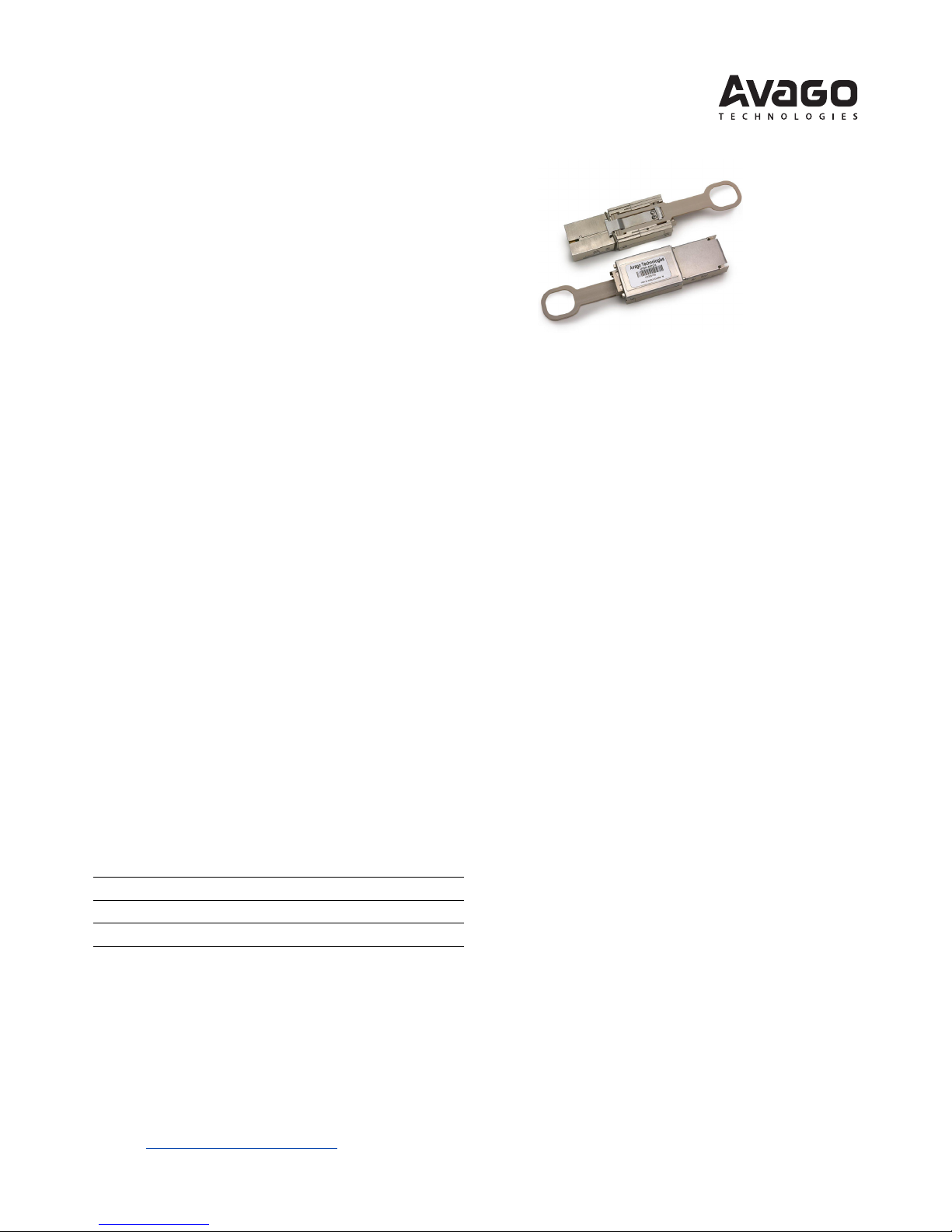
AFBR-83CDZ
12 Channel × 12.5 Gbps Transceiver
CXP Pluggable, Parallel Fiber-Optics Module
Data Sheet
Description
The Avago Technologies AFBR-83CDZ is a Twelve-Channel, Pluggable, Parallel, Fiber-Optic CXP Transceiver for
12 × 12.5G proprietary application. This transceiver is a
high performance module for short-range multi-lane
data communication and interconnect applications. It
integrates twelve data lanes in each direction with 150
Gbps aggregate bandwidth. Each lane can operate at
12.5 Gbps up to 50 m using OM3 ber and 65 m using
OM4 ber. These modules are designed to operate over
multimode ber systems using a nominal wavelength of
850 nm. The electrical interface uses an 84-contact edge
type connector. The optical interface uses a 24-ber MTP
(MPO) connector. This module incorporates Avago Technologies proven integrated circuit and VCSEL technology
to provide reliable long life, high performance, and consistent service.
Applications
• 12 × 12.5G proprietary interconnects
• Data Aggregation, Backplane and Proprietary Protocol
and Density Applications
• Datacom/Telecom switch & router connections
Part Number Ordering Options
AFBR-83CDZ 12x 12.5 Gbps with Full Diagnostic Monitoring
AFBR-83EVB CXP Evaluation Board
AFBR-83EVK* CXP Evaluation Kit
* Includes GUI, User Guide, i-Port and Power Supply
Features
• Compliant to SFF-8642: Mini Multilane Series: Shielded
Integrated Connector, and InniBand Architecture
Specication V2 R1.3 for CXP Interface
• Multi-rate capable from 11 Gbps to 12.5 Gbps
• High Channel Capacity: 150 Gbps per module, bi-
directional, with twelve independent Transmitters and
Receivers each
• Operates at 12.5 Gbps per channel with 64b/66b
encoded data for proprietary application
• Hot Pluggable
• Links up to 50 m using OM3 ber and 65 m using OM4
ber
• 0 to 70 °C case temperature operating range
• 3.3 V power supply only
• Low power dissipation of < 3.5 W
• Proven High Reliability 850 nm technology: Avago
VCSEL array transmitter and Avago PIN array receiver
• Two Wire Serial (TWS) inter face with maskable interrupt
for expanded functionality including:
– Individual channel functions: channel/output dis-
able, squelch disable, and lane polarity inversion
– Diagnostic Monitoring functions: module tempera-
ture and supply voltages, per channel laser current
and laser power, and input receiver power
– Status per channel: Tx fault, electrical (transmitter)
and optical (receiver) LOS, and alarm ags
• Utilizes a standard 24 lane optical ber with MTP
(MPO) optical connector for high density and thin,
light-weight cable management
Patent - www.avagotech.com/patents
Avago Technologies Condential
Page 2

WARNING
CAUTION! Viewing the laser output with certain optical instruments (for
INVISIBLE LASER RADIATION
DO NOT VIEW DIRECTLY
WITH OPTICAL INSTRUMENTS
CLASS 1M LASER PRODUCT
example, eye loupes, magniers and microscopes) within a distance of
100 mm may pose an eye hazard.
CAUTION! Use of controls or adjustments or performance of procedures
other than those specied herein may result in hazardous radiation
exposure.
Note: Standard used for classication: EN 60825-1:2007
CLASS 1M LASER PRODUCT: INVISIBLE LASER RADIATION, DO NOT VIEW DIRECTLY WITH OPTICAL INSTRUMENTS
Transmitter
The optical transmitter incorporates a 12-channel VCSEL
(Vertical Cavity Surface Emitting Laser) array, a 12-channel
input buer and laser driver, diagnostic monitors, and
control and bias blocks. The transmitter is designed for
EN 60825 and CDRH eye safety compliance. The Tx Input
Buer provides dierential inputs presenting a nominal
dierential input impedance of 100 Ohms. AC coupling
capacitors are located inside the CXP module and are not
required on the host board. For module control and interrogation, the control interface incorporates a Two Wire
Serial (TWS) interface of clock and data signals.
Modules have monitors for VCSEL bias, light output power
(LOP), temperature, and power supply voltage implemented; real-time results are available through the TWS interface.
Alarm thresholds are established for the monitored
attributes. Flags are set and interrupts generated when the
attributes are outside the thresholds.
Over the TWS interface, the user can, for individual
channels, control (ip) polarity of the dierential inputs,
de-activate channels, disable the squelch function and
program input equalization levels to reduce the eect of
long PCB traces.
Flags are also set and interrupts generated for loss of input
signal (LOS) and transmitter fault conditions. All ags are
latched and will remain set even if the condition initiating
the latch clears and operation resumes. All interrupts can
be masked and ags are reset by reading the appropriate
ag register.
The optical output will AC squelch for loss of input signal
unless squelch is disabled. The input thresholds for the Tx
squelch are tied to Tx LOS thresholds which are informative only. See Tx LOS thresholds specication on page 6.
Fault detection or channel deactivation through the TWS
interface will disable the channel. Status, alarm and fault
information are available via the TWS interface. To reduce
the need for polling, the hardware interrupt signal is
provided to inform hosts of an assertion of an alarm, LOS
and/or Tx fault.
Receiver
The optical receiver incorporates a 12-channel PIN photodiode array, a 12-channel pre-amplier and output buer,
diagnostic monitors, and control and bias blocks. The Rx
Output Buer provides dierential outputs for the high
speed electrical interface presenting nominal single-ended output impedances of 50 W to AC ground and 100 W
dierentially that should be dierentially terminated with
100 W. AC coupling capacitors are located inside the CXP
module and are not required on the host board.
Modules have a monitor for optical input power; results
are available through the TWS interface. Alarm thresholds
are established for the monitored attributes. Flags are set
and interrupts generated when the attributes are outside
the thresholds.
Over the TWS interface, the user can, for individual
channels, control (ip) polarity of the dierential outputs,
de-activate channels, disable the squelch function,
program output signal amplitude and deemphasis.
Flags are also set and interrupts generated for loss of
optical input signal (LOS). All ags are latched and will
remain set even if the condition initiating the latch clears
and operation resumes. All interrupts can be masked and
ags are reset upon reading the appropriate ag register.
The electrical output will squelch for loss of input signal
(unless squelch is disabled) and channel de-activation
through TWS interface. Status and alarm information are
available via the TWS interface. To reduce the need for
polling, the hardware interrupt signal is provided to inform
hosts of an assertion of an alarm and/or LOS.
2
Avago Technologies Condential
Page 3

High Speed Electrical Signal Interface
Regulatory & Compliance
TX
TX[0-11]p/n are the CXP module transmitter electrical
data inputs and are internally AC coupled (0.1 mF) differential lines with 100 W dierential terminations. AC
coupling capacitors exist inside the CXP module and are
not required on the host board. All transmitter electrical
input channels are compliant to module CPPI specications per IEEE 802.3ba other than jitter tolerance performance as per specied in the Transmitter Electrical Characteristics section of this data sheet.
RX
Rx[0-11]p/n are the CXP module receiver electrical data
outputs and are internally AC coupled (0.1 mF) dierential lines that should be terminated with 100 W dierential at the host side. AC coupling capacitors exist inside
the CXP module and are not required on the host board.
All receiver electrical output channels are compliant to
module CPPI specications per IEEE 802.3ba other than
jitter output performance and output dierential voltage
swing as per specied in the Receiver Electrical Characteristics section of this data sheet.
Tx Equalization Control
Tx Input Equalization Control: Four bit code blocks (bits
7-4 or 3-0) are assigned to each channel.
• Codes 1xxxb are reserved.
• Writing 0111b calls for full-scale equalization.
• Writing 0000b calls for no equalization.
Intermediate code values call for intermediate levels of
equalization.
Various standard and regulations apply to the modules.
These include eye-safety, EMC, ESD and RoHS. See the
Regulatory Section for details regarding these and
component recognition.
Handling and Cleaning
The transceiver module can be damaged by exposure to
current surges and over voltage events. Care should be
taken to restrict exposure to the conditions dened in
the Absolute Maximum Ratings. Wave soldering, reow
soldering and/or aqueous wash process with the modules
on board are not recommended. Normal handling precautions for electrostatic discharge sensitive devices should
be observed.
Each module is supplied with an inserted port plug for
protection of the optical ports. This plug should always be
in place whenever a ber cable is not inserted.
The optical connector includes recessed elements that
are exposed whenever a cable or port plug is not inserted.
Prior to insertion of a ber optic cable, it is recommended
that the cable end be cleaned to avoid contamination from
the cable plug. The port plug ensures the optics remains
clean and no additional cleaning should be needed. In the
event of contamination, dry nitrogen or clean dry air at
less than 20 psi can be used to dislodge the contamination. The optical port features (e.g. guide pins) preclude
use of a solid instrument. Liquids are also not advised.
Rx De-emphasis Control
Rx Output de-Emphasis Control: Four bit code blocks (bits
7-4 or 3-0) are assigned to each channel.
• Codes 1xxxb are reserved.
• Writing 0111b calls for full-scale de-emphasis.
• Writing 0000b calls for minimum de-emphasis.
Writing intermediate code values calls for intermediate
levels of de-emphasis.
3
Avago Technologies Condential
Page 4
Link Model and Reference Channel
Optical Patch Cord
Electrical Connector
TP1
TP0
TP1a
TP4a
TP4
TP5
TP2
TP3
Electrical Connector
ASIC
ASIC
CXP TX
CXP RX
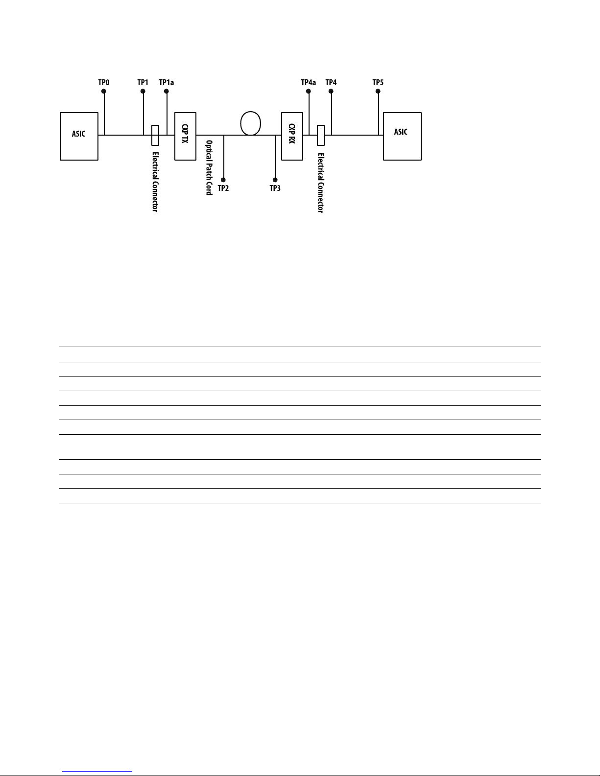
Figure 1. Link Model test point denitions
Absolute Maximum Ratings
Stress in excess of any of the individual Absolute Maximum Ratings can cause immediate catastrophic damage to the
module even if all other parameters are within Recommended Operation Conditions. It should not be assumed that
limiting values of more than one parameter can be applied to the module concurrently. Exposure to any of the Absolute
Maximum Ratings for extended periods can adversely aect reliability.
Parameter Symbol Min Max Units Notes
Storage Temperature Ts -40 85 °C
Absolute Maximum Operating Temperature 85 °C Note 1
3.3 V Power Supply Voltage Vcc33 -0.5 4.0 V
Data Input Voltage – Single Ended -0.5 Vcc33+0.5, 4.0 V
Data Input Voltage – Dierential |V
Control Input Voltage Vi -0.5 Vcc33+0.5
Control Output Current Io -20 20 mA
Relative Humidity RH 5 85 %
Receiver Damage Threshold 4 dBm
Notes:
1. Electro-optical specications are not guaranteed outside the recommended operating temperature range. Operation at or above the maximum
Absolute Maximum Case Temperature for extended periods may adversely aect reliability.
2. This is the maximum voltage that can be applied across the dierential inputs without damaging the input circuitry.
3. The maximum limit is the lesser of Vcc33 + 0.5 V or 4.0 V
dip
- V
| 1.6 V Note 2
din
V Note 3
4.0
4
Avago Technologies Condential
Page 5

Recommended Operating Conditions
Recommended Operating Conditions specify parameters for which the electrical characteristics hold unless otherwise
noted. Electrical characteristics are not dened for operation outside the Recommended Operating Conditions, reliability is not implied and damage to the module may occur for such operation over an extended period of time.
Parameter Symbol Min Typ Max Units Notes
Case Temperature Tc 0 70 °C
3.3 V Power Supply Voltage Vcc33 3.135 3.3 3.465 V
Signal Rate per Channel 12.5 GBd Note 1
Control Input Voltage High Vih 2.3 3.6 V
Control Input Voltage Low Vil -0.3 0.4 V
Host Electrical Compliance
TJ Jitter output (TP1a)
DJ Jitter output (TP1a)
RJ Jitter output (TP1a)
TJ Jitter tolerance (TP4)
DJ Jitter tolerance (TP4)
RJ Jitter tolerance (TP4)
Fiber Length: 4700 MHz•km 50 mm MMF (OM4)
Fiber Length: 2000 MHz•km 50 mm MMF (OM3)
Receiver Dierential Data Output Load
Note:
1. For applications other than 12.5 Gbps per channel, please contact Avago Sales.
2. Per IEEE 802.3ba-2010 TP1a and TP4 CPPI specications for host except for jitter.
3. 1.5dB allocated for connection and splice loss.
0.75
0.45
0.30
100
0.25
0.15
0.10
65
50
UI
UI
UI
UI
UI
UI
m
m
W
Note 2
Note 3
Transceiver Electrical Characteristics
The following characteristics are dened over the Recommended Operating Conditions unless otherwise noted. Typical
values are for Tc = 40°C, Vcc33 = 3.3 V
Parameter Symbol Min Typ Max Units Notes
Transceiver Power Consumption 3.5 W With module
default settings
Transceiver Power Supply Current – Vcc33 1.1 A With module
default settings
Maximum inrush current 1.25 A On any contact
Maximum current ramp rate 100
Power Supply Noise including ripple 50 mVpp Note 1
Power On Initialization Time t
Two Wire Serial Interface Clock Rate 400 kHz
TWS Write Cycle Time (4 byte write) 40 ms
Note:
1. 1 kHz to frequency of operation at the host supply side of the recommended power supply lter with the module and recommended lter in place.
See Figure 9 for recommended power supply lter.
pwr init
2000 ms
mA/ms
5
Avago Technologies Condential
Page 6
Transmitter Electrical Characteristics
The following characteristics are dened over the Recommended Operating Conditions unless otherwise noted. Typical
values are for Tc = 40°C, Vcc33 = 3.3 V
Parameter Symbol Min Typ Max Units Notes
Dierential Input Impedance 80 100 120
LOS Assert Threshold: Tx Data Input
ΔVdi pp losA
110 mVpp Note 1
Dierential Peak-to-Peak Voltage Swing
LOS De-Assert Threshold: Tx Data Input
ΔVdi pp losD
130 210 mVpp Note 1
Dierential Peak-to-Peak Voltage Swing
LOS Hysteresis 0.5 4 dB
Parameter Test Point Min Typ Max Units Notes/Conditions
Single ended input voltage tolerance TP1a -0.3 4.0 V Note 2
AC common mode input voltage tolerance TP1a 15 mV RMS
Dierential input return loss TP1 footnote dB 10 MHz to 11.1 GHz
Dierential to common-mode
input return loss
TJ Jitter tolerance TP1a 0.25 UI
DJ Jitter tolerance TP1a 0.15 UI
RJ Jitter tolerance TP1a 0.10 UI
Data Dependent Pulse Width Shrinkage
(DDPWS) tolerance
Eye Mask Coordinates:
X1, X2, Y1, Y2
Notes:
1. At default Tx EQ setting only. Informative only. Tx LOS thresholds also represent the Tx channel squelch thresholds when enabled. Behavior per
IBTA Annex A6 CXP Interface Specication (Tx squelch disabled).
2. Referred to TP1 signal common; The single-ended input voltage tolerance is the allowable range of the instantaneous input signals
3. From 10 MHz to 11.1 GHz, the magnitude in decibels of the module dierential input return loss at TP1 and the host dierential output return loss
at TP1a shall not exceed the limit given in Equation
Return_loss (ƒ) ≥ 12 – 2√ ƒ 0.01 ≤ ƒ< 4.1 GHz
ƒ
≥ 6.3 – 13log10 4.11 ≤ ƒ< 11.1 GHz
Return_loss(ƒ) is the return loss at frequency ƒ
ƒ is the frequency in GHz.
5.5
TP1 10 dB 10 MHz to 11.1 GHz
TP1a 0.07 UI
TP1a SPECIFICATION VALUES
0.11, 0.31
95, 350
W
UI
mV
Informative
Informative
Note 3
Hit Ratio = 5x10
-5
Y2
Y1
0
-Y1
Differential amplitude (mV)
-Y2
X1
0
X2 1-X2
Time (UI)
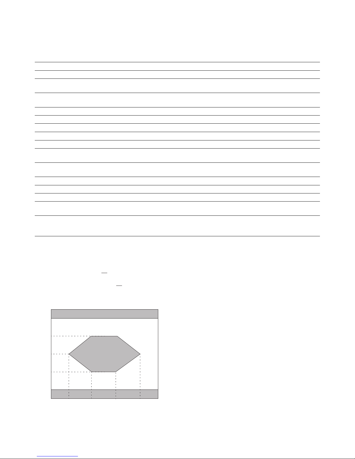
Figure 2. Tx Electrical Eye Mask Coordinates (TP1a) at Hit ratio 5 x 10⁻⁵ hits per sample
6
1-X1
1
Avago Technologies Condential
Page 7
Receiver Electrical Characteristics
The following characteristics are dened over the Recommended Operating Conditions, with module default settings,
unless otherwise noted. Typical values are for Tc = 40°C, Vcc33 = 3.3 V
Parameter Test Point Min Typ Max Units Notes/Conditions
Data Output Dierential Peak-to-Peak
Voltage Swing
AC common mode voltage (RMS) TP4 7.5 mV RMS
Termination mismatch at 1MHz TP4 5 %
Dierential output return loss TP4 footnote 10 MHz to 11.1 GHz
Common-mode output return loss TP4 footnote 10 MHz to 11.1 GHz
Output transition time 20% to 80% TP4 28 ps
TJ Jitter output TP4 0.75 UI
DJ Jitter output TP4 0.45 UI
RJ Jitter output TP4 0.30 UI
Data Dependent Pulse Width Shrinkage
(DDPWS)
Eye Mask coordinates:
X1, X2, Y1, Y2
Notes:
1. From 10 MHz to 11.1 GHz, the magnitude in decibels of the module dierential output return loss at TP4 and the host dierential input return loss
at TP4a shall not exceed the limit given in Equation
Return_loss (ƒ) ≥ 12 – 2√ ƒ 0.01 ≤ ƒ< 4.1 GHz
≥ 6.3 – 13log10 4.11 ≤ ƒ< 11.1 GHz
2. From 10 MHz to 11.1 GHz, the magnitude in decibels of the module common-mode output return loss at TP4 shall not exceed the limit given in
Equation
Return_loss (ƒ) ≥ 7 – 1.6ƒ 0.01 ≤ ƒ< 2.5 GHz
≥ 3 2.5 ≤ ƒ< 11.1 GHz
ƒ
5.5
TP4 220 850 mV
TP4 0.34 UI
TP4 SPECIFICATION VALUES
0.29, 0.5
110, 425
UI
mV
Note 1
Note 2
Hit Ratio = 5x10
-5
Y2
Y1
0
-Y1
Differential Amplitude [mV]
-Y2
0 X1 X2 1-X1 1.0
Normalized Time [UI]
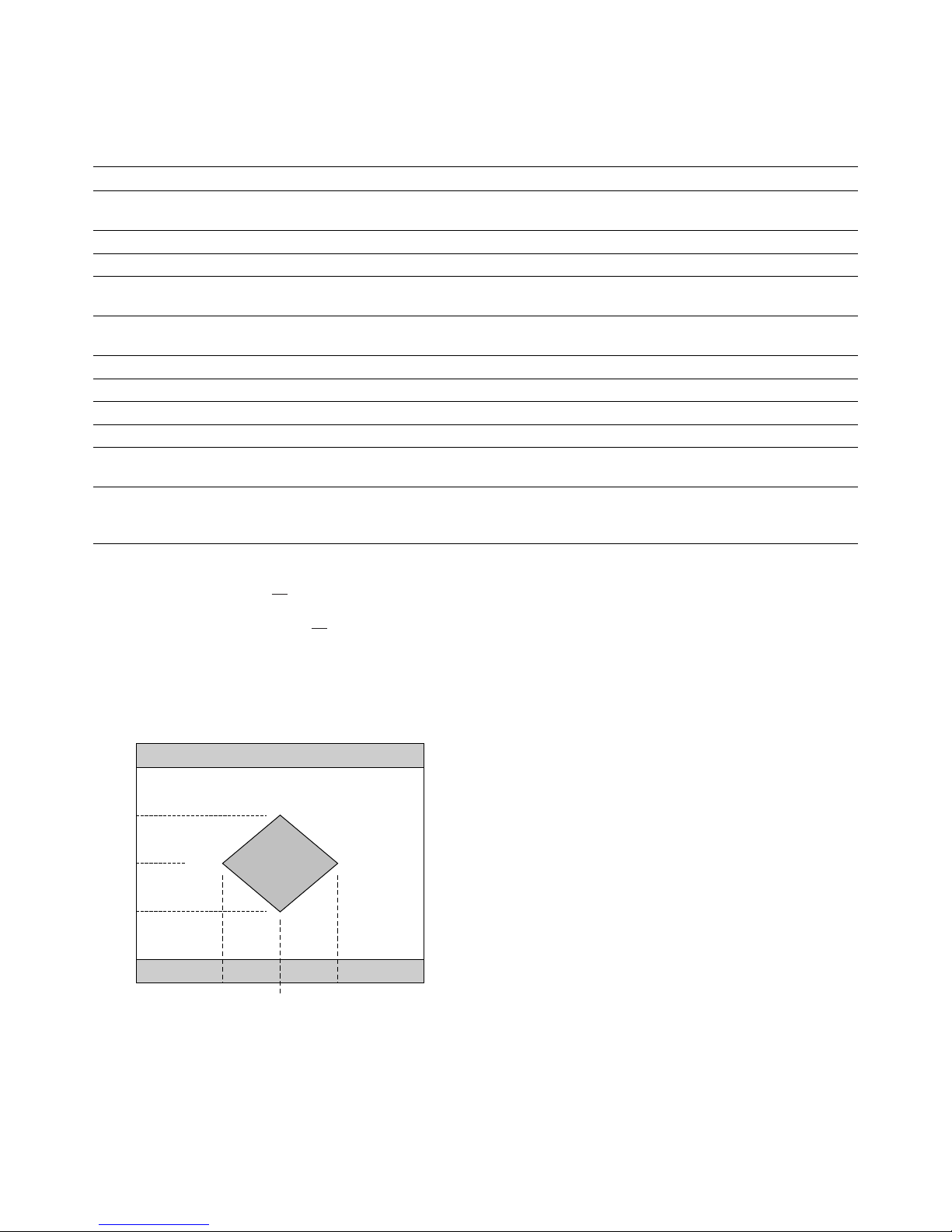
Figure 3. Rx Electrical Eye Mask Coordinates (TP4) at Hit ratio 5 x 10⁻⁵ hits per sample
7
Avago Technologies Condential
Page 8
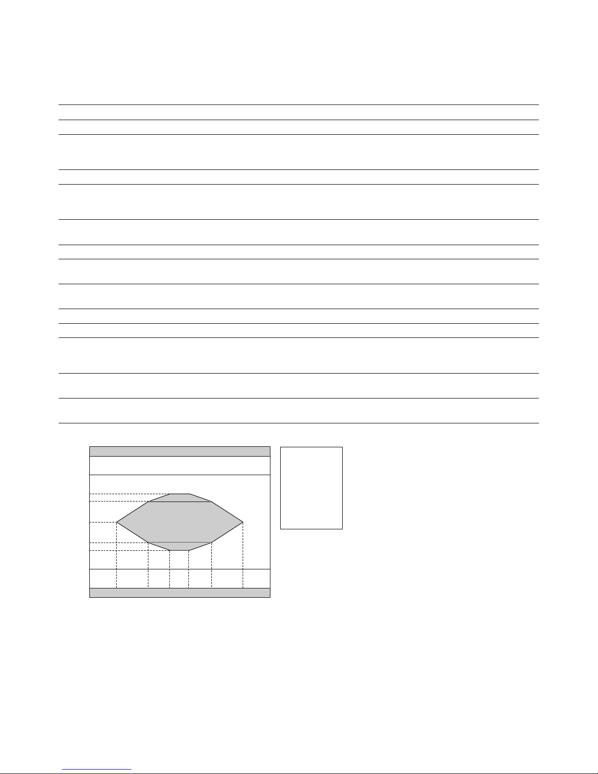
Transmitter Optical Characteristics
The following characteristics are dened over the Recommended Operating Conditions unless otherwise noted. Typical
values are for Tc = 40°C, Vcc33 = 3.3 V
Parameter Test Point Min Typ Max Units Notes/Conditions
Center wavelength TP2 840 850 860 nm
RMS spectral width TP2 0.65 nm RMS Spectral Width is the
standard deviation of the
spectrum
Average launch power, each lane TP2 -7.6 2.4 dBm
Optical Modulation Amplitude (OMA)
each lane
Dierence in launch power between
any two lanes (OMA)
Peak power, each lane TP2 4 dBm
Launch power in OMA minus TDP,
each lane
Transmitter and dispersion penalty (TDP),
each lane
Extinction ratio TP2 3 dB
Optical return loss tolerance TP2 12 dB
Encircled ux TP2
Eye Mask coordinates:
X1, X2, X3, Y1, Y2, Y3
Average launch power of OFF transmitter,
each lane
TP2 -5.6 3 dBm Even if the TDP<0.9 dB,
the OMA minimum must
exceed this minimum value
TP2 4 dB
TP2 -6.5 dBm
TP2 3.5 dB
≥ 86% at 19 mm,
≤ 30% at 4.5 mm
TP2 SPECIFICATION VALUES
0.23, 0.34, 0.43, 0.27, 0.35, 0.4
TP2 -30 dBm
UI Hit Ratio = 5x10
If measured into type A1a.2
50 mm ber in accordance
with EN 61280-1-4
-5
1+Y3
1
1-Y1
1-Y2
0.5
Y2
Y1
Normalizd Amplitude
0
-Y3
0 X1 X2 1-X2 1-X1 1.0X3 1-X3
Normalized Time (Unit Interval
Figure 4. Transmitter eye mask denitions (TP2) at Hit ratio 5 x 10⁻⁵ hits per sample
8
Avago Technologies Condential
Mask Coordinates
X1 = 0.23
X2 = 0.34
X3 = 0.43
Y1 = 0.27
Y2 = 0.35
Y3 = 0.40
Page 9
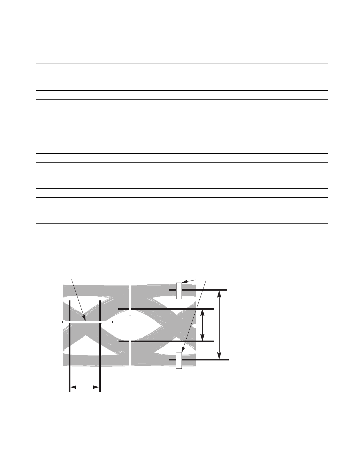
Receiver Optical Characteristics
The following characteristics are dened over the Recommended Operating Conditions unless otherwise noted. Typical
values are for Tc = 40°C, Vcc33 = 3.3 V
Parameter Test Point Min Typ Max Units Notes/Conditions
Center wavelength, each lane TP3 840 850 860 nm
Damage Threshold TP3 3.4 dBm Note 1
Average power at receiver input, each lane TP3 -9.5 2.4 dBm
Receiver Reectance TP3 -12 dB
Optical Modulation Amplitude (OMA),
each lane
Stressed receiver sensitivity in OMA,
each lane
Peak power, each lane TP3 4 dBm
Conditions of stressed receiver sensitivity: TP3 Note 2
Vertical Eye Closure Penalty, each lane TP3 3.5 dB
Stressed eye J2, Jitter, each lane TP3 0.30 UI
Stressed eye J9, Jitter, each lane TP3 0.47 UI
OMA of each aggressor lane TP3 -0.4 dBm
Rx LOS Assert Threshold TP3 -30 dBm OMA
Rx LOS De-assert Threshold TP3 -8 dBm OMA
LOS Hysteresis TP3 0.5 dB
Notes:
1. The receiver shall be able to tolerate, without damage, continuous exposure to a modulated optical input signal having this power level on one
lane. The receiver does not have to operate correctly at this input power
2. Vertical eye closure penalty and stressed eye jitter are test conditions for measuring stressed receiver sensitivity. They are not characteristics of the
receiver. The apparent discrepancy between VECP and TDP is because VECP is dened at eye center while TDP is dened with ±0.15 UI osets of
the sampling instant
TP3 -7.5 3 dBm
TP3 -5.4 dBm Measured with confor-
mance test signal at TP3
for BER = 10e-12
Jitter histogram (at waveform
average, may not be at waist)
Vertical eye closure histograms
(at time-center of eye)
Approximate OMA (difference of
means of histograms)
P
1
A
P
0
OMA
0
J
Figure 5. Required characteristics of the conformance test signal at TP3 – denitions of the conditions of stressed receiver sensitivity
9
Avago Technologies Condential
Page 10
Regulatory and Compliance
Feature Test Method Performance
Electrostatic Discharge
(ESD) to the Electrical
Contacts
Electrostatic Discharge
(ESD) to Optical Connector
Receptacle
Electromagnetic
Interference (EMI)
Immunity Variation of EN 61000-4-3 Typically minimum eect from a 10 V/m eld
Laser Eye Safety and
Equipment Type Testing
Component Recognition Underwriters Laboratories and Canadian
RoHS Compliance BS EN 1122:2001 Mtd B by ICP for Cadmium,
JEDEC Human Body Model (HBM)
(JESD22-A114-B)
High speed signal contacts shall withstand 1000
V. All other con tacts shall withstand 2000 V
EN 61000-4-2, crite rion B When installed in a properly grounded
housing and chassis the units are subjected
to 15 KV air discharges during operation and
8 KV direct contact discharges to the case
FCC Part 15 CENELEC EN55022
(CISPR 22A) VCCI Class 1
Typically passes with 10 dB margin. Actual
performance dependent on enclosure design
swept from 80 MHz to 1 GHz applied to the
module without a chassis enclosure
EN 60950-1:2006+A11+A1+A12
EN 60825-1:2007
P
: EN AEL & US FDA CDRH Class 1M
out
TUV File Number: R72122669
EN 60825-2:2004+A1+A2
UL File Number: E173874
Standards Association Joint Component
Recognition for Information Technology
Equipment including Electrical Business
Equipment
Less than 100 ppm of cadmium,
EPA Method 3051A by ICP for Lead and
Mercury, EPA Method 3060A & 7196A by
UV/Vis Spectrophotometry for Hexavalent
Less than 1000 ppm of lead, mercury,
hexavalent chromium, polybrominated
biphenyls, and polybrominated biphenyl esters.
Chromium. EPA Method 3540C/3550B by
GC/MS for PPB and PBDE
BS EN method by ICP and EPA methods by
ICP, UV/Vis Spectrophotometry and GC/MS.
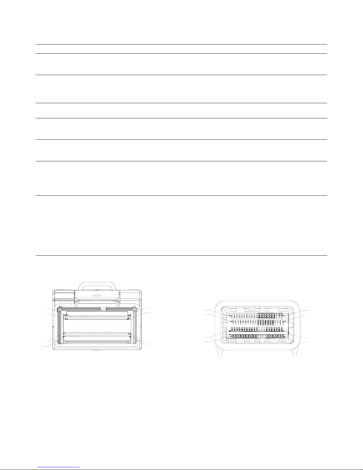
Pin Assignment
D1
C1
B1
A1
Figure 6. CXP module and host board connector pin assignments
D21
C21
B21
A21
D21
C21
B21
A21
D1
C1
B1
A1
10
Avago Technologies Condential
Page 11
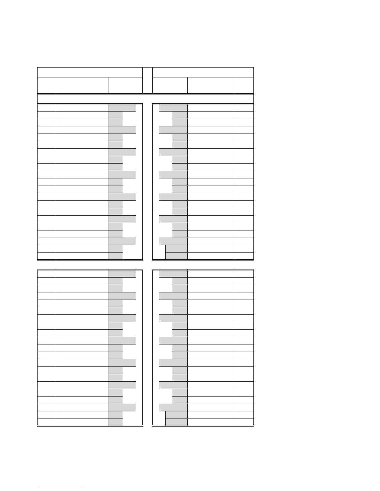
Transceiver Contact Assignment and Signal Description
There are 21 pads per level, for a total of 84, with 48 pads allocated for (12+12) dierential pairs, 28 for Signal Common
or Ground (GND), 4 for power connections, 4 for control/service.
Bottom side Top Side
I/O # Name
C1 GND
C2 Rx1p
C3 Rx1n
C4 GND
C5 Rx3p
C6 Rx3n
C7 GND
C8 Rx5p
C9 Rx5n
C10 GND
C11 Rx7p
C12 Rx7n
C13 GND
C14 Rx9p
C15 Rx9n
C16 GND
C17 Rx11p
C18 Rx11n
C19 GND
C20 PRSNT_L
C21 Int_L/Reset_L
A1 GND
A2 Tx1p
A3 Tx1n
A4 GND
A5 Tx3p
A6 Tx3n
A7 GND
A8 Tx5p
A9 Tx5n
A10 GND
A11 Tx7p
A12 Tx7n
A13 GND
A14 Tx9p
A15 Tx9n
A16 GND
A17 Tx11p
A18 Tx11n
A19 GND
A20 SCL
A21 SDA
Contact
Length
Receiver -- Top Card
Transmitter -- Bottom Card
Contact
Length
Card Edge
Card Edge
Name I/O #
GND D1
Rx0p D2
Rx0n D3
GND D4
Rx2p D5
Rx2n D6
GND D7
Rx4p D8
Rx4n D9
GND D10
Rx6p D11
Rx6n D12
GND D13
Rx8p D14
Rx8n D15
GND D16
Rx10p D17
Rx10n D18
GND D19
Vcc3.3-Rx D20
Not used D21
GND B1
Tx0p B2
Tx0n B3
GND B4
Tx2p B5
Tx2n B6
GND B7
Tx4p B8
Tx4n B9
GND B10
Tx6p B11
Tx6n B12
GND B13
Tx8p B14
Tx8n B15
GND B16
Tx10p B17
Tx10n B18
GND B19
Vcc3.3-Tx B20
Not used B21
11
Avago Technologies Condential
Page 12

Pin Signal Name Signal Description Logic Notes
A1 GND Ground
A2 TX1p Transmitter Non-Inverted Data Input CML-I
A3 TX1n Transmitter Inverted Data Input CML-I
A4 GND Ground
A5 TX3p Transmitter Non-Inverted Data Input CML-I
A6 TX3n Transmitter Inverted Data Input CML-I
A7 GND Ground
A8 TX5p Transmitter Non-Inverted Data Input CML-I
A9 TX5n Transmitter Inverted Data Input CML-I
A10 GND Ground
A11 TX7p Transmitter Non-Inverted Data Input CML-I
A12 TX7n Transmitter Inverted Data Input CML-I
A13 GND Ground
A14 TX9p Transmitter Non-Inverted Data Input CML-I
A15 TX9n Transmitter Inverted Data Input CML-I
A16 GND Ground
A17 TX11p Transmitter Non-Inverted Data Input CML-I
A18 TX11n Transmitter Inverted Data Input CML-I
A19 GND Ground
A20 SCL Two-wire serial interface clock LVCMOS-I/O 1
A21 SDA Two-wire serial interface data LVCMOS-I/O 1
B1 GND Ground
B2 TX0p Transmitter Non-Inverted Data Input CML-I
B3 TX0n Transmitter Inverted Data Input CML-I
B4 GND Ground
B5 TX2p Transmitter Non-Inverted Data Input CML-I
B6 TX2n Transmitter Inverted Data Input CML-I
B7 GND Ground
B8 TX4p Transmitter Non-Inverted Data Input CML-I
B9 TX4n Transmitter Inverted Data Input CML-I
B10 GND Ground
B11 TX6p Transmitter Non-Inverted Data Input CML-I
B12 TX6n Transmitter Inverted Data Input CML-I
B13 GND Ground
B14 TX8p Transmitter Non-Inverted Data Input CML-I
B15 TX8n Transmitter Inverted Data Input CML-I
B16 GND Ground
B17 TX10p Transmitter Non-Inverted Data Input CML-I
B18 TX10n Transmitter Inverted Data Input CML-I
B19 GND Ground
B20 VCC3.3-TX +3.3 V Power supply Transmitter
B21 Not used Not used , 3.3 V only
Note:
1. Host shall use a pull up of 1.5 kohm – 10 kohm to Vcc3.3.
12
Avago Technologies Condential
Page 13

Pin Signal Name Signal Description Logic Notes
C1 GND Ground
C2 RX1p Receiver Non-Inverted Data Output CML-O
C3 RX1n Receiver Inverted Data Output CML-O
C4 GND Ground
C5 RX3p Receiver Non-Inverted Data Output CML-O
C6 RX3n Receiver Inverted Data Output CML-O
C7 GND Ground
C8 RX5p Receiver Non-Inverted Data Output CML-O
C9 RX5n Receiver Inverted Data Output CML-O
C10 GND Ground
C11 RX7p Receiver Non-Inverted Data Output CML-O
C12 RX7n Receiver Inverted Data Output CML-O
C13 GND Ground
C14 RX9p Receiver Non-Inverted Data Output CML-O
C15 RX9n Receiver Inverted Data Output CML-O
C16 GND Ground
C17 RX11p Receiver Non-Inverted Data Output CML-O
C18 RX11n Receiver Inverted Data Output CML-O
C19 GND Ground
C20 PRSNT_L Module Present O 1
C21 Int_L/Reset_L Interrupt / Reset I/O 2
D1 GND Ground
D2 RX0p Receiver Non-Inverted Data Output CML-O
D3 RX0n Receiver Inverted Data Output CML-O
D4 GND Ground
D5 RX2p Receiver Non-Inverted Data Output CML-O
D6 RX2n Receiver Inverted Data Output CML-O
D7 GND Ground
D8 RX4p Receiver Non-Inverted Data Output CML-O
D9 RX4n Receiver Inverted Data Output CML-O
D10 GND Ground
D11 RX6p Receiver Non-Inverted Data Output CML-O
D12 RX6n Receiver Inverted Data Output CML-O
D13 GND Ground
D14 RX8p Receiver Non-Inverted Data Output CML-O
D15 RX8n Receiver Inverted Data Output CML-O
D16 GND Ground
D17 RX10p Receiver Non-Inverted Data Output CML-O
D18 RX10n Receiver Inverted Data Output CML-O
D19 GND Ground
D20 VCC3.3-RX +3.3 V Power supply receiver
D21 Not used Not used , 3.3 V only
Notes:
1. Shorted directly to GND inside the module.
2. Int_L/Reset_L is a bidirectional contact. When driven from the host, it operates logically as a Reset signal (input). When driven from the module, it
operates logically as an Interrupt signal (output). Signal levels are per specied in Low Speed Logic section. Host shall use a pull up of 1.5 kohm – 10
kohm to Vcc3.3 for this pin.
13
Avago Technologies Condential
Page 14

Control Interface
Int_L operation:
The control interface includes a bi-directional Int_L/
Reset_L interrupt/reset signal and two-wire serial – SCL
(clock) and SDA (data) signals to provide users rich functionality over an ecient and easily used interface. The
TWS interface is implemented as a slave device and compatible with industry standard two-wire serial protocol.
Signal and timing characteristics are further dened in
this section. In general, TWS bus timing and protocols
follow the implementation popularized in Atmel Two-wire
Serial EEPROMs.
Low-Speed Electrical Contact Denitions
SDA, SCL
SCL is the clock of the two-wire serial interface, and SDA is
the data for the two-wire interface. SCL and SDA must be
pulled up in the host through a pull-up resistor of value
appropriate to the overall bus capacitance and the rise
and fall time requirements as per “CXP two-wire Serial
Interface Timing Specications” table.
The host supplied SCL input to the CXP transceiver is used
to positive-edge clock data into each CXP device and negative-edge clock data out of each device. CXP transceivers
operate only as slave devices. The host must provide a bus
master for SCL and initiate all read/write communication.
Since all CXP transceivers use the same two base
addresses, each CXP port requires its own SCL/SDA bus.
Support of multiple ports in a host requires multiple SCL/
SDA buses, or multiplexing circuitry such as a multiplexer
chip or a switch chip.
INT_L/RESET_L
Int_L/Reset_L is a bidirectional contact. When driven
from the host, it op erates logically as a Reset signal.
When driven from the module, it oper ates logically as an
Interrupt signal. In both cases, the signal is asserted low,
as indicated by the ’_L’ sux. The Int_L/Reset_L signal
requires open collector outputs in both the host and
the module, and must be pulled up on the host board
with 1.5 kohm – 10 kohm resistor. The two uses are
distinguished by timing – a shorter assertion, driven by
the module indicates an interrupt and a longer assertion
of the signal driven by the host indicates a reset as per “I/O
Timing for Control and Status Functions” Table below.
When Int_L/Reset_L is pulled “Low” by the module for
longer than the minimum pulse width (t
shorter than the maximum pulse width (t
signal signies an interrupt. When asserted “Low”, Int_L
indicates a possible module operational fault or a status
critical to the host system. The host identies the cause
of the interrupt using the two-wire serial interface. Int_L
must operate in Pulse mode (as opposed to Static mode),
in order to distinguish a short Int_L signal from a longer
Reset_L signal, so the module must de-assert Int_L/
Reset_L after the interrupt has been signaled.
Int_L, PW-min
Int_L, PW-max
) and
) the
Reset_L operation:
When the Int_L/Reset_L signal is pulled “Low” by the
host for longer than the minimum reset pulse length
(t
Reset_L,PW-min
returning all user module settings to their default state.
There is no maximum reset pulse length. Module Reset
Assert Time (t_init) starts on the rising edge after the
low level on the Reset_L signal is released. During the
execution of a reset (t_init) the host shall disregard all
status bits until the module indicates a completion of the
reset interrupt. The module indicates this by posting an
Int_L signal with the Data_Not_Ready bit (Memory Map,
Byte 2, bit 0) negated. Note that on power up (including
hot insertion) the module will post this completion of
reset interrupt without requiring a reset from the host.
), it ini tiates a complete module reset,
PRSNT_L
PRSNT_L is used to indicate when the module it plugged
into the host re ceptacle. PRSNT_L is pulled up to Vcc3.3
on the host board through > 50 kW and pulled down
directly to signal common (no re sistor) in the module. The
PRSNT_L is asserted “Low” when inserted and deas serted
“High” when the module is physically absent from the host
con nector.
14
Avago Technologies Condential
Page 15

I/O Timing for Control and Status Functions
Parameter Symbol Min Max Unit Condition, and Notes
Initialization Time t
Reset Pulse Width - Min. t
Monitor Data Ready Time t
Reset Assert Time t
Int_L Assert Time t
Interrupt Pulse Width - Min t
Interrupt Pulse Width - Max t
Int_L Deassert Time t
Rx LOS Assert Time t
Tx Fault Assert Time t
Flag Assert Time t
Mask Assert Time t
Mask Deassert Time t
Select Change Time t
Notes:
1. Time from power on, hot plug or rising edge of reset until the module is fully functional.
2. Power on is dened as the instant when supply voltages reach and remain at or above the minimum level as specied in the power supply
specications.
3. Fully functional is dened as Int_L asserted due to Data Not Ready (Byte 2, bit 0) deasserted. The module should meet the optical and electrical
specications.
4. This is the minimum Reset_L pulse width required to reset a module. Assertion of Reset_L activates a complete module reset, i.e. module returns
to the factory default control settings. While Reset_L is low, the Tx and Rx outputs are disabled and the module does not response to the 2WS
serial interface.
5. Time from power on to Data Not Ready (Byte 2, bit 0) deasserted and Int_L asserted.
6. Time from rising edge on the Reset_L contact until the module is fully functional. During the Reset Time module will not respond to a “low” on the
Int_L/Reset_L signal.
7. Time from occurrence of condition triggering Int_L until Vout:Int_L = Vol.
8. Int_L operates in pulse mode. Static mode (Int_L stays low until reset by host) is not supported for Int_L.
9. Int_L pulse width must not exceed t
10. Time from clear on read operation of associated ag until Int_L Status (Lower page, byte 2, bit 1) is cleared. This includes deassert times for Rx LOS,
Tx Fault and other ag bit. Measured from falling clock edge after stop bit of read transaction.
11. Time from Rx LOS state to Rx LOS bit set (value = 1b) and Int_L asserted.
12. Time from Tx Fault state to Tx Fault bit set (value = 1b) and Int_L asserted.
13. Time from occurrence of condition triggering ag to associated ag bit set (value = 1b) and Int_L asserted.
14. Time from mask bit set (value = 1b) until associated Int_L assertion is inhibited.
15. Time from mask bit cleared (value = 0b) until associated Int_L operation resumes.
16. Time from change of state of Application or Rate Select bit until transmitter or receiver bandwidth is in conformance with appropriate specication.
Int_L,PW-max
init
reset_L,PW-min
data
RSTL,OFF
Int_L,ON
Int_L,PW-min
Int_L,PW-max
Int_L,OFF
LOS,ON
Txfault,ON
ag,ON
mask,OFF
mask,ON
ratesel
to distinguish Int_L from a Reset for other devices on bus.
25 ms Note 4
5
2000 ms Note 1 2, 3
2000 ms Note 5
2000 ms Note 6
200 ms Note 7
Note 8
Note 9
50
ms
ms
100 ms Note 10
100 ms Note 11
200 ms Note 12
200 ms Note 13
100 ms Note 14
100 ms Note 15
100 ms Note 16
15
Avago Technologies Condential
Page 16
Low Speed Logic
Management signaling logic levels are based on Low Voltage CMOS operating at 3.3 V Vcc. Host shall use a pull-up
(1.5 kohm – 10 kohm) to V
for the Two-wire interface SCL (clock), SDA (address & data), and Int_L/Reset_L signals.
cc3.3
Low Speed Control and Sense Signal Specications
Parameter Symbol Min Max Units Condition
Module Input Voltage Low V
Module Input Voltage High V
Module Output Voltage Low V
Module Output Voltage High V
Module Output Current High I
Capacitance of module on SCL, SDA
and Int_L/Reset_L I/O contacts
Capacitance of module on
Int_L/Reset_L I/O contact
Total bus capacitive load, SCL, SDA
and Int_L/Reset_L I/O pin
il
ih
ol
oh
oh
C
i,SCLSDA
C
i,INT_L
C
b
-0.3 0.4 V Pull-up to 3.3V.
2.3 3.6 V
Min Vih = 0.7*3.3V.
-0.3 0.3 V Condition IOL=3.0 mA. Pull-up to 3.3V.
2.8 3.6 V Min Voh = 3.3V - 0.5V.
-10 10
mA
-0.3 V < Voutput < 3.6 V
36 pF Allocate 28 pF for IC, 8 pF for module PCB
36 pF Allocate 28 pF for IC, 8 pF for module PCB
100 pF
200 pF
3.0 kW Pullup resistor, max
1.6 kW Pullup resistor, max
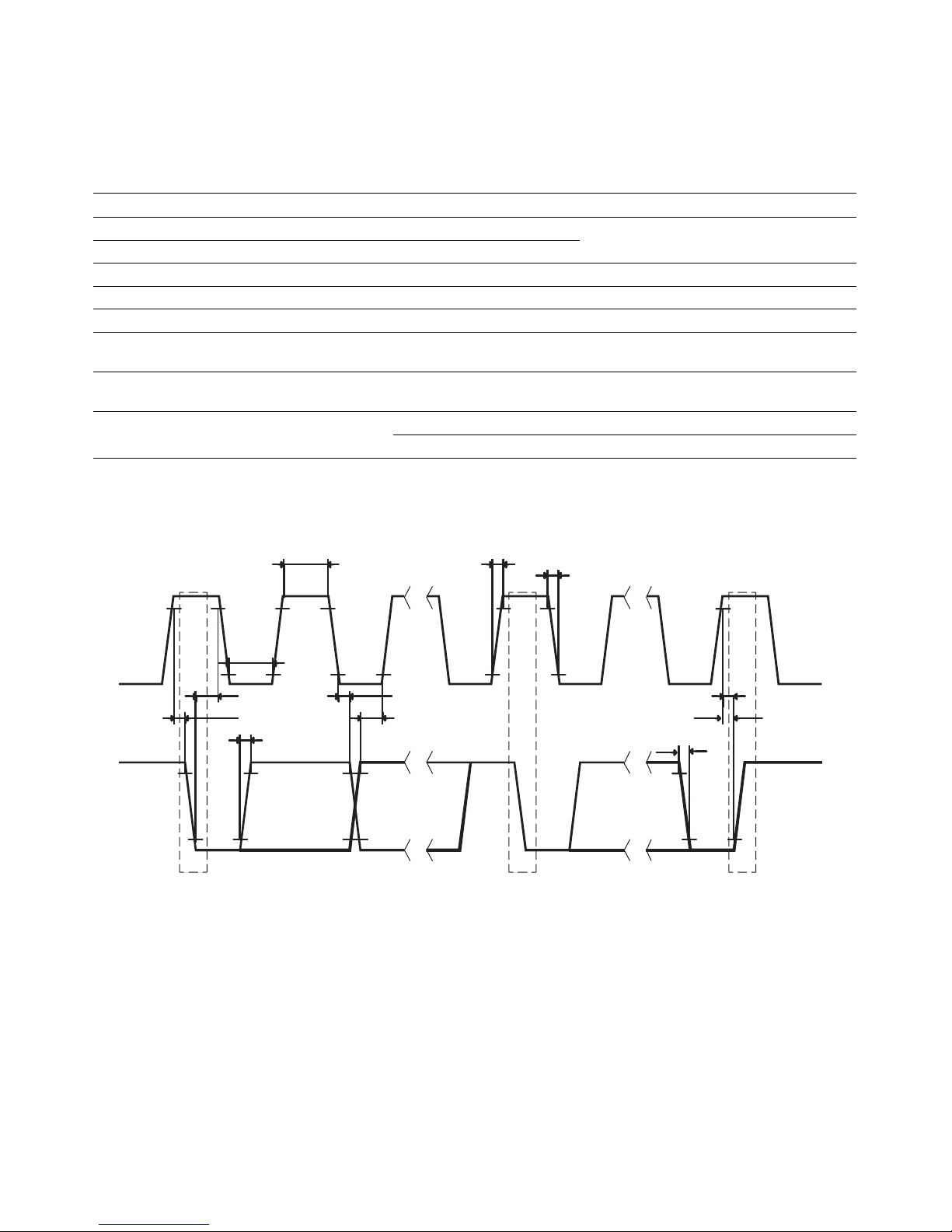
Management Interface Timing Specication
t
HIGH
SCL
t
LOW
t
HD,STA
t
SU,STA
t
R
SDA
Figure 7. Two-wire Serial Interface Timing Diagram
t
HD,DAT
t
SU,DAT
t
R
t
F
t
t
SU,STO
t
F
STOPReSTARTSTART
16
Avago Technologies Condential
Page 17

CXP Two-Wire Serial Interface Timing Specications
Parameter Symbol Min Max Unit Condition
Clock Frequency f
Clock Pulse Width Low t
Clock Pulse Width High t
Time bus free before new transmission can start t
START Set-up Time t
START Hold Time t
Data Set-up Time t
Data Hold Time t
SDA and SCL rise time t
SDA and SCL fall time t
STOP Set-up Time t
Notes:
1. Between STOP & START and between ACK & ReSTART.
2. Data In Set Up Time is measured from Vil(max)SDA or Vih(min)SDA to Vil(max)SCL.
3. Data In Hold Time is measured from Vil(max)SCL to Vil(max)SDA or Vih(min)SDA.
4. Rise Time is measured from Vol(max)SDA to Voh(min)SDA.
5. Fall Time is measured from Voh(min)SDA to Vol(max)SDA.
SCL
LOW
HIGH
BUF
SU,STA
HD,STA
SU,DAT
HD,DAT
R,400
F,400
SU,STO
0 400 kHz
1.3
0.6
20
0.6
0.6
0.1
0
0.3
0.3
0.6
ms
ms
ms
ms
ms
ms
ms
ms
ms
ms
Note 1
Note 2
Note 3
Note 4
Note 5
Memory Specications
Memory may be accessed in single-byte or multi-byte (up to 4 bytes) memory blocks. The largest multiple-byte contiguous write operation that a module shall handle is 4 bytes. The minimum size write block is 1 byte.
Memory Transaction Timing Specication
Parameter Symbol Min Max Unit Condition
Serial Interface Clock Holdo - “Clock Stretching” T_clock_hold 500
Complete Single or Sequential Write t
WR
40 ms Note 2
ms
Endurance (Write cycles) 50,000 75,000 cycles Note 3
Notes:
1. Maximum time the CXP module may hold the SCL line low before continuing with a read or write operation.
2. Complete up to 4 Byte write. Timing should start from Stop bit at the end of the sequential write operation and continue until the module responds
to another operation.
3. 50 K write cycles at 70°C.
Note 1
17
Avago Technologies Condential
Page 18

I/O Timing for Squelch and Disable
Parameter Symbol Min Max Unit Condition and Notes
Rx Squelch Assert Time t
Rx Squelch Deassert Time t
Tx Squelch Assert Time t
Tx Squelch Deassert Time t
Tx Disable Assert Time t
Tx Disable Deassert Time t
Rx Output Disable Assert Time t
Rx Output Disable Deassert Time t
Squelch Disable Assert Time t
Squelch Disable Deassert Time t
Notes:
1. Time from loss of Rx input signal until the squelched output condition is reached.
2. Time from resumption of Rx input signals until normal Rx output condition is reached.
3. Time from loss of Tx input signal until the squelched output condition is reached.
4. Time from resumption of Tx input signals until normal Tx output condition is reached.
5. Time from Tx Disable bit set (value = 1b) until optical output falls below 10% of nominal.
6. Time from Tx Disable bit cleared (value = 0b) until optical output rises above 90% of nominal. Measured from Stop bit low-to-high SDA transition.
7. Time from Rx Output Disable bit set (value = 1b) until Rx output falls below 10% of nominal.
8. Time from Rx Output Disable bit cleared (value = 0b) until Rx output rises above 90% of nominal.
9. This applies to Rx and Tx Squelch and is the time from bit set (value = 1b) until squelch functionality is disabled.
10. This applies to Rx and Tx Squelch and is the time from bit cleared (value = 0b) until squelch functionality is enabled.
Rxsq,ON
Rxsq,OFF
Txsq,ON
Txsq,OFF
Txdis,ON
Txdis,OFF
Rxdis,ON
Rxdis,OFF
Sqdis,ON
Sqdis,OFF
0.080 ms Note 1
0.080 ms Note 2
400 ms Note 3
400 ms Note 4
100 ms Note 5
400 ms Note 6
100 ms Note 7
100 ms Note 8
100 ms Note 9
100 ms Note 10
18
Avago Technologies Condential
Page 19
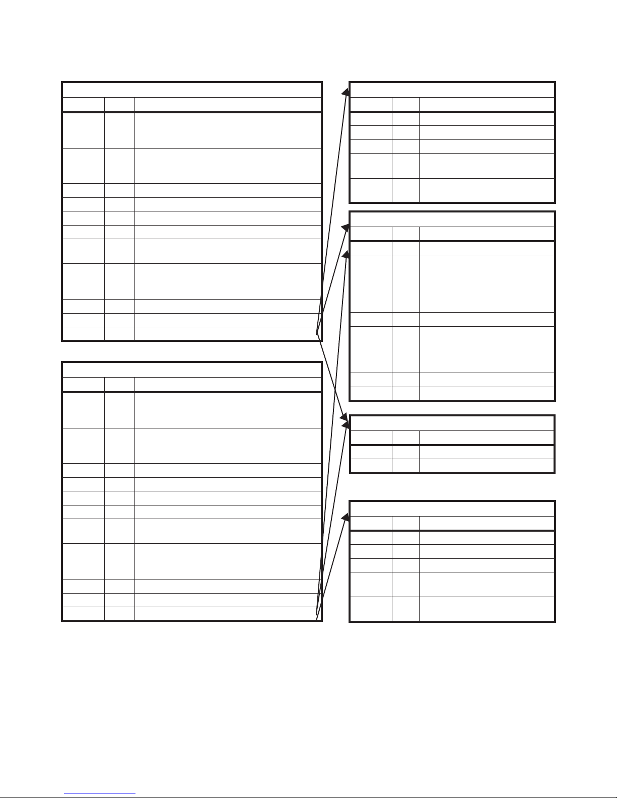
Memory Map
Tx Lower Page (1010 000x) – Required
Byte Type Functions
0-6 RO Tx Status: 0xA8 Presence, Flat/ Paging Memory
Presence, Interrupt, Data Not Ready, Loss of
Signal, Fault, Summary of Alarms
7-18 RO Latched Tx Alarms: Loss of Signal, Fault, Per-
channel Alarms (Power or Current High/Low),
Device Alarms (Temp, Vcc3.3 or Vcc12)
22-27 RO Module Monitors: Temp, Voltage
38-39 RO Module Monitors: Elapsed Operating Time
40-41 RW Module Control: Rate/Application Select
51 RW Module Control: Tx Reset
52-67 RW Tx Channel Control: Disables, Squelch, Polarity
Flip, Margin, Equalization Control
95-106 RW Masks for Alarms: Channel (LOS, Fault),
Channel Internal (Power or Current High/Low)
and Module (Temp, Voltage)
110-118 RW Vendor Specic Area – Read/Write
119-126 RW Password
127 RW Upper Page Select Byte (00h or 01h or 02h)
Rx Lower Page (1010 100x) – Optional
Byte Type Functions
0-6 RO Rx Status: Flat/ Paging Memory, Interrupt, Data
Not Ready, Loss of Signal, Fault, Summary of
Alarms
7-18 RO Latched Rx Alarms: Loss of Signal, Fault, Per-
channel Alarms (Power or Current High/Low),
Device Alarms (Temp, Vcc3.3 or Vcc12)
22-27 RO Module Monitors: Temp, Voltage
38-39 RO Module Monitors: Elapsed Operating Time
40-41 RW Module Control: Rate/Application Select
51 RW Module Control: Rx Reset
52-73 RW Rx Channel Control: Disables, Squelch, Polarity
Flip, Margin, Amplitude, Pre-emphasis Control
95-106 RW Masks for Alarms: Channel (LOS, Fault),
Channel Internal (Power High/Low) and
Module (Temp, Voltage)
110-118 RW Vendor Specic Area – Read/Write
119-126 RW Password
127 RW Upper Page Select Byte (00h or 01h or 02h)
Tx Upper Page 01h (Optional)
Byte Type Functions
128-167 RO Module Alarm Threshold Settings
168-179 RO Channel Alarm Threshold Settings
180-181 RO Checksum
182-229 RO Per-Channel Monitors: Tx Bias
Current and Light Output
230-255 Reserved – Vendor-Specic Tx
Functions
Upper Page 00h (identical for Tx & Rx) Required
Byte Type Functions
128-129 RO Identiers
130-146 RO Device Description: Cable & Con-
nector, Power Supplies, Max Case
Temp, Min-Max Signal Rate, Laser
Wavelength or Copper Attenua-
tion, and Supported Functions
147 RO Description: Device Technology
152-222 RO Vendor Information: Name &
OUI, PN & PN rev, Serial Number,
Data Code, & Customer-specic
Information
223 RO Checksum on 128-222
224-255 RO Vendor Specic Area – Read-only
Tx and/or Rx Upper Page 02h (Optional)
Byte Type Functions
128-247 RW User Writable EEPROM (120 B)
248-255 Reserved - Vendor Specic (8 B)
Rx Upper Page 01h (Optional)
Byte Type Functions
128-167 RO Module Alarm Threshold Settings
168-179 RO Channel Alarm Threshold Settings
180-181 RO Checksum
206-229 RO Per-Channel Monitors: Rx Input
Power
230-255 Reserved – Vendor-Specic Rx
Functions
19
Avago Technologies Condential
Page 20
Connector Orientation for 24 ber MTP/MPO connector
Fiber 12
Rx11
Fiber 24
Tx11
Figure 8. 24-ber MPO Receptacle
Fiber 1
Rx0
Fiber 13
Tx0
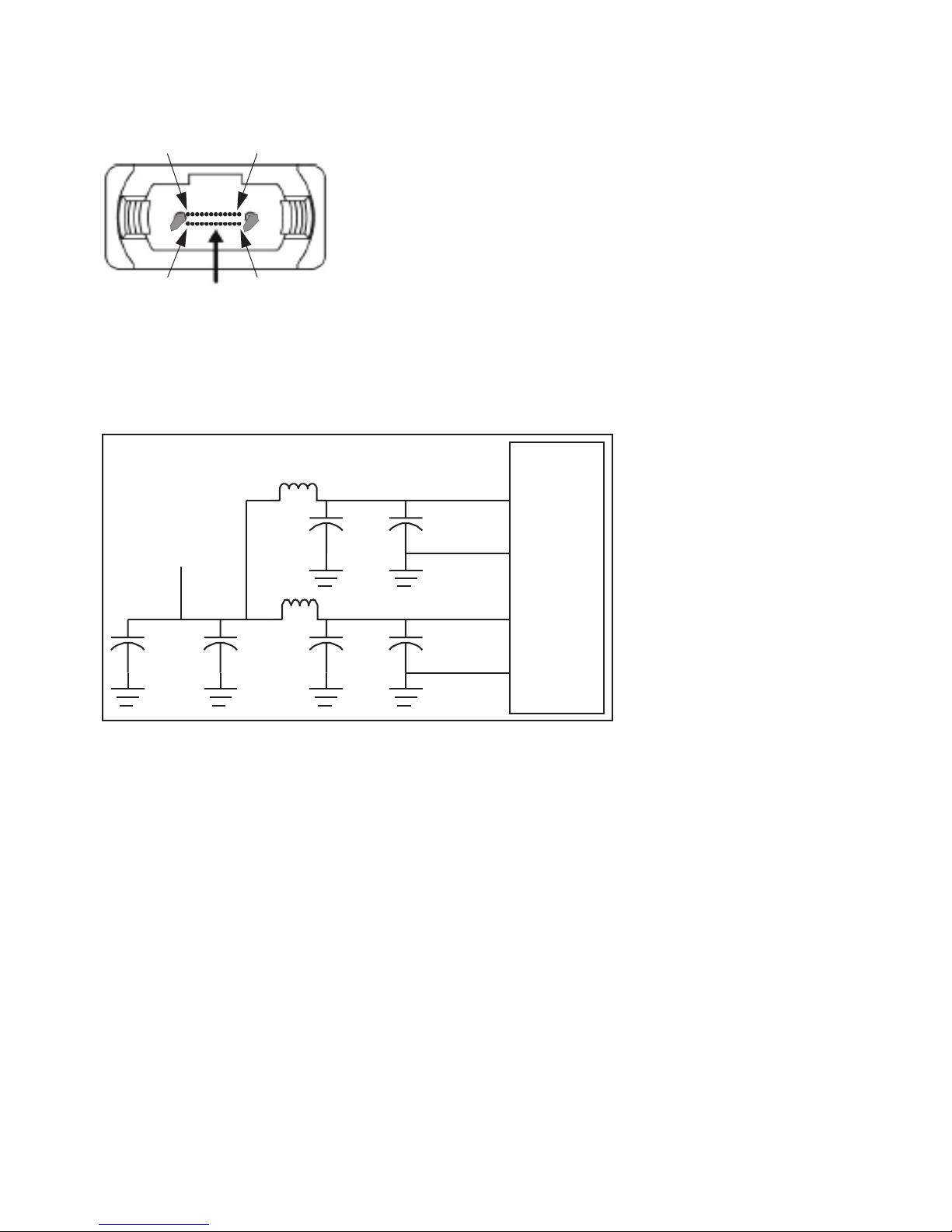
Recommended Power Supply Filter
Optical cables with 24-ber MPO-style connectors on each
end shall be built “Key up/Key down” so that the helix halftwist incurred when the cable is lugged into transceivers
will correctly connect transmitter lanes to receiver lanes:
lanes 0 to 0 and 11 to 11. MPO-style ‘male” alignment
pins are used in the receptacle and a “female” MPO-style
connector shall be used on the cable connector.
1 µH
Vcc_host = 3.3 V
1 µH
Figure 9. Recommended Power Supply Filter
10 µF
0.1 µF
0.1 µF 10 µF 0.1 µF 10 µF
CXP Module
Vcc3.3-Rx
GND
Vcc3.3-Tx
GND
20
Avago Technologies Condential
Page 21
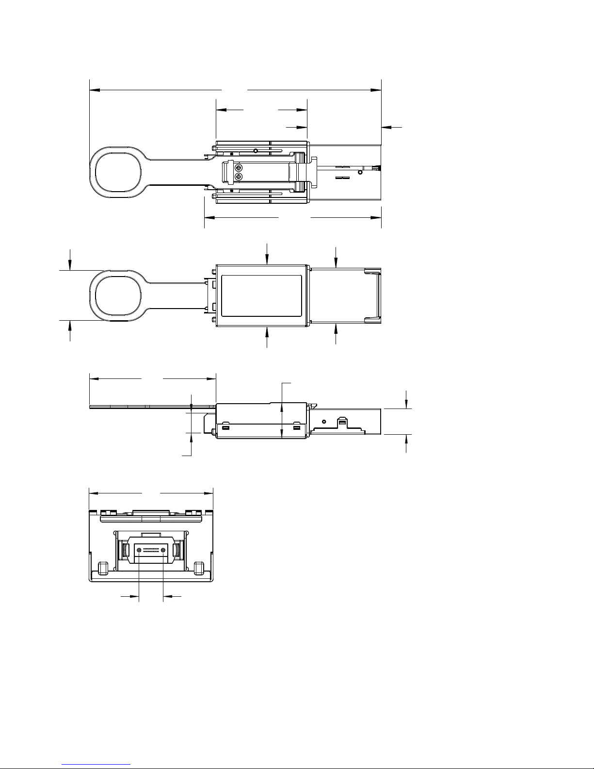
Mechanical Dimensions, Package Outline
112
34.93
28.45
67.92
19.21
48.62
23.9
7.69
23.9
21.2
13.73
9.81
4.6
All dimensions in millimeters
Figure 10. Transceiver package dimensions
21
Avago Technologies Condential
Page 22
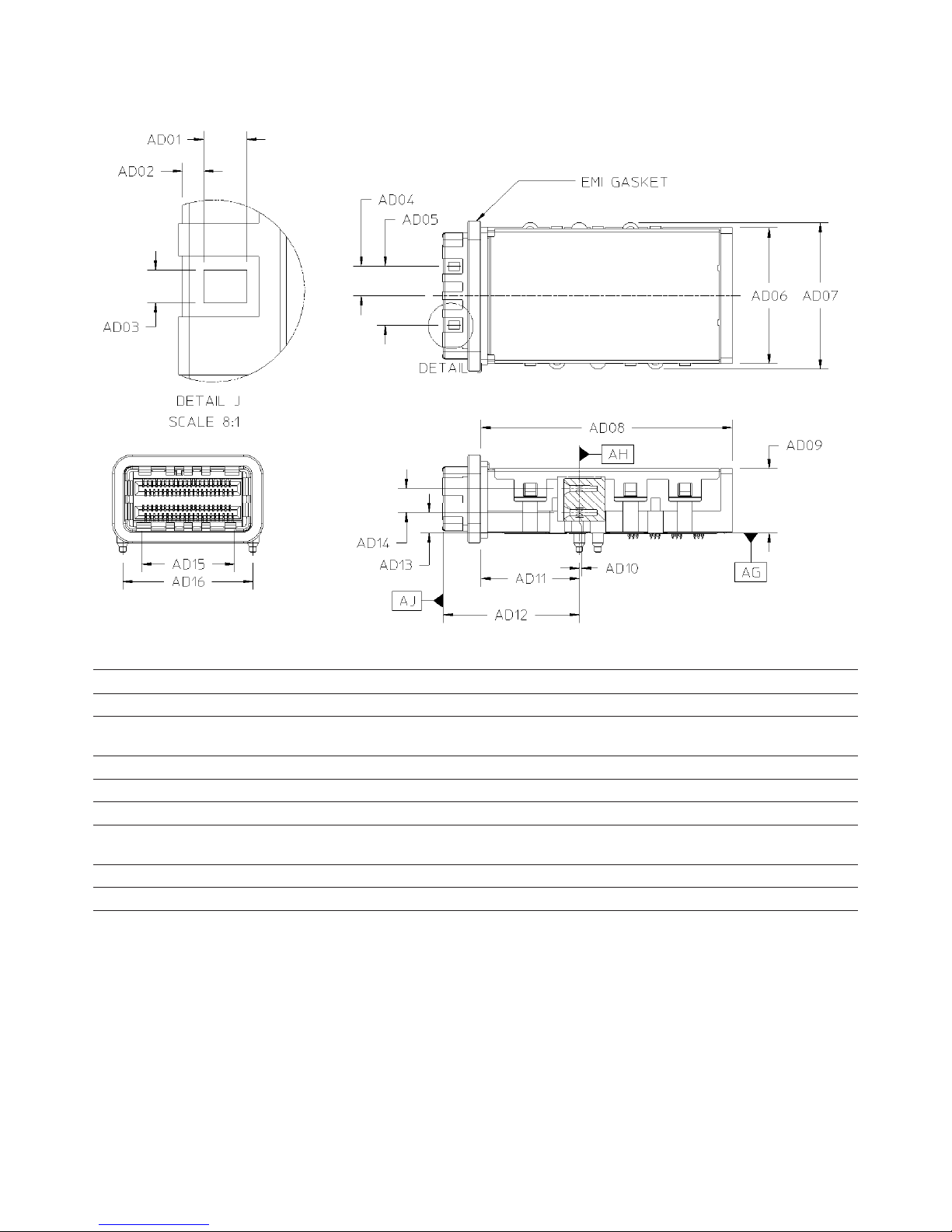
Host Board Connector
Figure 11. CXP host board connector dimensions (part 1 of 2)
ID Description Dim. Tol. (±) ID Description Dim. Tol. (±)
AD01 Latch Hole Length 2.00 0.10 AD09 Shell Height 11.88 0.13
AD02 Latch Hole from Face 0.97 0.05 AD10 Locating Post Centerline to Center-
line of Receptacle Co
AD03 Latch Hole Width 1.50 0.10 AD11 Locating Post to EMI Shell Base 18.06 0.13
AD04 Datum to Latch Hole 5.40 0.10 AD12 Locating Post to Face 25.06 0.08
AD05 Latch Hole to Hole 10.80 0.05 AD13 PCB to Lower Card Slot Centerline 3.75 0.10
AD06 Shell Width 25.05 0.25 AD14 Lower Card Slot to Upper Card Slot
Centerline
AD07 Shell Width at screw attach features 27.00 0.25 AD15 Card Slot Rib to Rib 17.18 0.10
AD08 EMI Shell Base to Back 46.22 0.25 AD16 Peg Centerline to Peg Centerline 24.00 0.08
0.05 0.05
4.50 0.10
22
Avago Technologies Condential
Page 23
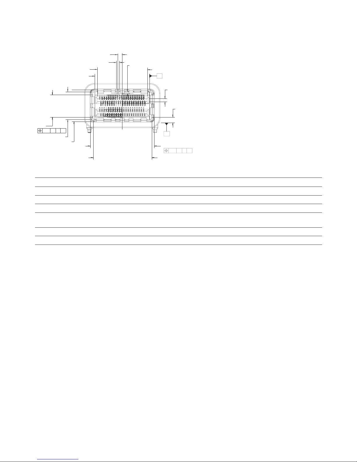
Host Board Connector (con't)
AE01
AE12
AE11
AE10
AE09
0.10 AG AH AK
AE08
AE07
Figure 12. CXP host board connector dimensions (part 2 of 2)
ID Description Dim. Tol. (±) ID Description Dim. Tol. (±)
AE01 Orientation Key Location 1.63 0.13 AE07 Snout Height 11.70 0.08
AE02 Orientation Key Location, Depth 20.75 Basic AE08 Snout Opening Height 10.20 0.05
AE03 Card Slot Height 1.18 0.05 AE09 Receptacle Body Height 8.00 0.08
AE04 Datum to Bottom of Receptacle
Housing
AE05 Snout Opening Width 21.60 0.05 AE11 Card Slot Width 18.20 0.05
AE06 Snout Width 23.10 0.08 AE12 Orientation Key Width 1.25 0.13
AE02
AK
AE03
AE04
AG
AE06
0.10 AG AH AK
AE05
2.09 0.10 AE10 Receptacle Body Width 19.94 0.08
23
Avago Technologies Condential
Page 24
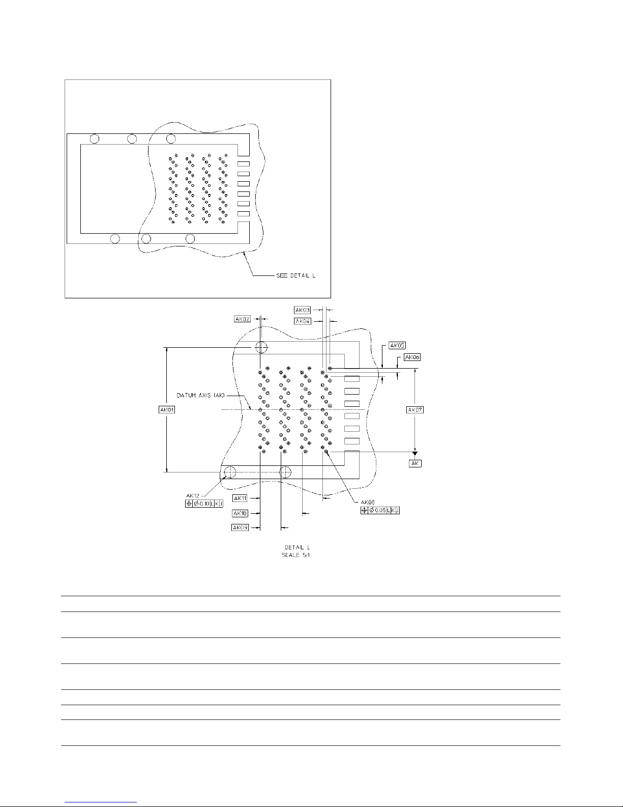
Host PCB Footprint
Figure 13. CXP host board connector footprint
ID Description Dim. Tol. (±) ID Description Dim. Tol. (±)
AK01 Locating Hole to Locating Hole 24.00 0.05 AK07 First to Last Column 16.00 Basic
AK02 Locating Hole to First Row of Signal
Holes
AK03 First Row to Second Row of Signal
Holes
AK04 First Row to Third Row of Signal Holes 1.40 Basic AK10 Row A to Row C 8.00 Basic
AK05 Column to Column Pitch 1.60 Basic AK11 Row A to Row D 12.00 Basic
AK06 Column to Column Pitch 0.80 Basic AK12 Locating Hole Diameter (Finished
24
0.20 Basic AK08 Contact Hole Diameter (Finished
PTH)
0.70 Basic AK09 Row A to Row B 4.00 Basic
PTH)
0.37 0.05
2.20 0.05
Avago Technologies Condential
Page 25
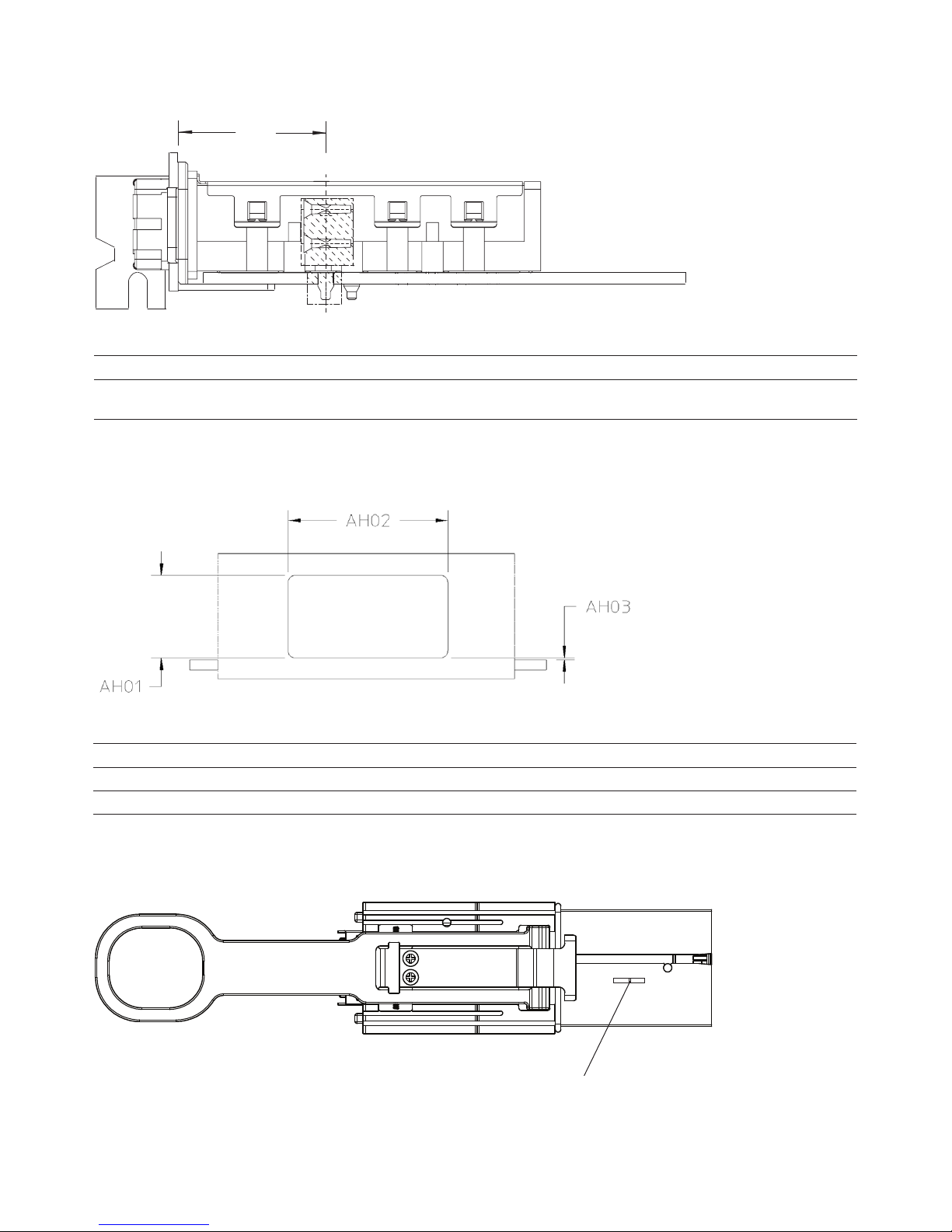
CXP Cage and Bezel
AJ01
Figure 14. CXP cage-to-bezel dimensions
ID Description Dim. Tol. (±) ID Description Dim. Tol. (±)
AJ01 Centerline of Receptacle Contacts to
Base of EMI Shell
19.66 Basic AJ02 - - -
Bezel Opening
Figure 15. CXP bezel opening dimensions
ID Description Dim. Tol. (±) ID Description Dim. Tol. (±)
AH01 Cutout Height 12.10 Basic AH03 Bottom of Cutout to Peg 0.28 Basic
AH02 Cutout Length 23.50 Basic AH04 - - -
Heat Sink interface and Case Temperature Measurement point on the Connector Plug
Case Temperature Measurement Point
Figure 16. Case Temperature Measurement point
25
Avago Technologies Condential
Page 26

Insertion, Extraction and Retention Forces for the CXP Transceiver
Symbol Parameter Min Max Unit Comments
F
i
F
w
F
r
F
rcl
F
rhb
N
hc
N
x
CXP module insertion force 150 N EIA 364-13
CXP module extraction 50 N EIA 364-13
CXP module retention 90 170 N Load pull, per EIA 364-38A
No damage to transceiver below 90N
Cage retention (latch strength) 180 N No damage to latch below 180N
Cage retention in host board 114 N Force to be applied in a vertical direction,
no damage to cage
Insertion / removal cycles,
connector/receptacle
Insertion / removal cycles,
100 Cycles Number of cycles for the connector and
receptacle with multiple transceivers
50 Cycles Number of cycles for an individual module
CXP module
For product information and a complete list of distributors, please go to our web site: www.avagotech.com
Avago, Avago Technologies, and the A logo are trademarks of Avago Technologies in the United States and other countries.
Data subject to change. Copyright © 2005-2013 Avago Technologies. All rights reserved.
AV02-3753EN - February 15, 2013
Avago Technologies Condential
Avago Technologies Condential
 Loading...