

Page 1
VERSION 1.9
J120 (38198-X)
J120
technical reference manual
38198-X
Version 1.9
Preliminary
March 2018
Auvidea GmbH
Kellerberg 3
D-86920 Denklingen
Te l: +49 824 3 77 1 4 6 2 2
[email protected]
www.auvidea.com!
AUVIDEA GMBH
TECHNICAL REFERENCE MANUAL
1
Page 2

VERSION 1.9
J120 (38198-X)
Copyright Notice
Trad em ar ks
NVIDIA, the NVIDIA logo, CUDA, Jetson, Maxwell,Tegra and VisionWorks are registered trademarks and/or
trademarks of NVIDIA Corporation in the United States and!other countries. Other company and product names
may be trademarks of the respective companies with which they are associated.
© Auvidea GmbH 2016
All Rights Reserved
No part of this document or any of its contents may be reproduced, copied, modified or adapted, without the
prior written consent of the author, unless otherwise indicated for stand-alone materials.
You may share this document by any of the following means: this PDF file may be distributed freely, as long as
no changes or modifications to the document are made.
For any other mode of sharing, please contact the author at the email below. [email protected]
Commercial use and distribution of the contents of this document is not allowed without express and prior
written consent of Auvidea GmbH.
AUVIDEA GMBH
TECHNICAL REFERENCE MANUAL
2
Page 3
VERSION 1.9
J120 (38198-X)
Features
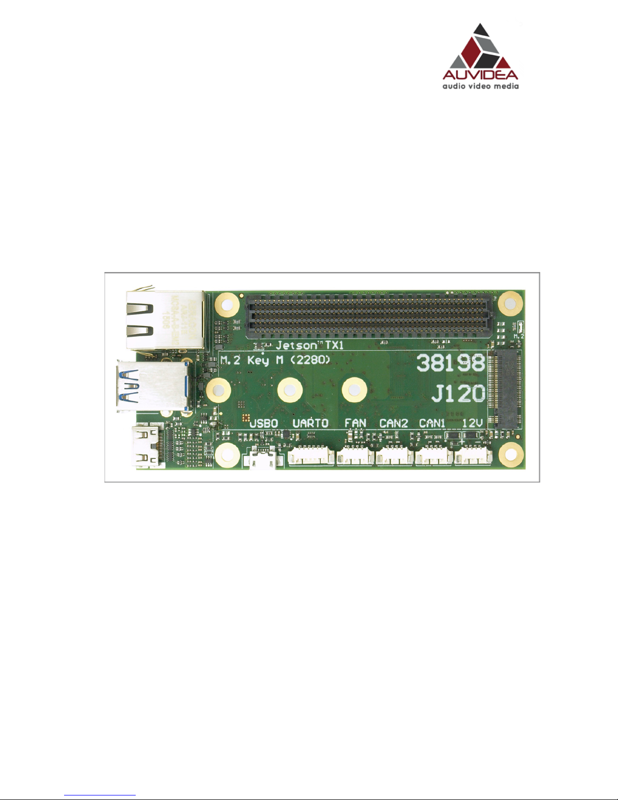
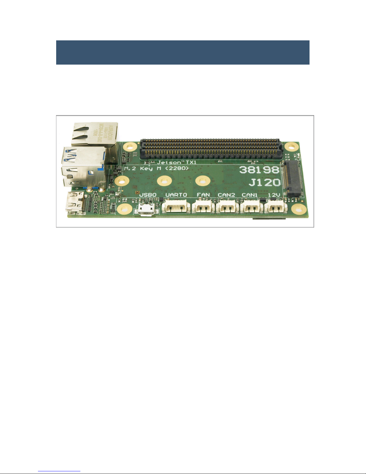
J120 carrier board for the NVIDIA® Jetson™ TX1
The J120 carrier board is slightly larger than the TX1 compute module. It has the same height but it extends
out to to the left side, to make room for the USB3 and RJ45 connectors. It is plugged in below the TX1 and
brings out many interfaces on connectors.
Techn ical de tai ls
• carrier board for one NVIDIA® Jetson™ TX1 compute module
• standalone operation
• one 4 lane CSI-2 (22 pin FPC 0.5mm pitch) - B102
• micro SD card
• two USB3 type A
• RJ45 connector for 10/100/1000BT Ethernet
• UART 0 (3.3V TTL) (6 pin) - console access
• one I2S digital audio (6 pins each)
• fan connector (4 pin)
• mini HDMI out
• M.2 type M 2280 (not operational on J120 rev 1)
• size: 50 x 119 mm (size of the PCB)
• height: 16 mm (incl. TX1 without heatsink without height of bottom side components of J100)
• height: 21 mm (incl. TX1 without heatsink including height of bottom side components of J100)
• weight: 42 grams (just the J120)
• TX1 weight: 144 grams (TX1 with heatsink), 75 grams (TX1 w/o heatsink)
• mounting: 4 M3 holes with 3.2mm each (42 x 79 mm spacing - 4 mm from each edge)
• model: 38198 (J120 rev 1)
Power
• power: 12V typical (4 pin) - 2 power pins for redundant powering
• range: 7V to 17V
• do not use the 19V power supply of the Jetson TX1 dev kit - it will damage the J120 carrier board
AUVIDEA GMBH
TECHNICAL REFERENCE MANUAL
3
Page 4

VERSION 1.9
J120 (38198-X)
How do the various models differ?
J100 + M100 (or M110)
The J100 may be plugged into the M100 motherboard. Three motherboard connectors carry signals for CAN,
Ethernet, UART, power, PCIe, SATA, SPI, I2C and more. The M110 features standard connectors for SATA and
PCIe (4 lanes).!
AUVIDEA GMBH
TECHNICAL REFERENCE MANUAL
4
Feature
J100
J100 + M100
J120
J130
J140
Jetson TX1 compatible
✓✓✓✓✓
HDMI out
mini
mini
mini
standard
mini
USB 3.0 type A
--242
micro USB 3.0
22-1-
micro USB 2.0 OTG
-
✓✓✓
✓
Wifi (2 antennas) on TX1
module
✓✓✓v✓
10/100/1000 Ethernet
(RJ45)
-1112
(TX1 + i210)
IMU MPU-9250 (optional 9
axis sensor)
✓✓✓✓✓
CAN controllers
-1111
SATA-M.2 B 2242
-
standard
standard
4x PCIe--
M.2 M 2280
PCIe slot
M.2 2280
micro SD card
✓✓✓✓✓
SPI/I2C--
1/1
UART1222
2
CSI-2 (22 pin - 4 lanes)
221
2 HDMI in
3
CSI-2 (15 pin - 2 lanes)
22---
I2S (digital audio)
2
2
1 (2 channels)
2 HDMI in
1 (8 channels)
fan connector
✓✓✓✓✓
switches: power, reset,
force recovery
-
✓✓✓
✓
size
50x87mm
98x87mm
50x110mm
74x110mm
68x110mm
power in
7 .. 17V
7..42V
7 .. 17V
7 .. 17V
7 .. 17V
battery charger & backup
----2S Lipo
Page 5

VERSION 1.9
J120 (38198-X)
J120 Rev 1 (38198)
First revision of the J120. Very limited distribution.
J120 Rev 2 (38198-2)
Second revision of the J120. It became available in late April 2016. Modifications:
• all 3 connectors on the left are aligned (Ethernet, USB3 and mini HDMI)
• PCB size: 50 x 109.5 mm, total size: 50 x 110 mm
• M.2 type M fixed
• auto start recovery time shortened
• optional super cap for RTC
• firmware upgrade (back powering fix)
• INT lines of CAN controllers connect to individual pins of the TX1 (interrupts not shared)
J120 Rev 3 (38198-3)
• fixed USB2 power (flash recovery now supported)
• optional resistor to combine power to the 2 USB 3 ports
• added UART2 RXD/TXD to J7 (with components changes it could be reverted back to UART0 RTS/CTS)
• replaced 12V power in diodes with MOSFETs (for controlled inrush ramp up with Lipo batteries)
• four TX1 mount holes now connected to GND
• added LM75 temp sensor
• only one CAN bus and connector (CAN2) to overcome problem with SPI1_CS0 line - one CAN bus
supported with TX1 firmware provided by Auvidea
J120 Rev 4 (38198-4)
• changed I2C pullup resistors from 1k to 10k (to improve I2C signal low level)
J120 Rev 5 (38198-5)
• I2S connector: changed from I2S2 to I2S0 (for additional GPIOs)
• optional: 2 CAN busses (requires SW fix for SPI1_CS0)
• M.3 spacer to fix M.2 2280 SSD card
• bottom USB3 connector may be configured to carry SATA signals (optional)
J120 Rev 6 (38198-6)
• added MCU (STM32F042) for watchdog option - this MCU tunnels the UART0 port of the TX1 and TX2
• initial revs of the MCU firmware only support 38400 baud
• added INA3221 power monitor chip (12V, 5V, 3.3V) - this chip is not populated on the base version
J120 Rev 7 (38198-7)
• RN45 populated to bring out UART2 on connector J7
AUVIDEA GMBH
TECHNICAL REFERENCE MANUAL
5
Page 6
VERSION 1.9
J120 (38198-X)
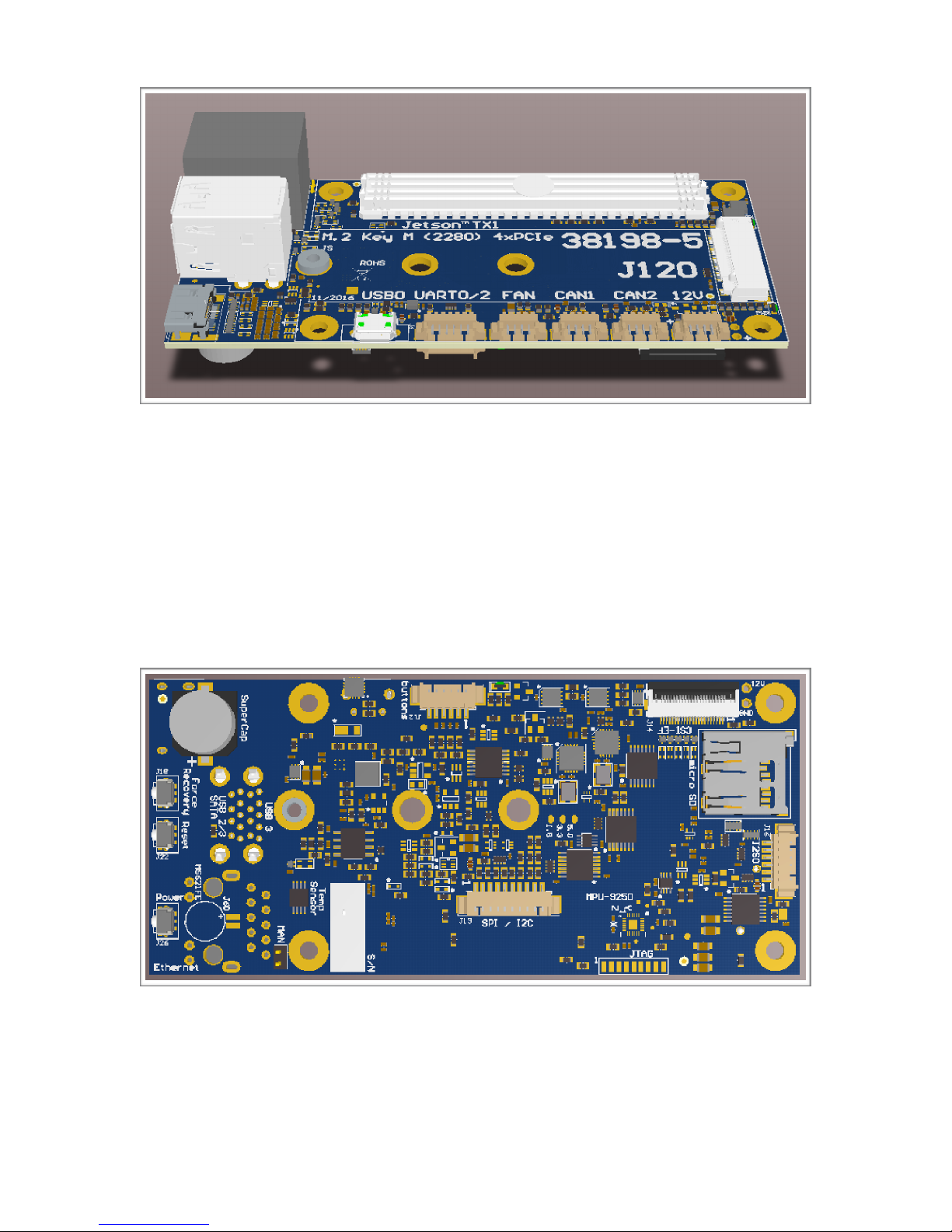
J120 rev 5 top side
J120 rev 5 bottom side
AUVIDEA GMBH
TECHNICAL REFERENCE MANUAL
6
Page 7

VERSION 1.9
J120 (38198-X)
The optional super cap is the tallest component on the bottom side (5.5mm high). The capacity of the super
cap is 47mF. Optionally the RTC (realtime clock of the Jetson TX1) may be powered by a Lithium cell
(MS621FE-FL11E). It is located next to the power button. If the super cap and the Lithium cell are not
populated, RTC power may be provided on the buttons connector (J12 pin 1).
Testing of the J120
The following functions are tested:
• HDMI out
• 1000BT Ethernet
• USB 3.0 on USB1
• USB 2.0 on USB2 (USB 3 mode requires modification of device tree file)
• micro SD card
• power consumption with 12 V power supply (Ubuntu booted and system idle)
Rev 3 and newer:
• CSI-2 interface with B102 HDMI to CSI-2 module
• CAN bus (communicating with Autoquad flight controller)
• IMU (with qtcreator test program)
• M.2 2280 PCIe SSD
Please have a look at the test report which is included with the shipment.
STEP (3D) models
J120 rev 1: http://www.auvidea.eu/download/step/38198.step.zip
J120 rev 2: http://www.auvidea.eu/download/step/38198-2.step.zip
AUVIDEA GMBH
TECHNICAL REFERENCE MANUAL
7
Page 8
VERSION 1.9
J120 (38198-X)
Getting started
Applying power
The J120 is powered by the on-board power connector (J11). Rev 1 and 2:
each of the 2 separate power pins features a Schottky diode. These 2 diodes
OR the 2 power inputs together. So 2 independent power inputs are provided
to achieve redundant powering. Rev 3+: reverse voltage protection and
inrush current limiting have been added (now single power input on 2 pins).
Alternatively the power wires may be soldered directly to the J120. Two
power holes have been added between the power connector and the mount
hole.
Auto start
The J120 automatically powers up the TX1 with a digital one shot which pulls
the POWER-BTN input of the TX1 low for approximately 1 second after power
is applied. When the TX1 raises the CARRIER_PWR (A48) line, the power
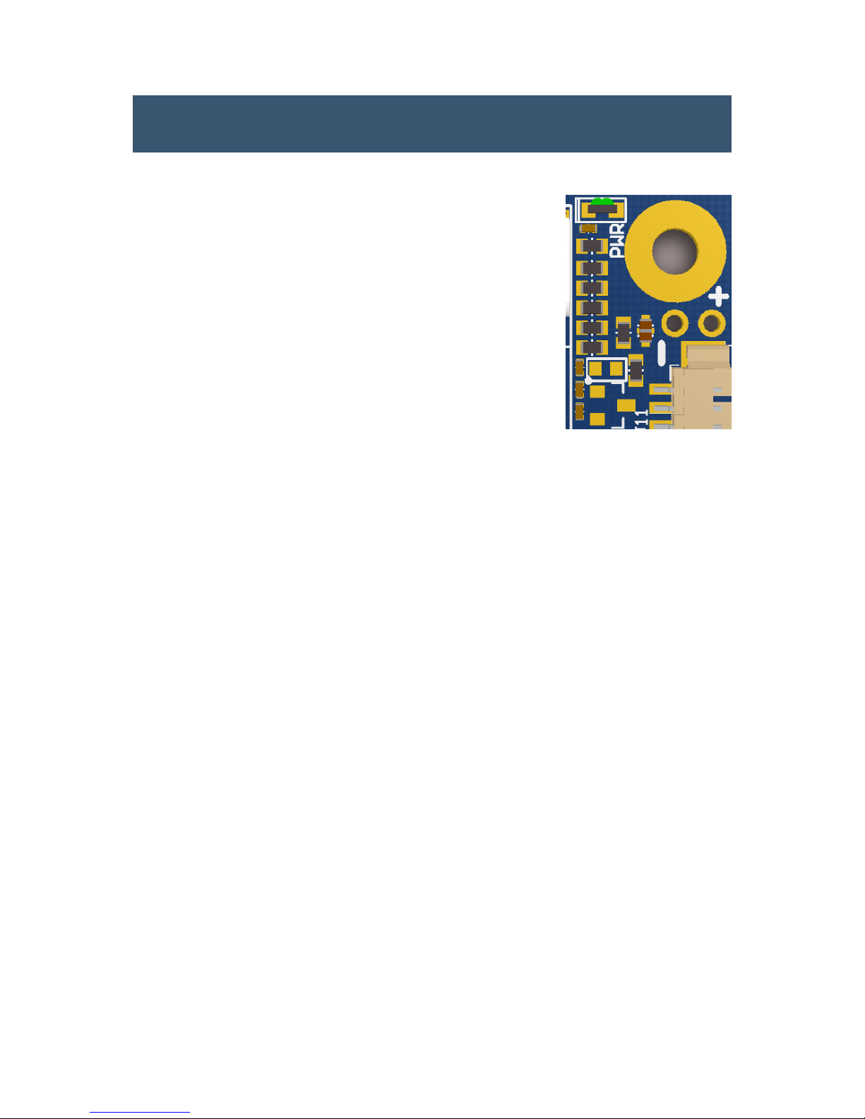
supplies on the J120 are powered up. This is indicated by lighting up the
green power LED below the fan connector. With rev 3 this LED moved to the
right of the M.2 connector.
The auto start logic is powered by Vdd_RTC (A50). Rev 1: for auto start to work, please power down the TX1
for at least 10 seconds. This allows time for the Vdd_RTC supply to drain and the enable auto start, when
power is applied again. Rev 2 of the J120 will shorten this time, by actively draining Vdd_RTC when the main
power is removed. Alternatively power up the J120 by pressing the power button. With rev 3 the auto start
logic is powered by the 12V power supply, not to drain Vdd_RTC and the super cap charge.
Console access
The console port of the TX1 is UART 0. The J120 converts this UART port to standard 3.3V TTL levels. So a
standard USB to TTL serial converter may be used to connect to the console. Just connect TXD, RXD and GND
to the USB converter. Make sure that you connect TXD to the RXD input of the USB TTL converter. Standard
baud rate it 115200. Settings: 8/1/N.
Firmware upgrade of the TX1
The J120 does support a direct firmware upgrade of the TX1. However, there is one issue on rev 1. Once the
USB cable to USB0 is connected the J120 will be back powered through USB. In this mode the J120 will not
boot. Please put the the TX1 into the upgrade mode with the recovery button before connecting the USB cable
to USB0. Alternatively please perform the firmware upgrade on the TX1 development board. Firmware upgrade
is supported fine on the newer revs.
AUVIDEA GMBH
TECHNICAL REFERENCE MANUAL
8
Page 9
VERSION 1.9
J120 (38198-X)
CSI-2 video in
CSI-2 connector
The J120 features one CSI-2 connector with 4 data lanes. It is a 22 pin FPC connector with 0.5mm pitch. It has
the same pin out as the 22 pin CSI-2 connector found on the carrier board for the Raspberry Pi compute
module. Support for the Raspberry Pi cameras is planned.
B102
The B102 is an HDMI to CSI-2 converter module, which may directly be connected to the CSI-2 connector of the
J120. It provides raw uncompressed video to the Jetson TX1 with a resolution up to 1080p60. This video then
may be compressed or processed in the TX1. A typical application for this task is the GStreamer. A driver
developed by Ridgerun is provided and included in the Auvidea TX1 firmware. Please contact us for the source
code of the driver.
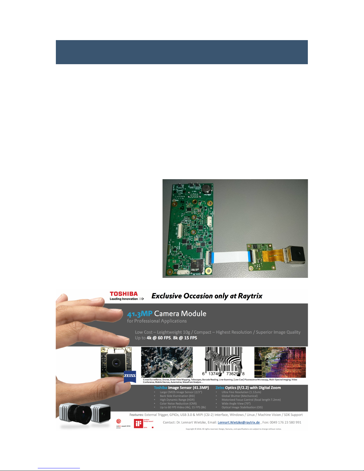
To shiba 4 1 M P i xe l Ca m e ra
Raytrix provides the C41 camera module.
Auvidea has developed a small interface
board to connect the C41 camera module to
the J120. A resolution up the 4kp60 is
supported (2160p60). The Bayer encoded
video is provided raw to the TX1 and
converted in the graphics engine of the
TX1. For more CSI-2 ports please have a
look at the new J140 carrier board with
three 4-lane CSI-2 ports.
!
AUVIDEA GMBH
TECHNICAL REFERENCE MANUAL
9
Page 10
VERSION 1.9
J120 (38198-X)
Devices
IMU (MPU-9250)
A 9 axis sensor is connected to the SPI0 bus of the TX1. Pin 8 (VddIO) of the IMU is connected to 1.8V. Please
set the INT output of the IMU by software to „totem pole“ mode as there is no pull-up on the INT output.
This IMU is optional. Only some J120 models are equipped with this function.
SPI busses with the Jetson TX1
The Jetson TX1 features 3 SPI busses: SPI0 to SPI2. The table below lists how these SPI devices are mounted.
Please note how the 5 physical SPI devices relate to the 5 spidevs.
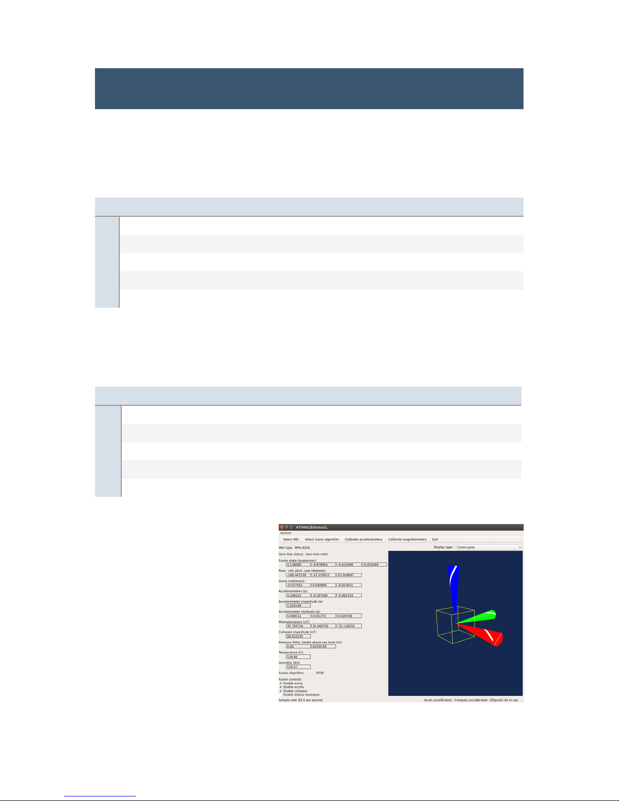
Test of t he IMU wit h t he
RTIMULibDemo
This demo may be downloaded from Github.
Please install qtcreator first. Next please
make sure that the spidev3.0 device in /dev
is loaded. Edit the RTIMUlibDemo.ini file
with the SPI settings for the IMU (bus 3,
select 0). Start the demo as root so it gets
access to the SPI bus.
The IMU chip is located on the bottom side
next to the JTAG connector. The IMU is
optional on the J120. Please make sure that
your J120 has the IMU installed.
Pin
Function
Jetson TX1
Description
9
AD0/SDO
E4
SPI0_MISO (1.8V)
24
SDA/SDI
F4
SPI0_MOSI (1.8V)
23
SCL/SCLK
E3
SPI0_CLK (1.8V)
22
/CS
F3
SPI0_CS0 (1.8V)
12
INT
G14
INT is inverted and connected to GPIO9_MOTION_INT (1.8V)
BusCSTegra X1
SPI device
Use
SPI00SPI4
spidev3.0
IMU MPU-9250
SPI10SPI1
spidev0.0
CAN controller 1 (MCP2515)
SPI11SPI1
spidev0.1
CAN Controller 2 (MCP2515)
SPI20SPI2
spidev1.0
I2C/SPI connector J13
SPI21SPI2
spidev1.1
I2C/SPI connector J14
AUVIDEA GMBH
TECHNICAL REFERENCE MANUAL
10
Page 11

VERSION 1.9
J120 (38198-X)
I2C busses with the Jetson TX1
The Jetson TX1 features 7 I2C devices: I2C0 to I2C6. The table below lists how these I2C devices are mounted.
A B102 module may be connected to the CSI-2 EF connector. The Toshiba TC358743 HDMI to CSI-2 converter
chip is on the 7 bit I2C address 0x0F, as it can be seen in the terminal output below.
$ sudo i2cdetect -y -r 2
!!!!0 !1 !2 !3 !4 !5 !6 !7 !8 !9 !a !b !c !d !e !f
00: !!!!!!!!!-- -- -- -- -- -- -- -- -- -- -- -- 0f
10: -- -- -- -- -- -- -- -- -- -- -- -- -- -- -- -20: -- -- -- -- -- -- -- -- -- -- -- -- -- -- -- -30: -- -- -- -- -- -- -- -- -- -- -- -- -- -- -- -40: -- -- -- -- -- -- -- -- -- -- -- -- -- -- -- -50: 50 51 52 53 -- -- -- -- -- -- -- -- -- -- -- -60: -- -- -- -- -- -- -- -- -- -- -- -- -- -- -- --
70: -- -- -- -- -- -- -- -- !!!!!!!!!
CAN
The J120 features 1 or 2 CAN interfaces. As the Jetson TX1 does not have native CAN interfaces, the J120
features 2 SPI based CAN controllers (Microchip MCP2515). Please install the Kernel and support package with
the MCP2515 driver, which is provided by Auvidea. Because of a bug in the SPI_CS_0 handling only 1 CAN
controller is populated.
$ sudo modprobe mcp251x
$ sudo ip link set can0 up type can bitrate 1000000
$ ifconfig
can0 Link encap:UNSPEC HWaddr 00-00-00-00-00-00-00-00-00-00-00-00-00-00-00-00
UP RUNNING NOARP MTU:16 Metric:1
RX packets:0 errors:0 dropped:0 overruns:0 frame:0
TX packets:0 errors:0 dropped:0 overruns:0 carrier:0
collisions:0 txqueuelen:10
RX bytes:0 (0.0 B) TX bytes:0 (0.0 B)
eth0 Link encap:Ethernet HWaddr 00:04:4b:57:29:32
UP BROADCAST MULTICAST MTU:1500 Metric:1
RX packets:0 errors:0 dropped:0 overruns:0 frame:0
TX packets:0 errors:0 dropped:0 overruns:0 carrier:0
collisions:0 txqueuelen:1000
RX bytes:0 (0.0 B) TX bytes:0 (0.0 B)
lo Link encap:Local Loopback
inet addr:127.0.0.1 Mask:255.0.0.0
Bus
device
physical bus
Use
I2C0
0
I2C0
I2C1
1
I2C1
LM75ADP temperature sensor
I2C2
2
I2C_PM
CSI-2 EF connector
I2C3
3
?
I2C4
4
?
I2C5
5
?
I2C6
6
I2C_CAM
AUVIDEA GMBH
TECHNICAL REFERENCE MANUAL
11
Page 12
VERSION 1.9
J120 (38198-X)
inet6 addr: ::1/128 Scope:Host
UP LOOPBACK RUNNING MTU:65536 Metric:1
RX packets:549 errors:0 dropped:0 overruns:0 frame:0
TX packets:549 errors:0 dropped:0 overruns:0 carrier:0
collisions:0 txqueuelen:0
RX bytes:46707 (46.7 KB) TX bytes:46707 (46.7 KB)
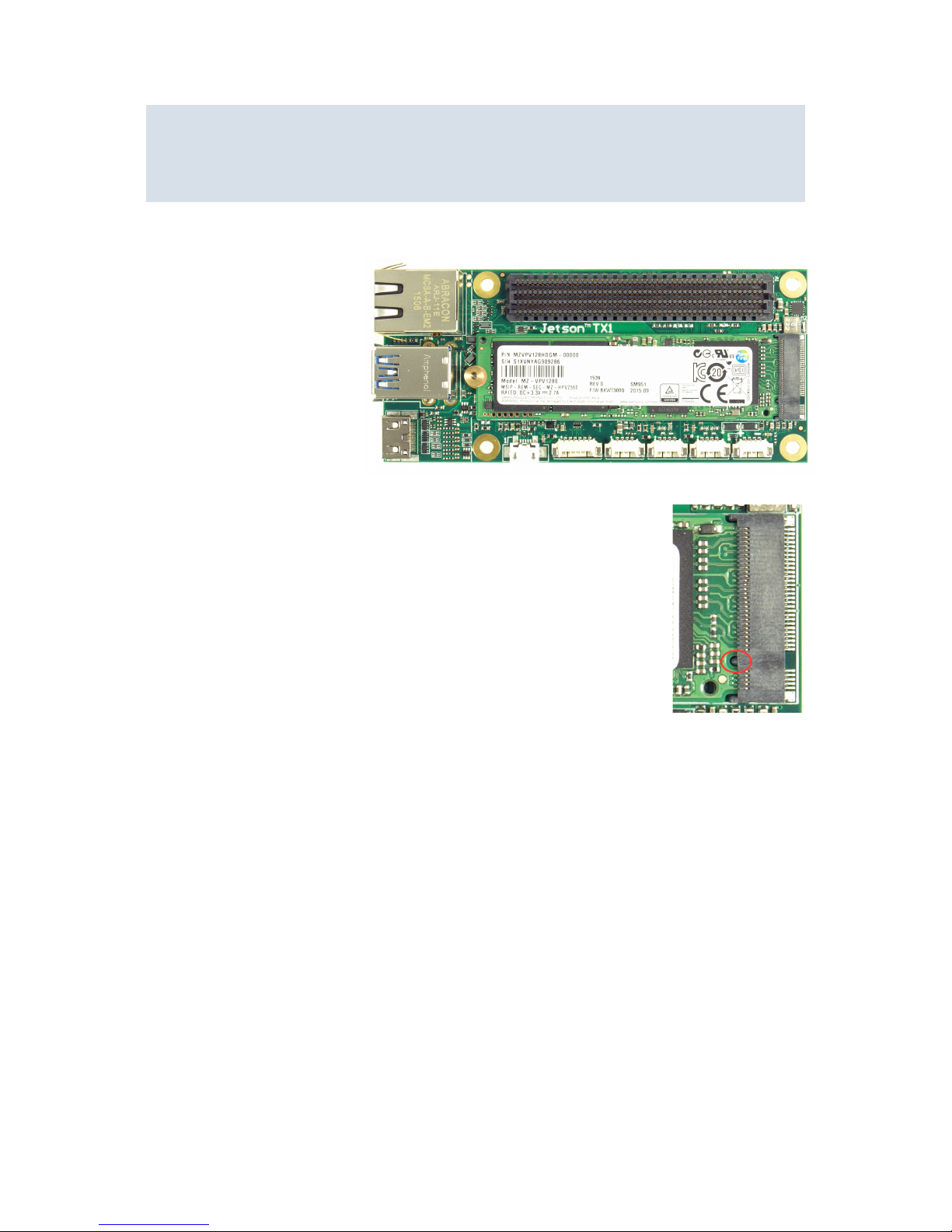
M.2 SSD 2280
The J120 features a very high
performance SSD of the NGFF
(next generation form factor)
kind called now M.2. There are
two types available: SATA and 4x
PCIe. The J120 only supports the
4x PCIe type (type M). We have
tested the Samsung SM951 128GB
module (MZ-VPV1280). Please see
the picture on the right.
How can the type M card be
identified?
M.2 type M card have just one notch on the right side on the bottom. Please see the
picture on the right. M.2 type B (SATA) cards have a notch on the right side on top or
they have two notches. So M.2 type B (SATA) cards may fit mechanically, but they will
not work. Please make sure that the M.2 card for the J120 has just one notch.
Examples of M.2 type M SSDs with PCIe interface:
•
Samsung 950 Pro 256GB (MZ-V5P256BW)
•
Samsung PM961 128GB (MZVLW128HEGR)
•
Samsung SM951 512GB (MZVPV512HDGL)
M.2 NVMe software support on the Jetson TX1
In order to use a M.2 key B SSD on the Jetson TX1, a kernel module supporting NVMe is needed. This module is
not part of the dev kit default kernel configuration, so the kernel module needs to compiled. Because of the
mixture of 32 bit user space and 64 bit kernel, it is recommended to cross compile the kernel on a Ubuntu
14.04 LTS host machine. For details on cross-compiling a kernel for L4T please visit the!Ridgerun wiki.
https://developer.ridgerun.com/wiki/index.php?title=Compiling_Tegra_X1_source_code#Kernel
The required module '.config' parameter is!
CONFIG_BLK_DEV_NVME=y
or in menuconfig under
Device Drivers -> Block Devices -> NVM Express block device!
AUVIDEA GMBH
TECHNICAL REFERENCE MANUAL
12
Page 13
VERSION 1.9
J120 (38198-X)
Connectors
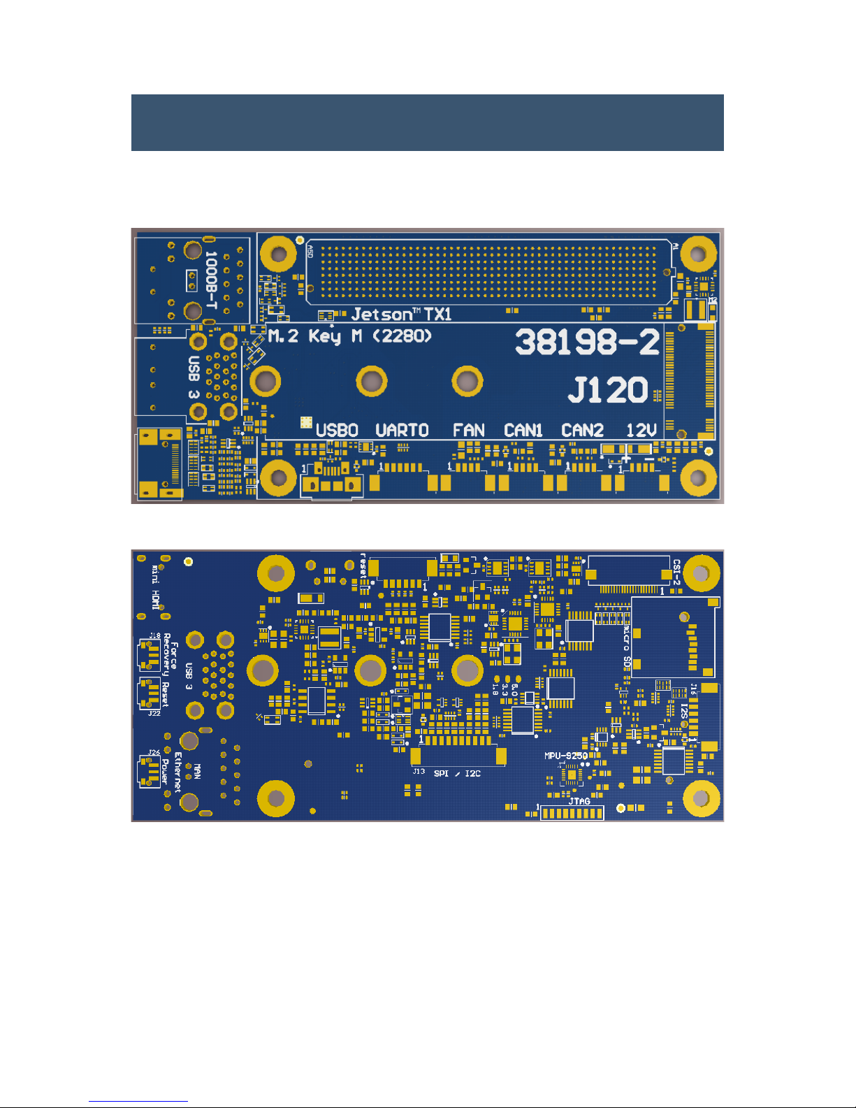
Auvidea supplies cable kits for the connectors with 1.25 mm pitch. Please check the website for details. Figure
1 and 2 show the J120 rev 2 but the connector placement and pin numbering also applies to the J120 rev 1.
Figure 1: connectors on the top side
Figure 2: connectors on the bottom side
AUVIDEA GMBH
TECHNICAL REFERENCE MANUAL
13
Page 14

VERSION 1.9
J120 (38198-X)
USB 3.0 (J2)
This is dual USB 3.0 type a connector. Pin 1-9 is the bottom connector and pin 10-18 is the top connector.
USB 2.0 (J6)
USB 2.0 port for firmware upgrades and for USB 2.0 devices like mouse and keyboard.
Pin
Function
Jetson TX1
Description
15V-
5V power controlled by USB2_EN_OC (A19) - max. 900 mA
2
USB2-D-
B43
USB 2.0 data
3
USB2-D+
B42
USB 2.0 data
4
GND
-
Ground
5
USB3_RX2-
H42
USB 3.0 receive data
6
USB3_RX2+
H41
USB 3.0 receive data
7
GND
-
Ground
8
USB3_TX2-
E42
USB 3.0 transmit data
9
USB3_TX2+
E41
USB 3.0 transmit data
105V-
5V power controlled by USB1_EN_OC (A18) - max. 900 mA
11
USB1-D-
A39
USB 2.0 data
12
USB1-D+
A38
USB 2.0 data
13
GND
-
Ground
14
USB3_RX1-
F44
USB 3.0 receive data
15
USB3_RX1+
F43
USB 3.0 receive data
16
GND
-
Ground
17
USB3_TX1-
C44
USB 3.0 transmit data
18
USB3_TX1+
C43
USB 3.0 transmit data
Pin
Function
Jetson TX1
Description
15V-
5V power controlled by USB0_EN_OC* (A17) - max. 500 mA
2
USB0-D-
B40
USB 2.0 data
3
USB0-D+
B39
USB 2.0 data
4
USB0_ID
A36
connected to 3.3V with 10k pullup
5
GND
-
Ground
-
USB0_VBUS
B37
connected to pin 1 of this connector
AUVIDEA GMBH
TECHNICAL REFERENCE MANUAL
14
Page 15

VERSION 1.9
J120 (38198-X)
CAN controller (MCP2515T-I/ML)
The two SPI to CAN controllers add two CAN bus interfaces to the TX1, as there is no internal CAN controller in
the TX1. The SPI bus, RESET and INT are shared between the 2 CAN controllers (J120 rev 1). The J120 rev 2
will use separate SPI interrupts. Just SPI1_CS0 and SPI1_CS1 select one of the two controllers. The two CAN
busses are available on J9 (CAN1) and J10 (CAN2).
Interrupt: the interrupt outputs of the 2 CAN controllers are tied together and have a common 10k pull-up
resistor (rev 1).
J120 rev 1: on the silkscreen „CAN1“ and „CAN2“ are swapped. CAN1 is next to the FAN connector.
CAN controller 1:
CAN controller 2:
CAN1 (J9):
CAN2 (J10):
Pin
Function
Jetson TX1
Description
15SOF14
SPI1_MISO (level shifted to 3.3V)
14SIF13
SPI1_MOSI (level shifted to 3.3V)
12
SCK
G13
SPI1_CLK (level shifted to 3.3V)
22
/CS
E14
SPI1_CS0 (level shifted to 3.3V)
12
/INT
H3
GPIO20_AUD_INT (low active with 10k pull-up to 3.3V)
17
/RESET
D7
GPIO5_CAM_FLASH_EN is inverted and connected to the RESET inputs
Pin
Function
Jetson TX1
Description
15SOF14
SPI1_MISO (level shifted to 3.3V)
14SIF13
SPI1_MOSI (level shifted to 3.3V)
12
SCK
G13
SPI1_CLK (level shifted to 3.3V)
22
/CS
E13
SPI1_CS1 (level shifted to 3.3V)
12
/INT
H3
GPIO20_AUD_INT (low active with 10k pull-up to 3.3V)
17
/RESET
D7
GPIO5_CAM_FLASH_EN is inverted and connected to the RESET inputs
Pin
Function
Jetson TX1
Description
15V-
5V power for the CAN bus (500 mA)
2
CAN2_H
-
CAN data high
3
CAN2_L
-
CAN data low
4
GND
-
Ground (0V)
Pin
Function
Jetson TX1
Description
15V-
5V power for the CAN bus (500 mA)
2
CAN1_H
-
CAN data high
Pin
AUVIDEA GMBH
TECHNICAL REFERENCE MANUAL
15
Page 16

VERSION 1.9
J120 (38198-X)
3
CAN1_L
-
CAN data low
4
GND
-
Ground (0V)
Function
Jetson TX1
Description
Pin
AUVIDEA GMBH
TECHNICAL REFERENCE MANUAL
16
Page 17

VERSION 1.9
J120 (38198-X)
CSI-EF (J14)
This is a 22 pin 4 lane CSI-2 connector with 0.5mm pitch (Wuerth 687122149022). To open the connector and to
release the cable just lift the brown lid upwards. This connector has the same pinout as the CSI-2 connector on
the Raspberry Pi compute module carrier board. The contacts are on the bottom.
Ethernet (J1)
The J120 features an on-board RJ45 connector for 10/100/1000BT Ethernet with 2 LEDs.
Pin
Function
Jetson TX1
Description
1
3.3V
-
3.3V power supply
2
I2C_PM_DAT
B6
3.3V level (converted from 1.8V of the Jetson TX1) - I2C device 2
3
I2C_PM_CLK
A6
3.3V level (converted from 1.8V of the Jetson TX1) - I2C device 2
4
GND
-
Ground
5
CAM2_MCLK
E7
CAM2_MCLK
6
CAM3_GPIO
H7
GPIO3_CAM1_RST*
7
GND
-
Ground
8
CSI-F_D1+
E21
CSI-2 bus F lane 1
9
CSI-F_D1-
E20
CSI-2 bus F lane 1
10
GND
-
Ground
11
CSI-F-D0-
C23
CSI-2 bus F lane 0
12
CSI-F-D0-
C22
CSI-2 bus F lane 0
13
GND
-
Ground
14
CSI-E_CLK+
G22
CSI-2 bus E clock
15
CSI-E_CLK-
G21
CSI-2 bus E clock
16
GND
-
Ground
17
CSI-E-D1+
H21
CSI-2 bus E lane 1
18
CSI-E-D1-
H20
CSI-2 bus E lane 1
19
GND
-
Ground
20
CSI-E-D0+
F23
CSI-2 bus E lane 0
21
CSI-E-D0-
F22
CSI-2 bus E lane 0
22
GND
-
Ground
LED
Function
Jetson TX1
Description
GBE0
GBE_LINK_ACT*
E47
left LED
GBE1
GBE_LINK_100
F50
right LED
AUVIDEA GMBH
TECHNICAL REFERENCE MANUAL
17
Page 18

VERSION 1.9
J120 (38198-X)
HDMI (J3)
This is a 19 pin mini HDMI connector. Please note that the HDMI and mini HDMI connector have different pin
outs.
UART 0 (J7)
This is a 6 pin connector with 1.25 mm pitch. Please connect to USB TTL serial converter (3.3V TTL level).
Normally just connect TXD, RXD, and GND. Swap data lines. Default speed: 115200 bps. This is the
configuration for the J120 rev 1 and J120 rev 2 with a serial number < 2021.
Pin
Function
Jetson TX1
Description
1
GND
-
Ground
2
DP1_TXD0+
E39
HDMI data lane 2
3
DP1_TXD0-
E38
HDMI data lane 2
4
GND
-
Ground
5
DP1_TXD1+
C38
HDMI data lane 1
6
DP1_TXD1-
C37
HDMI data lane 1
7
GND
-
Ground
8
DP1_TXD2+
D37
HDMI data lane 0
9
DP1_TXD2-
D36
HDMI data lane 0
10
GND
-
Ground
11
DP1_TXD3+
E36
HDMI clock
12
DP1_TXD3-
E35
HDMI clock
13
GND
-
Ground
14
CEC
B33
HDMI_CEC
15
HDMI_DDC_SCL
A35
DP1_AUX_CH
16
HDMI_DDC_SDA
A34
DP1_AUX_CH*
17
reserved
-
not connected
18
PWR
-
5V power (max. 500 mA)
19
HPD
A33
inverted and connected to DP1_HPD
Pin
Function
Jetson TX1
GPIO
Description
15V-
-
5V power output
2
UART0_TXD
H12
GPIO3_PU.00
UART 0 console port (3.3V TTL level): transmit data output
3
UART0_RXD
G12
GPIO3_PU.01
UART 0 console port (3.3V TTL level): receive data input
4
UART0_CTS
H11
GPIO3_PU.03
UART 0 console port (3.3V TTL level): clear to send
5
UART0_RTS
G11
GPIO3_PU.02
UART 0 console port (3.3V TTL level): ready to send
6
GND--
Ground
AUVIDEA GMBH
TECHNICAL REFERENCE MANUAL
18
Page 19

VERSION 1.9
J120 (38198-X)
UART 0 / UART 2 (J7) - rev 2 to 5
This is the configuration for the J120 rev 2 with a serial number > 2020. All 4 pins are passed through a bidirectional level converter with 3.3V level outputs (TXB0104PWR) and through 33 Ohm series resistors (in a
tiny 0804 size resistor array). To limit the power dissipation in the resistor array, it is advised to sink or source
a maximum current of 1 mA.
UART 0 (J7) - rev 6
This is the configuration for the J120 rev 6. 2 pins are passed through a bi-directional level converter with
3.3V level outputs (TXB0104PWR) and through 33 Ohm series resistors (in a tiny 0804 size resistor array). To
limit the power dissipation in the resistor array, it is advised to sink or source a maximum current of 1 mA. Pin
4 and 5 provide the programming interface for the watchdog MCU (STM42F042).
UART 0 / UART 2 (J7) - rev 7
This is the configuration for the J120 rev 7. All 4 pins are passed through a bi-directional level converter with
3.3V level outputs (TXB0104PWR) and through 33 Ohm series resistors (in a tiny 0804 size resistor array). To
limit the power dissipation in the resistor array, it is advised to sink or source a maximum current of 1 mA. Pin
4 and 5 have the dual function to flash the watchdog MCU.
If the tunnelling of the UART0 port causes difficulties in a particular use case, the J120 can be reconfigured so
that the MCU is bypassed and a direct connection to the UART0 port of the TX1 and TX2 is provided. Please
check appendix A for details on the watchdog MCU.
Pin
Function
Jetson TX1
GPIO
Description
15V-
-
5V power output
2
UART0_TXD
H12
GPIO3_PU.00
UART 0 console port (3.3V TTL level): transmit data output
3
UART0_RXD
G12
GPIO3_PU.01
UART 0 console port (3.3V TTL level): receive data input
4
UART2_TXD
B16
-
UART 2 console port (3.3V TTL level): transmit data output
5
UART2_RXD
B15
-
UART 2 console port (3.3V TTL level): receive data output
6
GND--
Ground
Pin
Function
Jetson TX1
GPIO
Description
15V-
-
5V power output (3.3V if only the MCU is powered)
2
UART0_TXD--
UART 0 console port (3.3V TTL level): transmit data output
- tunnelled though the watchdog MCU
3
UART0_RXD--
UART 0 console port (3.3V TTL level): receive data input tunnelled through the watchdog
4
SWCLK--
port to flash watchdog MCU
5
SWDIO--
port to flash watchdog MCU
6
GND--
Ground
AUVIDEA GMBH
TECHNICAL REFERENCE MANUAL
19
Page 20

VERSION 1.9
J120 (38198-X)
FAN (J8)
This is a 4 pin connector with 1.25 mm pitch. This is the same pinout as the fan connector on the Jetson TX1
development kit. With the J100 the fan is on by default. Use the „fan disable“ feature to turn off the fan.
Please note, that the „fan disable“ requires a software change when compared to the dev kit. On the dev kit
„fan disable“ is controlled by an I2C port expander line. On the J100 „fan disable“ is connected to
GPIO19_AUD_RST (through an inverting MOSFET). Pull the GPIO19 (F2) high to disable the fan (pin 4 becomes
low). A low or floating signal on GPIO19 will not disable the fan.
Power (J11)
This is a 4 pin connector with 1.25 mm pitch. Power in 1 and power in 2 are or’ed with 2 Schottky diodes. They
may be tied together or they may be connected to 2 redundant power supplies.
Pin
Function
Jetson TX1
GPIO
Description
15V-
-
5V power output (3.3V if only the MCU is powered)
2
UART0_TXD--
UART 0 console port (3.3V TTL level): transmit data output
- tunnelled through the watchdog
3
UART0_RXD--
UART 0 console port (3.3V TTL level): receive data input tunnelled through the watchdog
4
UART2_TXD
SWCLK
B16
-
UART 2 console port (3.3V TTL level): transmit data output
- port to flash watchdog MCU
5
UART2_RXD
SWDIO
B15
-
UART 2 console port (3.3V TTL level): receive data output port to flash watchdog MCU
6
GND--
Ground
Pin
Function
Jetson TX1
Description
1
GND
-
Ground
25V-
5V power supply to the fan
3
FAN_ TACH
B17
tachometer from the fan (open drain input with 100k pull-up to 1.8V)
4
FAN_ PWM
C16
PWM control to the fan (open drain output: controlled by FAN_PWM
and „disable fan“ with GPIO19 - F2)
Pin
Function
Jetson TX1
Description
1
power in 1
-
power input: typical 12V (range: 7V to 17V)
2
power in 2
-
power input: typical 12V (range: 7V to 17V)
3
GND
-
power ground
4
GND
-
power ground
AUVIDEA GMBH
TECHNICAL REFERENCE MANUAL
20
Page 21

VERSION 1.9
J120 (38198-X)
I2S (J16)
This is a 6 pin connector with 1.25 mm pitch. All signals are covered from 1.8V (TX1) to 3.3V (connector) with
a bi-directional level converter. The data direction is automatically determined by the level converter.
J120 rev 1, 2, 3 and 4:
J120 rev 5 (38198-5) and newer:
SPI/I2C (J13)
This is a 10 pin connector with 1.25 mm pitch.
Note: J120 rev 1, 2, and 3: pin 8 and pin 9 have 1k pullup (rev 4 and newer: 10k)
Pin
Function
Jetson TX1
GPIO
Description
1
3.3V--
3.3V power supply
2
I2S_MCLK
F1
GPIO3_PBB.00
digital audio interface: master clock (3.3V)
3
I2S2_SING6-
digital audio interface 0: audio input (3.3V)
4
I2S2_CLKG5-
digital audio interface 0: bit clock (3.3V)
5
I2S2_LRCLKH5-
digital audio interface 0: word clock (3.3V)
6
GND--
Ground
Pin
Function
Jetson TX1
GPIO
Description
1
3.3V--
3.3V power supply
2
I2S_MCLK
F1
GPIO3_PBB.00
digital audio interface: master clock (3.3V)
3
I2S0_SIN
G1
GPIO3_PB.01
digital audio interface 0: audio input (3.3V)
4
I2S0_CLK
G2
GPIO3_PB.03
digital audio interface 0: bit clock (3.3V)
5
I2S0_LRCLK
H1
GPIO3_PB.00
digital audio interface 0: word clock (3.3V)
6
GND--
Ground
Pin
Function
Jetson TX1
GPIO
Description
1
5.0V--
5.0V power supply
2
SPI2_CLK
H14
-
SPI2_CLK (level shifted to 3.3V)
3
SPI2_MISO
H15
-
SPI2_CLK (level shifted to 3.3V)
4
SPI2_MOSI
G15
-
SPI2_CLK (level shifted to 3.3V)
5
SPI2_CS0
G16
-
SPI2_CLK (level shifted to 3.3V)
6
SPI2_CS1
F16
-
SPI2_CLK (level shifted to 3.3V)
7
INT_SPI2
H13
GPIO3_PX.03
GPIO8_ALS_PROX_INT (due to level converter input only)
8
I2C0_CLK
E15
-
I2C0_CLK (level shifted to 3.3V with 10k pullup)
9
I2C0_DAT
F15
-
I2C0_DAT (level shifted to 3.3V with 10k pullup)
10
GND--
Ground
AUVIDEA GMBH
TECHNICAL REFERENCE MANUAL
21
Page 22

VERSION 1.9
J120 (38198-X)
Micro SD card (J15)
Micro SD card reader (Amphenol 101-00660-68-6). SDCARD_WP (F20) = 0 (inactive).
Buttons (J12)
6 pin connector with 1.25 mm pitch (on the bottom side next to the green LED).
M.2 type M 2280 (J15)
J120 rev 1: this slot is non functional due to power limitations of the integrated 3.3V power supply.
J120 rev 2: this will be fixed by adding a 3.3V 3A power supply.
Form factor: 2242, 2260 or 2280 (22 x 80 mm)
Interface: four PCIe lanes for top performance (no SATA support)
Pin
Function
Jetson TX1
Description
1
SD_DAT2
F19
SD card interface data 2
2
SD_DAT3
F18
SD card interface data 3
3
SD_CMD
G19
SD card interface command
4
3.3V
-
enabled by SDCARD_PWR_EN = 1 (H16)
5
SD_CLK
G18
SD card interface clock
6
GND
-
Ground
7
SD_DAT0
H18
SD card interface data 0
8
SD_DAT1
H17
SD card interface data 1
9
SD_CD
F17
GND
Pin
Function
Jetson TX1
GPIO
Description
1
Vdd_RTC
A50
-
Realtime clock power input from backup battery or
super cap
Do not connect if super cap or Lithium cell (J60) is
populated on the J120. (rev 1: connected to GND)
2
power
B50
GPIO3_PX.05
power button (connect to GND)
3
sleep
E2
GPIO3_PY.00
sleep button (connect to GND)
4
force recv.
E1
GPIO3_PX.06
force recovery button (connect to GND)
5
reset
A47
-
reset in button (connect to GND)
6
GND--
Ground
AUVIDEA GMBH
TECHNICAL REFERENCE MANUAL
22
Page 23

VERSION 1.9
J120 (38198-X)
JTAG header (P1)
This is a 9 pin connector with 1.25 mm pitch with surface mount pads on the edge of the board.
Pin
Function
Jetson TX1
Description11.8V
-
1.8V power output
2
JTAG_AP_TRST_L
B13
JTAG port of Jetson TX1
3
JTAG_AP_TCK
B11
JTAG port of Jetson TX2
4
JTAG_AP_RTCK
A14
JTAG port of Jetson TX3
5
JTAG_AP_TDO
A13
JTAG port of Jetson TX4
6
JTAG_AP_TMS
A12
JTAG port of Jetson TX5
7
NVJTAG_SEL
A11
JTAG port of Jetson TX6
8
JTAG_AP_TDI
B12
JTAG port of Jetson TX7
9
GND
-
Ground
AUVIDEA GMBH
TECHNICAL REFERENCE MANUAL
23
Page 24

VERSION 1.9
J120 (38198-X)
MCU
The J90 features an on-board micro controller (MCU: STM32F042F6P6) with 32 kByte Flash and 6kByte RAM.
MCU pin description
Pin types:
PP - push/pull output#
OD - open drain output#
Ain - analog input#
AF - alternate function
The power supply to the MCU is supplied by a 3.3V LDO regulator which is always on. So the MCU is powered as
soon as power is applied to the power input on J13. This allows the MCU to manage whether power should be
applied to the carrier board (with pin 7).
The MCU tunnels the console UART interface to the TX1/TX2. Some instructions are intercepted by the MCU
and executed by it. These instructions are not forwarded to the TX1/TX2.
MCU Pin
Name
Typ e
Function
Description
1
PB8/BOOT0
--10k pull down
2
PF0
OD
POWER
1: inactive, 0: press power button
3
PF1
PP
RESET
1: press reset button (10k pull down), 0: inactive
4
NRST--
hardware power on reset of MCU (RC circuit)
5
VddA--
analog 3.3V supply (by always on LDO)
6
PA 0
Ain0
V12_IN
measure input voltage (voltage divider: 100k up/10k down)
7
PA 1
PP
PWR_ON
1: enable power to J90 (10k pull down), 0: power off
8
PA 2
AF
UART0_RX
UART 0 to TX1/TX2
9
PA 3
AF
UART0_TX
UART 0 to TX1/TX2
10
PA 4PPLED
0: LED off, 1: LED on (default MCU heartbeat)
11
PA 5
AIN5
V3.3_IN
measure 3.3V rail (voltage divider: 10k up/10k down)
12
PA 6
AIN6
V5_IN
measure 5.0V rail (voltage divider: 10k up/10k down)
13
PA 7ODSLEEP
0: press sleep button (R30 must be installed), 1: inactive
14
PB1
Ain9
V1.8_IN
measure 1.8V rail (direct connection)
15
GND--
Ground
16
VddA--
digital 3.3V supply (by always on LDO)
17
PA 9/ PA1 1
AF
UART_TX
UART_TX to J7 connector (pin 2)
18
PA 10 /PA 12
AF
UART_RX
UART_RX to J7 connector (pin 3)
19
PA 13
-
SWDIO
SWD programming interface (J7 pin 5)
20
PA 14
-
SWCLK
SWD programming interface (J7 pin 4)
AUVIDEA GMBH
TECHNICAL REFERENCE MANUAL
24
Page 25

VERSION 1.9
J120 (38198-X)
MCU command set
mcu --adc read the 4 voltage rails (power in, 5V, 3.3V, and 1.8V)
mcu --reset reset TX1/TX2
mcu --poweron power on TX1/TX2
mcu --shutdown power off TX1/TX2
mcu --version display firmware version
mcu --help display list of command available
MCU firmware upgrade
The C source code for the MCU is available on request (Attolic TrueStudio project). Please contact us. The MCU
may be programmed with the ST/LINK programming adapter (SWCLK, SWDIO, GND). We recommend the use of
the STM32VLDISCOVERY discovery kit for STM32F100 Value line. It is available in the Auvidea online shop and at
digikey.com (497-10633-ND). To connect to the J120, please remove the 2 CN3 jumpers and connect SWCLK,
SWDIO and GND to the 4 pin CN2 header.
MCU firmware v1.1
This version of the MCU is limited to a UART baud rate of 38400 baud max. Please set the TX1/TX2 to 38400.
Please edit the file /boot/extlinux/extlinux.conf. Please replace 115200n8 by 38400n8.
TIMEOUT 30
DEFAULT primary
MENU TITLE p2371-2180 eMMC boot options
LABEL primary
MENU LABEL primary kernel
LINUX /boot/Image
INITRD /boot/initrd
FDT /boot/tegra210-jetson-auvidea-j90.dtb
APPEND fbcon=map:0 console=tty0 console=ttyS0,115200n8
MCU firmware v1.3
This version of the MCU uses the standard baud rate of 115200 baud. The firmware is installed on the J120 rev
7 and newer.
If your use case requires a direct connection to the UART0 of the TX1 and TX2 then there are the following
options:
1.
please order a J120 without the MCU populated
2.
if you have received a J120 with the MCU populated, the MCU may be bypassed. Please follow the
instructions in Appendix A.
AUVIDEA GMBH
TECHNICAL REFERENCE MANUAL
25
Page 26
VERSION 1.9
J120 (38198-X)
Appendix A
Bypass of UART0 (watchdog MCU)
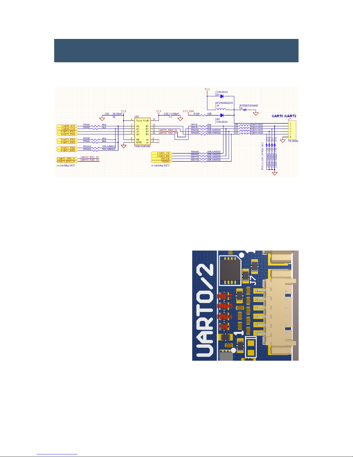
The schematics above show the circuit details of the UART0/2 connector (J7). In the standard UART0
configuration the UART0 port of the TX1/TX2 is connected to the MCU. The MCU is programmed to tunnel all
output on UART0 to it second UART port, which then connects to the J7 connector. The MCU was introduced as
an option with rev 6 and became a standard feature with rev 7.
If you experience problems with the UART0 port and your use case requires a direct connection to UART0 the
MCU may be bypassed by the following steps:
1.
please flash the MCU (STM32F042) with the J90-J140-MCU-UART-OFF firmware. This disables the UART ports
of the MCU so that it may be bypassed. Alternatively the MCU may be removed.
2.
please populate RN1 with a 10 Ohm resistor network
(Panasonic: EXB-24V100JX, Digikey: Y5100CT-ND,
Auvidea: 25151), to connect the UART0 port of the TX1/
TX2 to J7. Please note that this requires very good
soldering skills and it should be performed by our
technicians. Please contact our support team.
AUVIDEA GMBH
TECHNICAL REFERENCE MANUAL
26
Page 27

VERSION 1.9
J120 (38198-X)
FAQ
1.
to be added
!
AUVIDEA GMBH
TECHNICAL REFERENCE MANUAL
27
Page 28

VERSION 1.9
J120 (38198-X)
Disclaimer
Thank you for reading this manual. If you have found any typos or errors in this document, please let us know.
This is the preliminary version of this data sheet. Please treat all specifications with caution as there may be
any typos or errors.
The Auvidea Team
AUVIDEA GMBH
TECHNICAL REFERENCE MANUAL
28
 Loading...