

Page 1

DL305
Analog I/O Modules
Manual Number D3--ANLG-M
Page 2

WARNING
Thank you for purchasing automation equipment from Automationdirect.comä. We want your new DirectLOGICä
automation equipment to operate safely. Anyone who installs or uses this equipment should read this publication (and
any other relevant publications) before installing or operating the equipment.
To minimize the risk of potential safety problems, you should follow all applicable local and national codes that regulate
the installation and operation of your equipment. These codes vary from area to area and usually change with time. It is
your responsibility to determine which codes should be followed, and to verify that the equipment, installation, and
operation is in compliance with the latest revision of these codes.
At a minimum, you should follow all applicable sections of the National Fire Code, National Electrical Code, and the
codes of the National Electrical Manufacturer’s Association (NEMA). There may be local regulatory or government
offices that can also help determine which codes and standards are necessary for safe installation and operation.
Equipment damage or serious injury to personnel can result from the failure to follow all applicable codes and
standards. We do not guarantee the products described in this publication are suitable for your particular application,
nor do we assume any responsibility for your product design, installation, or operation.
If you have any questions concerning the installation or operation of this equipment, or if you need additional
information, please call us at 1--770--844--4200 or FAX 1--770--886--3199.
This publication is based on information that was available at the time it was printed. At Automationdirect.comä we
constantly strive to improve our products and services, so we reserve the right to make changes to the products and/or
publications at any time without notice and without any obligation. This publication may also discuss features that may
not be available in certain revisions of the product.
Trademarks
This publication may contain references to products produced and/or offered by other companies. The product and
company names may be trademarked and are the sole property of their respective owners. Automationdirect.comä
disclaims any proprietary interest in the marks and names of others.
Stage is a trademark of Koyo Electronics Industries Co., LTD. Think & Do Software is a trademark of Think & Do
Software, Inc. Texas Instruments is a registered trademark of Texas Instruments, Inc. TI, TIWAY, Series 305, Series
405, TI305, and TI405 are trademarks of Texas Instruments, Inc. Siemens and SIMATIC are registered trademarks of
Siemens, AG. GE is a registered trademark of General Electric Corporation. Series One is a registered trademark of
GE Fanuc Automation North America, Inc. MODBUS is a registered trademark of Gould, Inc. IBM is a registered
trademark of International Business Machines. MS-DOS and Microsoft are registered trademarks of Microsoft
Corporation. Windows and Windows NT are trademarks of Microsoft Corporation. OPTOMUX and PAMUX are
trademarks of OPTO 22.
Copyright 1999, Automationdirect.comä Incorporated
No part of this manual shall be copied, reproduced, or transmitted in any way without the prior, written consent of
Automationdirect.comä Incorporated. Automationdirect.comä retains the exclusive rights to all information
included in this document.
All Rights Reserved
Page 3
1
M
a
n
u
a
l
R
e
v
i
s
i
o
n
s
If you contact us in reference to this manual, be sure to include the revision number.
Title: DL305 Analog I/O Modules, 2nd Edition, Rev. C
Manual Number: D3--ANLG--M
Issue Date Effective Pages Description of Changes
Original 1/94 Cover/Copyright
Contents
Manual Revisions
1-1 -- 1-9
2-1 -- 2-18
3-1 -- 3-20
4-1 -- 4-15
5-1 -- 5-21
6-1 -- 6-12
7-1 -- 7-14
8-1 -- 8-17
9-1 -- 9-16
10-1 -- 10-14
A-1 -- A-10
2nd Edition 3/96 Cover/Copyright
Contents
Manual Revisions
1-1 -- 1-9
2-1 -- 2-18
3-1 -- 3-20
4-1 -- 4-15
5-1 -- 5-21
6-1 -- 6-13
7-1 -- 7-14
8-1 -- 8-18
9-1 -- 9-16
10-1 -- 10-14
A-1 -- A-10
Original Issue
2nd Edition
Rev. A 4/96 Manual Revisions
Rev. B 6/98 Entire Manual
Rev. C 11/99 3--13,18; 4--11,12,17;
7--13
8--17
Manual Revisions
7--10, 7--11, 7--13 and 8--17
5-16to19,24; 9-12,13;
10--14to16; Appx. A--11to19
Rev. A
Changed last instruction to DOUT3
Changed last instruction to DOUT3
Downsized to spiral
Rev. B
Corrected sequencing examples
Added example programs for the D3--350
CPU.
Page 4

1
T
a
b
l
e
o
f
C
o
n
t
e
n
t
s
Chapter 1: Getting Started
Introduction 1--2. . . . . . . . . . . . . . . . . . . . . . . . . . . . . . . . . . . . . . . . . . . . . . . . . . . . . . . . . . . . . . . . . . . . . . . . .
Purpose of this manual 1--3. . . . . . . . . . . . . . . . . . . . . . . . . . . . . . . . . . . . . . . . . . . . . . . . . . . . . . . . . . . . .
Who should read this manual 1--3. . . . . . . . . . . . . . . . . . . . . . . . . . . . . . . . . . . . . . . . . . . . . . . . . . . . . . .
How this manual is organized 1--3. . . . . . . . . . . . . . . . . . . . . . . . . . . . . . . . . . . . . . . . . . . . . . . . . . . . . . .
Supplemental Manuals 1--3. . . . . . . . . . . . . . . . . . . . . . . . . . . . . . . . . . . . . . . . . . . . . . . . . . . . . . . . . . . . .
DL305 Analog Components 1--4. . . . . . . . . . . . . . . . . . . . . . . . . . . . . . . . . . . . . . . . . . . . . . . . . . . . . . . . . .
DL305 Analog I/O 1--4. . . . . . . . . . . . . . . . . . . . . . . . . . . . . . . . . . . . . . . . . . . . . . . . . . . . . . . . . . . . . . . . .
Thermocouple Input 1--4. . . . . . . . . . . . . . . . . . . . . . . . . . . . . . . . . . . . . . . . . . . . . . . . . . . . . . . . . . . . . . .
Temperature Input 1--4. . . . . . . . . . . . . . . . . . . . . . . . . . . . . . . . . . . . . . . . . . . . . . . . . . . . . . . . . . . . . . . . .
Physical Characteristics 1--5. . . . . . . . . . . . . . . . . . . . . . . . . . . . . . . . . . . . . . . . . . . . . . . . . . . . . . . . . . . . .
Selecting the Appropriate Module 1--6. . . . . . . . . . . . . . . . . . . . . . . . . . . . . . . . . . . . . . . . . . . . . . . . . . . .
Analog Input 1--6. . . . . . . . . . . . . . . . . . . . . . . . . . . . . . . . . . . . . . . . . . . . . . . . . . . . . . . . . . . . . . . . . . . . . .
Analog Output 1--7. . . . . . . . . . . . . . . . . . . . . . . . . . . . . . . . . . . . . . . . . . . . . . . . . . . . . . . . . . . . . . . . . . . .
Special Input 1--7. . . . . . . . . . . . . . . . . . . . . . . . . . . . . . . . . . . . . . . . . . . . . . . . . . . . . . . . . . . . . . . . . . . . .
Analog Made Easy -- Four Simple Steps 1--8. . . . . . . . . . . . . . . . . . . . . . . . . . . . . . . . . . . . . . . . . . . . . . .
Analog Input Terminology 1--9. . . . . . . . . . . . . . . . . . . . . . . . . . . . . . . . . . . . . . . . . . . . . . . . . . . . . . . . . . . .
Channels per Module 1--9. . . . . . . . . . . . . . . . . . . . . . . . . . . . . . . . . . . . . . . . . . . . . . . . . . . . . . . . . . . . . .
Input Ranges 1--9. . . . . . . . . . . . . . . . . . . . . . . . . . . . . . . . . . . . . . . . . . . . . . . . . . . . . . . . . . . . . . . . . . . . .
Resolution 1--9. . . . . . . . . . . . . . . . . . . . . . . . . . . . . . . . . . . . . . . . . . . . . . . . . . . . . . . . . . . . . . . . . . . . . . . .
Input Type 1--9. . . . . . . . . . . . . . . . . . . . . . . . . . . . . . . . . . . . . . . . . . . . . . . . . . . . . . . . . . . . . . . . . . . . . . . .
Input Impedance 1--9. . . . . . . . . . . . . . . . . . . . . . . . . . . . . . . . . . . . . . . . . . . . . . . . . . . . . . . . . . . . . . . . . .
Conversion Method 1--9. . . . . . . . . . . . . . . . . . . . . . . . . . . . . . . . . . . . . . . . . . . . . . . . . . . . . . . . . . . . . . . .
Conversion Time 1--9. . . . . . . . . . . . . . . . . . . . . . . . . . . . . . . . . . . . . . . . . . . . . . . . . . . . . . . . . . . . . . . . . .
Linearity Error and Total Tolerance (Relative Accuracy) 1--9. . . . . . . . . . . . . . . . . . . . . . . . . . . . . . . . .
Accuracy vs. Temperature 1--9. . . . . . . . . . . . . . . . . . . . . . . . . . . . . . . . . . . . . . . . . . . . . . . . . . . . . . . . . .
LED Display 1--9. . . . . . . . . . . . . . . . . . . . . . . . . . . . . . . . . . . . . . . . . . . . . . . . . . . . . . . . . . . . . . . . . . . . . .
I/O Points Required 1--9. . . . . . . . . . . . . . . . . . . . . . . . . . . . . . . . . . . . . . . . . . . . . . . . . . . . . . . . . . . . . . . .
External Power Source 1--9. . . . . . . . . . . . . . . . . . . . . . . . . . . . . . . . . . . . . . . . . . . . . . . . . . . . . . . . . . . . .
Base Power Required 1--9. . . . . . . . . . . . . . . . . . . . . . . . . . . . . . . . . . . . . . . . . . . . . . . . . . . . . . . . . . . . . .
Operating Temperature 1--9. . . . . . . . . . . . . . . . . . . . . . . . . . . . . . . . . . . . . . . . . . . . . . . . . . . . . . . . . . . .
Relative Humidity 1--9. . . . . . . . . . . . . . . . . . . . . . . . . . . . . . . . . . . . . . . . . . . . . . . . . . . . . . . . . . . . . . . . .
Terminal Type 1--9. . . . . . . . . . . . . . . . . . . . . . . . . . . . . . . . . . . . . . . . . . . . . . . . . . . . . . . . . . . . . . . . . . . . .
Weight 1--9. . . . . . . . . . . . . . . . . . . . . . . . . . . . . . . . . . . . . . . . . . . . . . . . . . . . . . . . . . . . . . . . . . . . . . . . . . .
Analog Output Module Terminology 1--10. . . . . . . . . . . . . . . . . . . . . . . . . . . . . . . . . . . . . . . . . . . . . . . . . .
Channels per Module 1--10. . . . . . . . . . . . . . . . . . . . . . . . . . . . . . . . . . . . . . . . . . . . . . . . . . . . . . . . . . . . . .
Output Ranges 1--10. . . . . . . . . . . . . . . . . . . . . . . . . . . . . . . . . . . . . . . . . . . . . . . . . . . . . . . . . . . . . . . . . . . .
Resolution 1--10. . . . . . . . . . . . . . . . . . . . . . . . . . . . . . . . . . . . . . . . . . . . . . . . . . . . . . . . . . . . . . . . . . . . . . . .
Output Current 1--10. . . . . . . . . . . . . . . . . . . . . . . . . . . . . . . . . . . . . . . . . . . . . . . . . . . . . . . . . . . . . . . . . . . .
Output Impedance 1--10. . . . . . . . . . . . . . . . . . . . . . . . . . . . . . . . . . . . . . . . . . . . . . . . . . . . . . . . . . . . . . . .
Load Impedance 1--10. . . . . . . . . . . . . . . . . . . . . . . . . . . . . . . . . . . . . . . . . . . . . . . . . . . . . . . . . . . . . . . . . .
Conversion Time 1--10. . . . . . . . . . . . . . . . . . . . . . . . . . . . . . . . . . . . . . . . . . . . . . . . . . . . . . . . . . . . . . . . . .
Accuracy 1--10. . . . . . . . . . . . . . . . . . . . . . . . . . . . . . . . . . . . . . . . . . . . . . . . . . . . . . . . . . . . . . . . . . . . . . . . .
Accuracy vs. Temperature 1--10. . . . . . . . . . . . . . . . . . . . . . . . . . . . . . . . . . . . . . . . . . . . . . . . . . . . . . . . . .
LED Display 1--10. . . . . . . . . . . . . . . . . . . . . . . . . . . . . . . . . . . . . . . . . . . . . . . . . . . . . . . . . . . . . . . . . . . . . .
Page 5

i
i
Table of Contents
External Power Source 1--10. . . . . . . . . . . . . . . . . . . . . . . . . . . . . . . . . . . . . . . . . . . . . . . . . . . . . . . . . . . . .
Base Power Required 1--10. . . . . . . . . . . . . . . . . . . . . . . . . . . . . . . . . . . . . . . . . . . . . . . . . . . . . . . . . . . . . .
Operating Temperature 1--10. . . . . . . . . . . . . . . . . . . . . . . . . . . . . . . . . . . . . . . . . . . . . . . . . . . . . . . . . . . .
Relative Humidity 1--10. . . . . . . . . . . . . . . . . . . . . . . . . . . . . . . . . . . . . . . . . . . . . . . . . . . . . . . . . . . . . . . . .
Terminal Type 1--10. . . . . . . . . . . . . . . . . . . . . . . . . . . . . . . . . . . . . . . . . . . . . . . . . . . . . . . . . . . . . . . . . . . . .
Weight 1--10. . . . . . . . . . . . . . . . . . . . . . . . . . . . . . . . . . . . . . . . . . . . . . . . . . . . . . . . . . . . . . . . . . . . . . . . . . .
I/O Points Required 1--10. . . . . . . . . . . . . . . . . . . . . . . . . . . . . . . . . . . . . . . . . . . . . . . . . . . . . . . . . . . . . . . .
Chapter 2: D3--04AD 4-Channel Analog Input
Module Specifications 2--2. . . . . . . . . . . . . . . . . . . . . . . . . . . . . . . . . . . . . . . . . . . . . . . . . . . . . . . . . . . . . . .
Analog Input Configuration Requirements 2--2. . . . . . . . . . . . . . . . . . . . . . . . . . . . . . . . . . . . . . . . . . . .
Setting the Module Jumpers 2--3. . . . . . . . . . . . . . . . . . . . . . . . . . . . . . . . . . . . . . . . . . . . . . . . . . . . . . . . .
Connecting the Field Wiring 2--3. . . . . . . . . . . . . . . . . . . . . . . . . . . . . . . . . . . . . . . . . . . . . . . . . . . . . . . . . .
Wiring Guidelines 2--3. . . . . . . . . . . . . . . . . . . . . . . . . . . . . . . . . . . . . . . . . . . . . . . . . . . . . . . . . . . . . . . . .
User Power Supply Requirements 2--3. . . . . . . . . . . . . . . . . . . . . . . . . . . . . . . . . . . . . . . . . . . . . . . . . . .
Custom Input Ranges 2--4. . . . . . . . . . . . . . . . . . . . . . . . . . . . . . . . . . . . . . . . . . . . . . . . . . . . . . . . . . . . . .
Current Loop Transmitter Impedance 2--5. . . . . . . . . . . . . . . . . . . . . . . . . . . . . . . . . . . . . . . . . . . . . . . .
Removable Connector 2--6. . . . . . . . . . . . . . . . . . . . . . . . . . . . . . . . . . . . . . . . . . . . . . . . . . . . . . . . . . . . .
Wiring Diagram 2--6. . . . . . . . . . . . . . . . . . . . . . . . . . . . . . . . . . . . . . . . . . . . . . . . . . . . . . . . . . . . . . . . . . .
Module Operation 2--7. . . . . . . . . . . . . . . . . . . . . . . . . . . . . . . . . . . . . . . . . . . . . . . . . . . . . . . . . . . . . . . . . . .
Channel Scanning Sequence 2--7. . . . . . . . . . . . . . . . . . . . . . . . . . . . . . . . . . . . . . . . . . . . . . . . . . . . . . .
Understanding the I/O Assignments 2--8. . . . . . . . . . . . . . . . . . . . . . . . . . . . . . . . . . . . . . . . . . . . . . . . .
All Channel Scan Output 2--8. . . . . . . . . . . . . . . . . . . . . . . . . . . . . . . . . . . . . . . . . . . . . . . . . . . . . . . . . . .
Single Channel Scan Outputs 2--9. . . . . . . . . . . . . . . . . . . . . . . . . . . . . . . . . . . . . . . . . . . . . . . . . . . . . . .
Active Channel Selection Inputs 2--9. . . . . . . . . . . . . . . . . . . . . . . . . . . . . . . . . . . . . . . . . . . . . . . . . . . . .
Analog Data Bits 2--10. . . . . . . . . . . . . . . . . . . . . . . . . . . . . . . . . . . . . . . . . . . . . . . . . . . . . . . . . . . . . . . . . .
Writing the Control Program 2--11. . . . . . . . . . . . . . . . . . . . . . . . . . . . . . . . . . . . . . . . . . . . . . . . . . . . . . . . .
Identifying the Data Locations 2--11. . . . . . . . . . . . . . . . . . . . . . . . . . . . . . . . . . . . . . . . . . . . . . . . . . . . . . .
Single Channel on Every Scan 2--11. . . . . . . . . . . . . . . . . . . . . . . . . . . . . . . . . . . . . . . . . . . . . . . . . . . . . .
Reading Multiple Channels over Alternating Scans 2--12. . . . . . . . . . . . . . . . . . . . . . . . . . . . . . . . . . . .
Single or Multiple Channels 2--13. . . . . . . . . . . . . . . . . . . . . . . . . . . . . . . . . . . . . . . . . . . . . . . . . . . . . . . . .
Scaling the Input Data 2--14. . . . . . . . . . . . . . . . . . . . . . . . . . . . . . . . . . . . . . . . . . . . . . . . . . . . . . . . . . . . .
Analog and Digital Value Conversions 2--18. . . . . . . . . . . . . . . . . . . . . . . . . . . . . . . . . . . . . . . . . . . . . . . .
Chapter 3: F3--04ADS 4-Channel Isolated Analog Input
Module Specifications 3--2. . . . . . . . . . . . . . . . . . . . . . . . . . . . . . . . . . . . . . . . . . . . . . . . . . . . . . . . . . . . . . .
Analog Input Configuration Requirements 3--2. . . . . . . . . . . . . . . . . . . . . . . . . . . . . . . . . . . . . . . . . . . .
Setting the Module Jumpers 3--3. . . . . . . . . . . . . . . . . . . . . . . . . . . . . . . . . . . . . . . . . . . . . . . . . . . . . . . . .
Jumper Locations 3--3. . . . . . . . . . . . . . . . . . . . . . . . . . . . . . . . . . . . . . . . . . . . . . . . . . . . . . . . . . . . . . . . .
Selecting the Number of Channels 3--4. . . . . . . . . . . . . . . . . . . . . . . . . . . . . . . . . . . . . . . . . . . . . . . . . . .
Selecting Input Signal Ranges 3--4. . . . . . . . . . . . . . . . . . . . . . . . . . . . . . . . . . . . . . . . . . . . . . . . . . . . . .
Connecting the Field Wiring 3--5. . . . . . . . . . . . . . . . . . . . . . . . . . . . . . . . . . . . . . . . . . . . . . . . . . . . . . . . . .
Wiring Guidelines 3--5. . . . . . . . . . . . . . . . . . . . . . . . . . . . . . . . . . . . . . . . . . . . . . . . . . . . . . . . . . . . . . . . .
User Power Supply Requirements 3--5. . . . . . . . . . . . . . . . . . . . . . . . . . . . . . . . . . . . . . . . . . . . . . . . . . .
Custom Input Ranges 3--5. . . . . . . . . . . . . . . . . . . . . . . . . . . . . . . . . . . . . . . . . . . . . . . . . . . . . . . . . . . . . .
Current Loop Transmitter Impedance 3--6. . . . . . . . . . . . . . . . . . . . . . . . . . . . . . . . . . . . . . . . . . . . . . . .
Removable Connector 3--7. . . . . . . . . . . . . . . . . . . . . . . . . . . . . . . . . . . . . . . . . . . . . . . . . . . . . . . . . . . . .
Wiring Diagram 3--7. . . . . . . . . . . . . . . . . . . . . . . . . . . . . . . . . . . . . . . . . . . . . . . . . . . . . . . . . . . . . . . . . . .
Page 6

iii
Table of Contents
Module Operation 3--8. . . . . . . . . . . . . . . . . . . . . . . . . . . . . . . . . . . . . . . . . . . . . . . . . . . . . . . . . . . . . . . . . . .
Channel Scanning Sequence 3--8. . . . . . . . . . . . . . . . . . . . . . . . . . . . . . . . . . . . . . . . . . . . . . . . . . . . . . .
Understanding the I/O Assignments 3--9. . . . . . . . . . . . . . . . . . . . . . . . . . . . . . . . . . . . . . . . . . . . . . . . .
Active Channel Selection Inputs 3--9. . . . . . . . . . . . . . . . . . . . . . . . . . . . . . . . . . . . . . . . . . . . . . . . . . . . .
Analog Data Bits 3--10. . . . . . . . . . . . . . . . . . . . . . . . . . . . . . . . . . . . . . . . . . . . . . . . . . . . . . . . . . . . . . . . . .
Writing the Control Program 3--11. . . . . . . . . . . . . . . . . . . . . . . . . . . . . . . . . . . . . . . . . . . . . . . . . . . . . . . . .
Identifying the Data Locations 3--11. . . . . . . . . . . . . . . . . . . . . . . . . . . . . . . . . . . . . . . . . . . . . . . . . . . . . . .
Single Channel on Every Scan 3--11. . . . . . . . . . . . . . . . . . . . . . . . . . . . . . . . . . . . . . . . . . . . . . . . . . . . . .
Reading Multiple Channels over Alternating Scans 3--12. . . . . . . . . . . . . . . . . . . . . . . . . . . . . . . . . . . .
Scaling the Input Data 3--13. . . . . . . . . . . . . . . . . . . . . . . . . . . . . . . . . . . . . . . . . . . . . . . . . . . . . . . . . . . . .
Analog and Digital Value Conversions 3--1. . . . . . . . . . . . . . . . . . . . . . . . . . . . . . . . . . . . . . . . . . . . . . . .
Chapter 4: F3--08AD 8-Channel Analog Input
Module Specifications 4--2. . . . . . . . . . . . . . . . . . . . . . . . . . . . . . . . . . . . . . . . . . . . . . . . . . . . . . . . . . . . . . .
Analog Input Configuration Requirements 4--2. . . . . . . . . . . . . . . . . . . . . . . . . . . . . . . . . . . . . . . . . . . .
Setting the Module Jumpers 4--3. . . . . . . . . . . . . . . . . . . . . . . . . . . . . . . . . . . . . . . . . . . . . . . . . . . . . . . . .
Jumper Locations 4--3. . . . . . . . . . . . . . . . . . . . . . . . . . . . . . . . . . . . . . . . . . . . . . . . . . . . . . . . . . . . . . . . .
Selecting the Number of Channels 4--3. . . . . . . . . . . . . . . . . . . . . . . . . . . . . . . . . . . . . . . . . . . . . . . . . . .
Connecting the Field Wiring 4--4. . . . . . . . . . . . . . . . . . . . . . . . . . . . . . . . . . . . . . . . . . . . . . . . . . . . . . . . . .
Wiring Guidelines 4--4. . . . . . . . . . . . . . . . . . . . . . . . . . . . . . . . . . . . . . . . . . . . . . . . . . . . . . . . . . . . . . . . .
User Power Supply Requirements 4--4. . . . . . . . . . . . . . . . . . . . . . . . . . . . . . . . . . . . . . . . . . . . . . . . . . .
Current Loop Transmitter Impedance 4--4. . . . . . . . . . . . . . . . . . . . . . . . . . . . . . . . . . . . . . . . . . . . . . . .
Removable Connector 4--5. . . . . . . . . . . . . . . . . . . . . . . . . . . . . . . . . . . . . . . . . . . . . . . . . . . . . . . . . . . . .
Wiring Diagram 4--5. . . . . . . . . . . . . . . . . . . . . . . . . . . . . . . . . . . . . . . . . . . . . . . . . . . . . . . . . . . . . . . . . . .
Module Operation 4--6. . . . . . . . . . . . . . . . . . . . . . . . . . . . . . . . . . . . . . . . . . . . . . . . . . . . . . . . . . . . . . . . . . .
Channel Scanning Sequence 4--6. . . . . . . . . . . . . . . . . . . . . . . . . . . . . . . . . . . . . . . . . . . . . . . . . . . . . . .
Understanding the I/O Assignments 4--7. . . . . . . . . . . . . . . . . . . . . . . . . . . . . . . . . . . . . . . . . . . . . . . . .
Active Channel Indication Inputs 4--7. . . . . . . . . . . . . . . . . . . . . . . . . . . . . . . . . . . . . . . . . . . . . . . . . . . .
Analog Data Bits 4--8. . . . . . . . . . . . . . . . . . . . . . . . . . . . . . . . . . . . . . . . . . . . . . . . . . . . . . . . . . . . . . . . . .
Writing the Control Program 4--9. . . . . . . . . . . . . . . . . . . . . . . . . . . . . . . . . . . . . . . . . . . . . . . . . . . . . . . . .
Identifying the Data Locations 4--9. . . . . . . . . . . . . . . . . . . . . . . . . . . . . . . . . . . . . . . . . . . . . . . . . . . . . . .
Single Channel on Every Scan 4--9. . . . . . . . . . . . . . . . . . . . . . . . . . . . . . . . . . . . . . . . . . . . . . . . . . . . . .
Reading Multiple Channels over Alternating Scans 4--10. . . . . . . . . . . . . . . . . . . . . . . . . . . . . . . . . . . .
Reading Multiple Channels over Alternating Scans on a DL350 4--11. . . . . . . . . . . . . . . . . . . . . . . . . .
Scaling the Input Data 4--13. . . . . . . . . . . . . . . . . . . . . . . . . . . . . . . . . . . . . . . . . . . . . . . . . . . . . . . . . . . . .
Scaling the Input Data on a DL350 4--17. . . . . . . . . . . . . . . . . . . . . . . . . . . . . . . . . . . . . . . . . . . . . . . . . .
Analog and Digital Value Conversions 4--18. . . . . . . . . . . . . . . . . . . . . . . . . . . . . . . . . . . . . . . . . . . . . . . .
Chapter 5: F3--16AD 16-Channel Analog Input
Module Specifications 5--2. . . . . . . . . . . . . . . . . . . . . . . . . . . . . . . . . . . . . . . . . . . . . . . . . . . . . . . . . . . . . . .
Analog Input Configuration Requirements 5--2. . . . . . . . . . . . . . . . . . . . . . . . . . . . . . . . . . . . . . . . . . . .
Setting the Module Jumpers 5--3. . . . . . . . . . . . . . . . . . . . . . . . . . . . . . . . . . . . . . . . . . . . . . . . . . . . . . . . .
Jumper Locations 5--3. . . . . . . . . . . . . . . . . . . . . . . . . . . . . . . . . . . . . . . . . . . . . . . . . . . . . . . . . . . . . . . . .
Selecting the Number of Channels 5--3. . . . . . . . . . . . . . . . . . . . . . . . . . . . . . . . . . . . . . . . . . . . . . . . . . .
Selecting Input Signal Ranges 5--4. . . . . . . . . . . . . . . . . . . . . . . . . . . . . . . . . . . . . . . . . . . . . . . . . . . . . .
Gain Jumpers 5--5. . . . . . . . . . . . . . . . . . . . . . . . . . . . . . . . . . . . . . . . . . . . . . . . . . . . . . . . . . . . . . . . . . . . .
Variable Gain Adjustment 5--5. . . . . . . . . . . . . . . . . . . . . . . . . . . . . . . . . . . . . . . . . . . . . . . . . . . . . . . . . .
Page 7

i
v
Table of Contents
Connecting the Field Wiring 5--6. . . . . . . . . . . . . . . . . . . . . . . . . . . . . . . . . . . . . . . . . . . . . . . . . . . . . . . . . .
Wiring Guidelines 5--6. . . . . . . . . . . . . . . . . . . . . . . . . . . . . . . . . . . . . . . . . . . . . . . . . . . . . . . . . . . . . . . . .
User Power Supply Requirements 5--6. . . . . . . . . . . . . . . . . . . . . . . . . . . . . . . . . . . . . . . . . . . . . . . . . . .
Custom Input Ranges 5--7. . . . . . . . . . . . . . . . . . . . . . . . . . . . . . . . . . . . . . . . . . . . . . . . . . . . . . . . . . . . . .
Current Loop Transmitter Impedance 5--8. . . . . . . . . . . . . . . . . . . . . . . . . . . . . . . . . . . . . . . . . . . . . . . .
Removable Connector 5--9. . . . . . . . . . . . . . . . . . . . . . . . . . . . . . . . . . . . . . . . . . . . . . . . . . . . . . . . . . . . .
Wiring Diagram 5--9. . . . . . . . . . . . . . . . . . . . . . . . . . . . . . . . . . . . . . . . . . . . . . . . . . . . . . . . . . . . . . . . . . .
Module Operation 5--10. . . . . . . . . . . . . . . . . . . . . . . . . . . . . . . . . . . . . . . . . . . . . . . . . . . . . . . . . . . . . . . . . . .
Channel Scanning Sequence 5--10. . . . . . . . . . . . . . . . . . . . . . . . . . . . . . . . . . . . . . . . . . . . . . . . . . . . . . .
Understanding the I/O Assignments 5--11. . . . . . . . . . . . . . . . . . . . . . . . . . . . . . . . . . . . . . . . . . . . . . . . .
Active Channel Indicator Inputs 5--12. . . . . . . . . . . . . . . . . . . . . . . . . . . . . . . . . . . . . . . . . . . . . . . . . . . . .
Analog Data Bits 5--13. . . . . . . . . . . . . . . . . . . . . . . . . . . . . . . . . . . . . . . . . . . . . . . . . . . . . . . . . . . . . . . . . .
Writing the Control Program 5--14. . . . . . . . . . . . . . . . . . . . . . . . . . . . . . . . . . . . . . . . . . . . . . . . . . . . . . . . .
Identifying the Data Locations 5--14. . . . . . . . . . . . . . . . . . . . . . . . . . . . . . . . . . . . . . . . . . . . . . . . . . . . . . .
Example Program 5--15. . . . . . . . . . . . . . . . . . . . . . . . . . . . . . . . . . . . . . . . . . . . . . . . . . . . . . . . . . . . . . . . .
Example Program for a DL350 with a Conventional Base 5--16. . . . . . . . . . . . . . . . . . . . . . . . . . . . . . .
Example Program for a DL350 with a D3--XX--1 Base 5--17. . . . . . . . . . . . . . . . . . . . . . . . . . . . . . . . . .
Scaling the Input Data 5--20. . . . . . . . . . . . . . . . . . . . . . . . . . . . . . . . . . . . . . . . . . . . . . . . . . . . . . . . . . . . .
Scaling the Input Data on a DL350 with a Conventional Base 5--24. . . . . . . . . . . . . . . . . . . . . . . . . . .
Broken Transmitter Detection 5--25. . . . . . . . . . . . . . . . . . . . . . . . . . . . . . . . . . . . . . . . . . . . . . . . . . . . . . .
Analog and Digital Value Conversions 5--26. . . . . . . . . . . . . . . . . . . . . . . . . . . . . . . . . . . . . . . . . . . . . . . .
Chapter 6: D3--02DA 2--Channel Analog Output
Module Specifications 6--2. . . . . . . . . . . . . . . . . . . . . . . . . . . . . . . . . . . . . . . . . . . . . . . . . . . . . . . . . . . . . . .
Analog Output Configuration Requirements 6--2. . . . . . . . . . . . . . . . . . . . . . . . . . . . . . . . . . . . . . . . . . .
Connecting the Field Wiring 6--3. . . . . . . . . . . . . . . . . . . . . . . . . . . . . . . . . . . . . . . . . . . . . . . . . . . . . . . . . .
Wiring Guidelines 6--3. . . . . . . . . . . . . . . . . . . . . . . . . . . . . . . . . . . . . . . . . . . . . . . . . . . . . . . . . . . . . . . . .
User Power Supply Requirements 6--3. . . . . . . . . . . . . . . . . . . . . . . . . . . . . . . . . . . . . . . . . . . . . . . . . . .
Load Requirements 6--3. . . . . . . . . . . . . . . . . . . . . . . . . . . . . . . . . . . . . . . . . . . . . . . . . . . . . . . . . . . . . . . .
Removable Connector 6--4. . . . . . . . . . . . . . . . . . . . . . . . . . . . . . . . . . . . . . . . . . . . . . . . . . . . . . . . . . . . .
Wiring Diagram 6--4. . . . . . . . . . . . . . . . . . . . . . . . . . . . . . . . . . . . . . . . . . . . . . . . . . . . . . . . . . . . . . . . . . .
Module Operation 6--5. . . . . . . . . . . . . . . . . . . . . . . . . . . . . . . . . . . . . . . . . . . . . . . . . . . . . . . . . . . . . . . . . . .
Channel Scanning Sequence 6--5. . . . . . . . . . . . . . . . . . . . . . . . . . . . . . . . . . . . . . . . . . . . . . . . . . . . . . .
Understanding the I/O Assignments 6--6. . . . . . . . . . . . . . . . . . . . . . . . . . . . . . . . . . . . . . . . . . . . . . . . .
Analog Data Bits 6--7. . . . . . . . . . . . . . . . . . . . . . . . . . . . . . . . . . . . . . . . . . . . . . . . . . . . . . . . . . . . . . . . . .
Writing the Control Program 6--8. . . . . . . . . . . . . . . . . . . . . . . . . . . . . . . . . . . . . . . . . . . . . . . . . . . . . . . . .
Identifying the Data Locations 6--8. . . . . . . . . . . . . . . . . . . . . . . . . . . . . . . . . . . . . . . . . . . . . . . . . . . . . . .
Calculating the Digital Value 6--8. . . . . . . . . . . . . . . . . . . . . . . . . . . . . . . . . . . . . . . . . . . . . . . . . . . . . . . .
Sending the Same Data to Both Channels 6--11. . . . . . . . . . . . . . . . . . . . . . . . . . . . . . . . . . . . . . . . . . . .
Sending Specific Data to Each Channel 6--12. . . . . . . . . . . . . . . . . . . . . . . . . . . . . . . . . . . . . . . . . . . . . .
Analog and Digital Value Conversions 6--13. . . . . . . . . . . . . . . . . . . . . . . . . . . . . . . . . . . . . . . . . . . . . . . .
Chapter 7: F3--04DA--1 4-Channel Analog Output
Module Specifications 7--2. . . . . . . . . . . . . . . . . . . . . . . . . . . . . . . . . . . . . . . . . . . . . . . . . . . . . . . . . . . . . . .
Analog Output Configuration Requirements 7--2. . . . . . . . . . . . . . . . . . . . . . . . . . . . . . . . . . . . . . . . . . .
Setting the Module Jumpers 7--3. . . . . . . . . . . . . . . . . . . . . . . . . . . . . . . . . . . . . . . . . . . . . . . . . . . . . . . . .
Jumper Locations 7--3. . . . . . . . . . . . . . . . . . . . . . . . . . . . . . . . . . . . . . . . . . . . . . . . . . . . . . . . . . . . . . . . .
Page 8

v
Table of Contents
Selecting Output Signal Ranges 7--3. . . . . . . . . . . . . . . . . . . . . . . . . . . . . . . . . . . . . . . . . . . . . . . . . . . . .
Connecting the Field Wiring 7--4. . . . . . . . . . . . . . . . . . . . . . . . . . . . . . . . . . . . . . . . . . . . . . . . . . . . . . . . . .
Wiring Guidelines 7--4. . . . . . . . . . . . . . . . . . . . . . . . . . . . . . . . . . . . . . . . . . . . . . . . . . . . . . . . . . . . . . . . .
User Power Supply Requirements 7--4. . . . . . . . . . . . . . . . . . . . . . . . . . . . . . . . . . . . . . . . . . . . . . . . . . .
Load Requirements 7--4. . . . . . . . . . . . . . . . . . . . . . . . . . . . . . . . . . . . . . . . . . . . . . . . . . . . . . . . . . . . . . . .
Removable Connector 7--5. . . . . . . . . . . . . . . . . . . . . . . . . . . . . . . . . . . . . . . . . . . . . . . . . . . . . . . . . . . . .
Wiring Diagram 7--5. . . . . . . . . . . . . . . . . . . . . . . . . . . . . . . . . . . . . . . . . . . . . . . . . . . . . . . . . . . . . . . . . . .
Module Operation 7--6. . . . . . . . . . . . . . . . . . . . . . . . . . . . . . . . . . . . . . . . . . . . . . . . . . . . . . . . . . . . . . . . . . .
Channel Scanning Sequence 7--6. . . . . . . . . . . . . . . . . . . . . . . . . . . . . . . . . . . . . . . . . . . . . . . . . . . . . . .
Understanding the I/O Assignments 7--7. . . . . . . . . . . . . . . . . . . . . . . . . . . . . . . . . . . . . . . . . . . . . . . . .
Channel Selection Inputs 7--7. . . . . . . . . . . . . . . . . . . . . . . . . . . . . . . . . . . . . . . . . . . . . . . . . . . . . . . . . . .
Analog Data Bits 7--8. . . . . . . . . . . . . . . . . . . . . . . . . . . . . . . . . . . . . . . . . . . . . . . . . . . . . . . . . . . . . . . . . .
Writing the Control Program 7--9. . . . . . . . . . . . . . . . . . . . . . . . . . . . . . . . . . . . . . . . . . . . . . . . . . . . . . . . .
Identifying the Data Locations 7--9. . . . . . . . . . . . . . . . . . . . . . . . . . . . . . . . . . . . . . . . . . . . . . . . . . . . . . .
Calculating the Digital Value 7--9. . . . . . . . . . . . . . . . . . . . . . . . . . . . . . . . . . . . . . . . . . . . . . . . . . . . . . . .
Sending Data to a Single Channel 7--12. . . . . . . . . . . . . . . . . . . . . . . . . . . . . . . . . . . . . . . . . . . . . . . . . . .
Sequencing the Channel Updates 7--13. . . . . . . . . . . . . . . . . . . . . . . . . . . . . . . . . . . . . . . . . . . . . . . . . . .
Sequencing Example 7--13. . . . . . . . . . . . . . . . . . . . . . . . . . . . . . . . . . . . . . . . . . . . . . . . . . . . . . . . . . . . . .
Analog and Digital Value Conversions 7--14. . . . . . . . . . . . . . . . . . . . . . . . . . . . . . . . . . . . . . . . . . . . . . . .
Chapter 8: F3--04DAS 4-Channel Isolated Analog Output
Module Specifications 8--2. . . . . . . . . . . . . . . . . . . . . . . . . . . . . . . . . . . . . . . . . . . . . . . . . . . . . . . . . . . . . . .
Analog Output Configuration Requirements 8--3. . . . . . . . . . . . . . . . . . . . . . . . . . . . . . . . . . . . . . . . . . .
Setting the Module Jumpers 8--4. . . . . . . . . . . . . . . . . . . . . . . . . . . . . . . . . . . . . . . . . . . . . . . . . . . . . . . . .
Jumper Locations 8--4. . . . . . . . . . . . . . . . . . . . . . . . . . . . . . . . . . . . . . . . . . . . . . . . . . . . . . . . . . . . . . . . .
Selecting Input Signal Ranges 8--5. . . . . . . . . . . . . . . . . . . . . . . . . . . . . . . . . . . . . . . . . . . . . . . . . . . . . .
Special Output Signal Ranges 8--6. . . . . . . . . . . . . . . . . . . . . . . . . . . . . . . . . . . . . . . . . . . . . . . . . . . . . .
Connecting the Field Wiring 8--7. . . . . . . . . . . . . . . . . . . . . . . . . . . . . . . . . . . . . . . . . . . . . . . . . . . . . . . . . .
Wiring Guidelines 8--7. . . . . . . . . . . . . . . . . . . . . . . . . . . . . . . . . . . . . . . . . . . . . . . . . . . . . . . . . . . . . . . . .
User Power Supply Requirements 8--7. . . . . . . . . . . . . . . . . . . . . . . . . . . . . . . . . . . . . . . . . . . . . . . . . . .
Load Requirements 8--7. . . . . . . . . . . . . . . . . . . . . . . . . . . . . . . . . . . . . . . . . . . . . . . . . . . . . . . . . . . . . . . .
Removable Connector 8--8. . . . . . . . . . . . . . . . . . . . . . . . . . . . . . . . . . . . . . . . . . . . . . . . . . . . . . . . . . . . .
Wiring Diagram 8--8. . . . . . . . . . . . . . . . . . . . . . . . . . . . . . . . . . . . . . . . . . . . . . . . . . . . . . . . . . . . . . . . . . .
Combining Voltage Outputs 8--8. . . . . . . . . . . . . . . . . . . . . . . . . . . . . . . . . . . . . . . . . . . . . . . . . . . . . . . . .
Combining Current Outputs 8--9. . . . . . . . . . . . . . . . . . . . . . . . . . . . . . . . . . . . . . . . . . . . . . . . . . . . . . . . .
Module Operation 8--10. . . . . . . . . . . . . . . . . . . . . . . . . . . . . . . . . . . . . . . . . . . . . . . . . . . . . . . . . . . . . . . . . . .
Channel Scanning Sequence 8--10. . . . . . . . . . . . . . . . . . . . . . . . . . . . . . . . . . . . . . . . . . . . . . . . . . . . . . .
Understanding the I/O Assignments 8--11. . . . . . . . . . . . . . . . . . . . . . . . . . . . . . . . . . . . . . . . . . . . . . . . .
Channel Selection Inputs 8--11. . . . . . . . . . . . . . . . . . . . . . . . . . . . . . . . . . . . . . . . . . . . . . . . . . . . . . . . . . .
Analog Data Bits 8--12. . . . . . . . . . . . . . . . . . . . . . . . . . . . . . . . . . . . . . . . . . . . . . . . . . . . . . . . . . . . . . . . . .
Writing the Control Program 8--13. . . . . . . . . . . . . . . . . . . . . . . . . . . . . . . . . . . . . . . . . . . . . . . . . . . . . . . . .
Identifying the Data Locations 8--13. . . . . . . . . . . . . . . . . . . . . . . . . . . . . . . . . . . . . . . . . . . . . . . . . . . . . . .
Calculating the Digital Value 8--13. . . . . . . . . . . . . . . . . . . . . . . . . . . . . . . . . . . . . . . . . . . . . . . . . . . . . . . .
Sending Data to a Single Channel 8--16. . . . . . . . . . . . . . . . . . . . . . . . . . . . . . . . . . . . . . . . . . . . . . . . . . .
Sequencing the Channel Updates 8--17. . . . . . . . . . . . . . . . . . . . . . . . . . . . . . . . . . . . . . . . . . . . . . . . . . .
Analog and Digital Value Conversions 8--18. . . . . . . . . . . . . . . . . . . . . . . . . . . . . . . . . . . . . . . . . . . . . . . .
Page 9

v
i
Table of Contents
Chapter 9: F3--08THM--n 8-Channel Thermocouple Input
Introduction 9--2. . . . . . . . . . . . . . . . . . . . . . . . . . . . . . . . . . . . . . . . . . . . . . . . . . . . . . . . . . . . . . . . . . . . . . . . .
Automatic Conversion 9--2. . . . . . . . . . . . . . . . . . . . . . . . . . . . . . . . . . . . . . . . . . . . . . . . . . . . . . . . . . . . .
Hardware Features 9--2. . . . . . . . . . . . . . . . . . . . . . . . . . . . . . . . . . . . . . . . . . . . . . . . . . . . . . . . . . . . . . . .
Diagnostic Features 9--2. . . . . . . . . . . . . . . . . . . . . . . . . . . . . . . . . . . . . . . . . . . . . . . . . . . . . . . . . . . . . . .
Module Specifications 9--3. . . . . . . . . . . . . . . . . . . . . . . . . . . . . . . . . . . . . . . . . . . . . . . . . . . . . . . . . . . . . . .
Analog Input Configuration Requirements 9--3. . . . . . . . . . . . . . . . . . . . . . . . . . . . . . . . . . . . . . . . . . . .
Setting the Module Switches 9--4. . . . . . . . . . . . . . . . . . . . . . . . . . . . . . . . . . . . . . . . . . . . . . . . . . . . . . . . .
Jumper Locations 9--4. . . . . . . . . . . . . . . . . . . . . . . . . . . . . . . . . . . . . . . . . . . . . . . . . . . . . . . . . . . . . . . . .
Selecting °F or °C Operation 9--4. . . . . . . . . . . . . . . . . . . . . . . . . . . . . . . . . . . . . . . . . . . . . . . . . . . . . . . .
Selecting 0--4095 Operation 9--4. . . . . . . . . . . . . . . . . . . . . . . . . . . . . . . . . . . . . . . . . . . . . . . . . . . . . . . .
Connecting the Field Wiring 9--5. . . . . . . . . . . . . . . . . . . . . . . . . . . . . . . . . . . . . . . . . . . . . . . . . . . . . . . . . .
Wiring Guidelines 9--5. . . . . . . . . . . . . . . . . . . . . . . . . . . . . . . . . . . . . . . . . . . . . . . . . . . . . . . . . . . . . . . . .
User Power Supply Requirements 9--5. . . . . . . . . . . . . . . . . . . . . . . . . . . . . . . . . . . . . . . . . . . . . . . . . . .
Wiring Diagram 9--5. . . . . . . . . . . . . . . . . . . . . . . . . . . . . . . . . . . . . . . . . . . . . . . . . . . . . . . . . . . . . . . . . . .
Module Operation 9--6. . . . . . . . . . . . . . . . . . . . . . . . . . . . . . . . . . . . . . . . . . . . . . . . . . . . . . . . . . . . . . . . . . .
Channel Scanning Sequence 9--6. . . . . . . . . . . . . . . . . . . . . . . . . . . . . . . . . . . . . . . . . . . . . . . . . . . . . . .
Understanding the I/O Assignments 9--7. . . . . . . . . . . . . . . . . . . . . . . . . . . . . . . . . . . . . . . . . . . . . . . . .
Active Channel Indicator Inputs 9--7. . . . . . . . . . . . . . . . . . . . . . . . . . . . . . . . . . . . . . . . . . . . . . . . . . . . .
Temperature Sign Bit 9--8. . . . . . . . . . . . . . . . . . . . . . . . . . . . . . . . . . . . . . . . . . . . . . . . . . . . . . . . . . . . . .
Analog Data Bits 9--8. . . . . . . . . . . . . . . . . . . . . . . . . . . . . . . . . . . . . . . . . . . . . . . . . . . . . . . . . . . . . . . . . .
Temperature Input Resolution 9--8. . . . . . . . . . . . . . . . . . . . . . . . . . . . . . . . . . . . . . . . . . . . . . . . . . . . . . .
Millivolt Input Resolution 9--8. . . . . . . . . . . . . . . . . . . . . . . . . . . . . . . . . . . . . . . . . . . . . . . . . . . . . . . . . . .
Writing the Control Program 9--9. . . . . . . . . . . . . . . . . . . . . . . . . . . . . . . . . . . . . . . . . . . . . . . . . . . . . . . . .
Identifying the Data Locations 9--9. . . . . . . . . . . . . . . . . . . . . . . . . . . . . . . . . . . . . . . . . . . . . . . . . . . . . . .
Automatic Temperature Conversion 9--9. . . . . . . . . . . . . . . . . . . . . . . . . . . . . . . . . . . . . . . . . . . . . . . . . .
Using the Sign Bit 9--11. . . . . . . . . . . . . . . . . . . . . . . . . . . . . . . . . . . . . . . . . . . . . . . . . . . . . . . . . . . . . . . . .
Reading Multiple Channels on a DL350 with a D3--XX--1 Base 9--12. . . . . . . . . . . . . . . . . . . . . . . . . .
Scaling the Input Data 9--14. . . . . . . . . . . . . . . . . . . . . . . . . . . . . . . . . . . . . . . . . . . . . . . . . . . . . . . . . . . . .
Temperature and Digital Value Conversions 9--18. . . . . . . . . . . . . . . . . . . . . . . . . . . . . . . . . . . . . . . . . . .
Millivolt and Digital Value Conversions 9--18. . . . . . . . . . . . . . . . . . . . . . . . . . . . . . . . . . . . . . . . . . . . . . .
Chapter 10: F3--08TEMP 8-Channel Temperature Input
Module Specifications 10--2. . . . . . . . . . . . . . . . . . . . . . . . . . . . . . . . . . . . . . . . . . . . . . . . . . . . . . . . . . . . . . .
Compatible Temperature Probe Specifications 10--3. . . . . . . . . . . . . . . . . . . . . . . . . . . . . . . . . . . . . . . .
Analog Input Configuration Requirements 10--3. . . . . . . . . . . . . . . . . . . . . . . . . . . . . . . . . . . . . . . . . . . .
Setting the Module Jumpers 10--4. . . . . . . . . . . . . . . . . . . . . . . . . . . . . . . . . . . . . . . . . . . . . . . . . . . . . . . . .
Factory Settings 10--4. . . . . . . . . . . . . . . . . . . . . . . . . . . . . . . . . . . . . . . . . . . . . . . . . . . . . . . . . . . . . . . . . . .
Selecting the Number of Channels 10--4. . . . . . . . . . . . . . . . . . . . . . . . . . . . . . . . . . . . . . . . . . . . . . . . . . .
Connecting the Field Wiring 10--5. . . . . . . . . . . . . . . . . . . . . . . . . . . . . . . . . . . . . . . . . . . . . . . . . . . . . . . . . .
Wiring Guidelines 10--5. . . . . . . . . . . . . . . . . . . . . . . . . . . . . . . . . . . . . . . . . . . . . . . . . . . . . . . . . . . . . . . . .
User Power Supply Requirements 10--5. . . . . . . . . . . . . . . . . . . . . . . . . . . . . . . . . . . . . . . . . . . . . . . . . . .
Removable Connector 10--5. . . . . . . . . . . . . . . . . . . . . . . . . . . . . . . . . . . . . . . . . . . . . . . . . . . . . . . . . . . . .
Wiring Diagram 10--5. . . . . . . . . . . . . . . . . . . . . . . . . . . . . . . . . . . . . . . . . . . . . . . . . . . . . . . . . . . . . . . . . . .
Page 10

vii
Table of Contents
Module Operation 10--6. . . . . . . . . . . . . . . . . . . . . . . . . . . . . . . . . . . . . . . . . . . . . . . . . . . . . . . . . . . . . . . . . . .
Channel Scanning Sequence 10--6. . . . . . . . . . . . . . . . . . . . . . . . . . . . . . . . . . . . . . . . . . . . . . . . . . . . . . .
Understanding the I/O Assignments 10--7. . . . . . . . . . . . . . . . . . . . . . . . . . . . . . . . . . . . . . . . . . . . . . . . .
Active Channel Indicator Inputs 10--7. . . . . . . . . . . . . . . . . . . . . . . . . . . . . . . . . . . . . . . . . . . . . . . . . . . . .
Analog Data Bits 10--8. . . . . . . . . . . . . . . . . . . . . . . . . . . . . . . . . . . . . . . . . . . . . . . . . . . . . . . . . . . . . . . . . .
Temperature Input Resolution 10--8. . . . . . . . . . . . . . . . . . . . . . . . . . . . . . . . . . . . . . . . . . . . . . . . . . . . . . .
Writing the Control Program 10--9. . . . . . . . . . . . . . . . . . . . . . . . . . . . . . . . . . . . . . . . . . . . . . . . . . . . . . . . .
Identifying the Data Locations 10--9. . . . . . . . . . . . . . . . . . . . . . . . . . . . . . . . . . . . . . . . . . . . . . . . . . . . . . .
Reading the Digital Value 10--9. . . . . . . . . . . . . . . . . . . . . . . . . . . . . . . . . . . . . . . . . . . . . . . . . . . . . . . . . . .
Converting the Data to Temperature 10--10. . . . . . . . . . . . . . . . . . . . . . . . . . . . . . . . . . . . . . . . . . . . . . . . .
Reading Temperatures Below Zero 10--12. . . . . . . . . . . . . . . . . . . . . . . . . . . . . . . . . . . . . . . . . . . . . . . . . .
Storing the Temperature 10--13. . . . . . . . . . . . . . . . . . . . . . . . . . . . . . . . . . . . . . . . . . . . . . . . . . . . . . . . . . .
Reading Temperatures on a DL350 with a D3--XX--1 Base 10--14. . . . . . . . . . . . . . . . . . . . . . . . . . . . . .
Temperature and Digital Value Conversions 10--17. . . . . . . . . . . . . . . . . . . . . . . . . . . . . . . . . . . . . . . . . . .
Appendix A: DL305 Data Types and Memory Map
DL330 Memory Map A--2. . . . . . . . . . . . . . . . . . . . . . . . . . . . . . . . . . . . . . . . . . . . . . . . . . . . . . . . . . . . . . . . .
DL330P Memory Map A--3. . . . . . . . . . . . . . . . . . . . . . . . . . . . . . . . . . . . . . . . . . . . . . . . . . . . . . . . . . . . . . . .
DL340 Memory Map A--4. . . . . . . . . . . . . . . . . . . . . . . . . . . . . . . . . . . . . . . . . . . . . . . . . . . . . . . . . . . . . . . . .
I/O Point Bit Map A--5. . . . . . . . . . . . . . . . . . . . . . . . . . . . . . . . . . . . . . . . . . . . . . . . . . . . . . . . . . . . . . . . . . . .
Control Relay Bit Map A--6. . . . . . . . . . . . . . . . . . . . . . . . . . . . . . . . . . . . . . . . . . . . . . . . . . . . . . . . . . . . . . .
Special Relays A--8. . . . . . . . . . . . . . . . . . . . . . . . . . . . . . . . . . . . . . . . . . . . . . . . . . . . . . . . . . . . . . . . . . . . . .
Data Registers A--9. . . . . . . . . . . . . . . . . . . . . . . . . . . . . . . . . . . . . . . . . . . . . . . . . . . . . . . . . . . . . . . . . . . . . .
DL350 System V--Memory A--11. . . . . . . . . . . . . . . . . . . . . . . . . . . . . . . . . . . . . . . . . . . . . . . . . . . . . . . . . . . .
DL350 Comm Port 2 Control Relays A--12. . . . . . . . . . . . . . . . . . . . . . . . . . . . . . . . . . . . . . . . . . . . . . . . .
DL350 Memory Map A--13. . . . . . . . . . . . . . . . . . . . . . . . . . . . . . . . . . . . . . . . . . . . . . . . . . . . . . . . . . . . . . . . .
DL350 X Input/ Y Output Bit Map A--14. . . . . . . . . . . . . . . . . . . . . . . . . . . . . . . . . . . . . . . . . . . . . . . . . . . . . .
DL350 Control Relay Bit Map A--15. . . . . . . . . . . . . . . . . . . . . . . . . . . . . . . . . . . . . . . . . . . . . . . . . . . . . . . . .
DL350 Staget Control / Status Bit Map A--17. . . . . . . . . . . . . . . . . . . . . . . . . . . . . . . . . . . . . . . . . . . . . . .
DL350 Timer and Counter Status Bit Maps A--19. . . . . . . . . . . . . . . . . . . . . . . . . . . . . . . . . . . . . . . . . . . .
Page 11

1
1
Getting Started
In This Chapter. . . .
— Introduction
— Physical Characteristics
— Analog Input Terminology
— Analog Output Module Terminology
— Selecting the Appropriate Module
— Analog Made Easy -- Four Simple Steps
Page 12

1--
2
Getting Started
Introduction
Purpose of this
manual
Who should read
this manual
Supplemental
Manuals
Technical Support
This manual will show you how to select and install analog input and analog output
modules. It also shows several ways to use the analog data in your PLC program.
If you understand the DL305 oand DL350 instruction sets and system setup
requirements, this manual will provide all the information you need to install and use
the analog modules. This manual is not intended to be a tutorial on analog signal
theory, but rather, a user reference manual for the DL305 Analog I/O modules.
If you have purchased operator interfaces or DirectSOFTä, you will need to
supplement this manual with the manuals that are written for these products.
We realize that even though we strive to be the best, the information may be
arranged in such a way you cannot find what you are looking for. First, check these
resources for help in locating the information:
S Table of Contents -- chapter and section listing of contents, in the front
of this manual
S Quick Guide to Contents -- chapter summary listing on the next page
S Appendices -- reference material for key topics, near the end of this
manual
S Index -- alphabetical listing of key words, at the end of this manual
You can also check our online resources for the latest product support information:
S Internet -- the address of our Web site is http://www.plcdirect.com
S Bulletin Board Service(BBS) -- call (770)--844--4209
If you still need assistance, please call us at 800--633--0405. Our technical support
group is glad to work with you in answering your questions. They are available
Monday through Friday from 9:00 A.M. to 6:00 P.M. Eastern Standard Time. If you
have a comment or question about any of our products, services, or manuals, please
fill out and return the ‘Suggestions’ card that was shipped with this manual.
Page 13
G
e
t
t
i
n
g
S
t
a
r
t
e
d
1--
3
Getting Started
Chapters
1
2
3
4
5
6
The main contents of this manual are organized into the following nine chapters:
introduces the various DL305 Analog modules. Also includes
Getting Started
D3--04AD
F3--04ADS
F3--08AD
F3--16AD
D3--02DA
tips on getting started and how to design a successful
system.
explains the 4 channel analog input module. Provides ladder
logic examples for all bases and CPUs.
explains the 4 channel isolated analog input module.
Provides ladder logic examples for all bases and CPUs.
explains the 8 channel analog input module. Provides ladder
logic examples for all bases and CPUs.
explains the 16 channel analog input module. Provides
ladder logic examples for all bases and CPUs.
explains the 2 channel analog output module. Provides
ladder logic examples for all bases and CPUs.
7
8
9
10
Appendices
A
B
F3--04DA--1
F3--04DAS
F3--08THM--n
F3--08TEMP
Additional reference information on the DL305 analog modules is in the following
five appendices:
Reference
Appendices
explains the 4 channel analog output module. Provides
ladder logic examples for all bases and CPUs.
explains the 4 channel isolated analog output module.
Provides ladder logic examples for all bases and CPUs.
explains the 8 channel Thermocouple input module.
Provides ladder logic examples for all bases and CPUs.
explains the 8 channel temperature input module. Provides
ladder logic examples for all bases and CPUs.
S A -- DL305C Data Types and Memory Map
S B -- DL350 Data Types and Memory Map
Page 14

1--
4
Getting Started
DL305 Analog Components
There are a wide variety of Analog I/O modules available for use with the DL305
family of automation products. These modules are well suited for monitoring and
controlling various types of analog signals such as pressure, temperature, etc.
There are modules specifically designed for thermocouple and temperature input
requirements. No complex programming or module setup software is required.
Simply install the module, add a few lines to your RLL program, and you’re ready!
Read the
input data
Store input
data
Calculate output
values
Data OUT
DL305 Analog I/O
Thermocouple
Input
Temperature Input
Write output
values
Data IN
The following is alist ofthe types of analog input and analog output modules that are
available.
S D3--04AD — 4 channel input, 8-bit resolution
S F3--04ADS — 4 channel isolated input, 12-bit resolution
S F3--08AD — 8 channel input, 12-bit resolution
S F3--16AD — 16 channel input, 12-bit resolution
S D3--02DA — 2 channel output, 8-bit resolution
S F3--04DA--1 — 4 channel output, 12-bit resolution
S F3--04DAS — 4 channel isolated output, 12-bit resolution
There is also an 8 channel thermocouple input module that converts type E, J, K, R,
S, or T thermocouple signals into direct temperature readings. This module can also
convert other types of low-level (millivolt range) signals into digital values. The part
number for this module is F3--08THM--n, where n is the type of thermocouple. If you
want a millivolt input version,simply replace n with a 1 (0--50 mV)or a 2 (0 -- 100mV).
All versions offer 12-bit resolution.
The Temperature Input module provides 8 channels for direct temperature
measurement in either Celsius or Fahrenheit from --55_ to 150_ C. Order part
number F3--08TEMP. This module offers 12-bit resolution.
Page 15
G
e
t
t
i
n
g
S
t
a
r
t
e
d
1--
5
Physical Characteristics
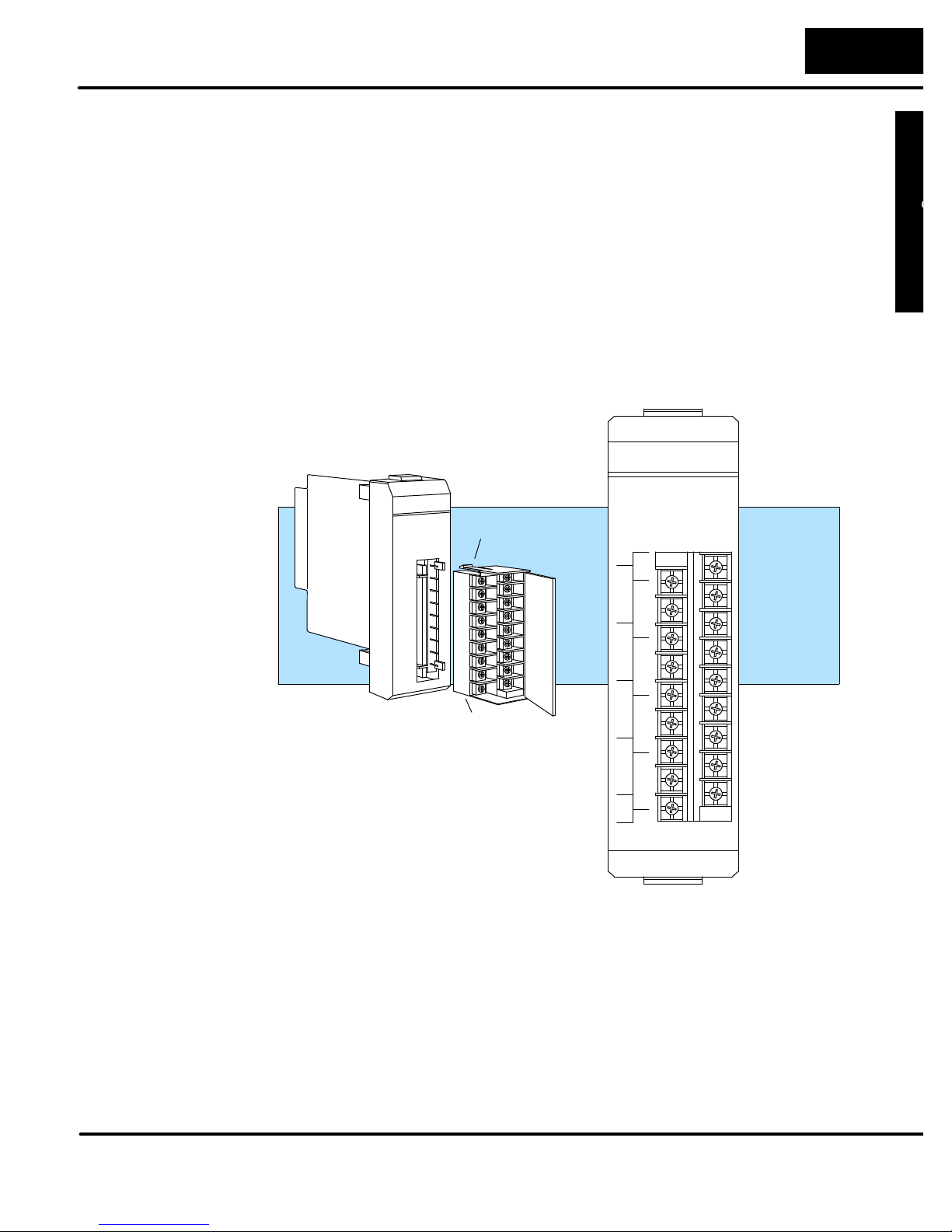
The DL305 Analog Modules provide many features thatmake the modules easier to
use. For example, the terminal block can be removed making wiring a simple task.
You can also use our DINnector product line to organize your wiring even further
(see our catalog for details).
Some of the modules provide LEDs used to determine the signal level. Since there
are not enough LEDs to show all of the channels at once, there is a small switch
underneath the terminal cover that allows you to select the channel for monitoring.
Not all of the modules have this feature.
Most of the modules also have jumpersthat can be set to select between the various
types of signals. Each chapter will show how to set these jumpers for the selections
you need.
Getting Started
ANALOG OUTPUT
F3-- 04DA--1
Squeeze Tab
Squeeze Tab
+I
CH1
--I
+I
CH3
--I
+V
CH1
--V
+V
CH3
--V
C
O
M
+I
CH2
--I
+I
CH4
--I
+V
CH2
--V
+V
CH4
--V
C
O
M
Page 16
1--
6
Getting Started
Selecting the Appropriate Module
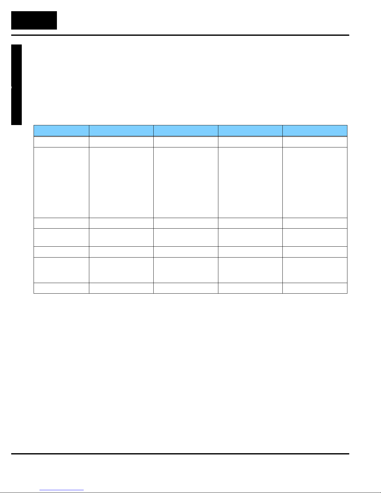
The following tables provide a condensed version of the information you need to
select the appropriate module. The most important thing is to simply determine the
number of channels required and the signal ranges that must be supported. Once
you’ve determined these parameters, look in the specific chapter for the selected
module to determine the installation and operation requirements.
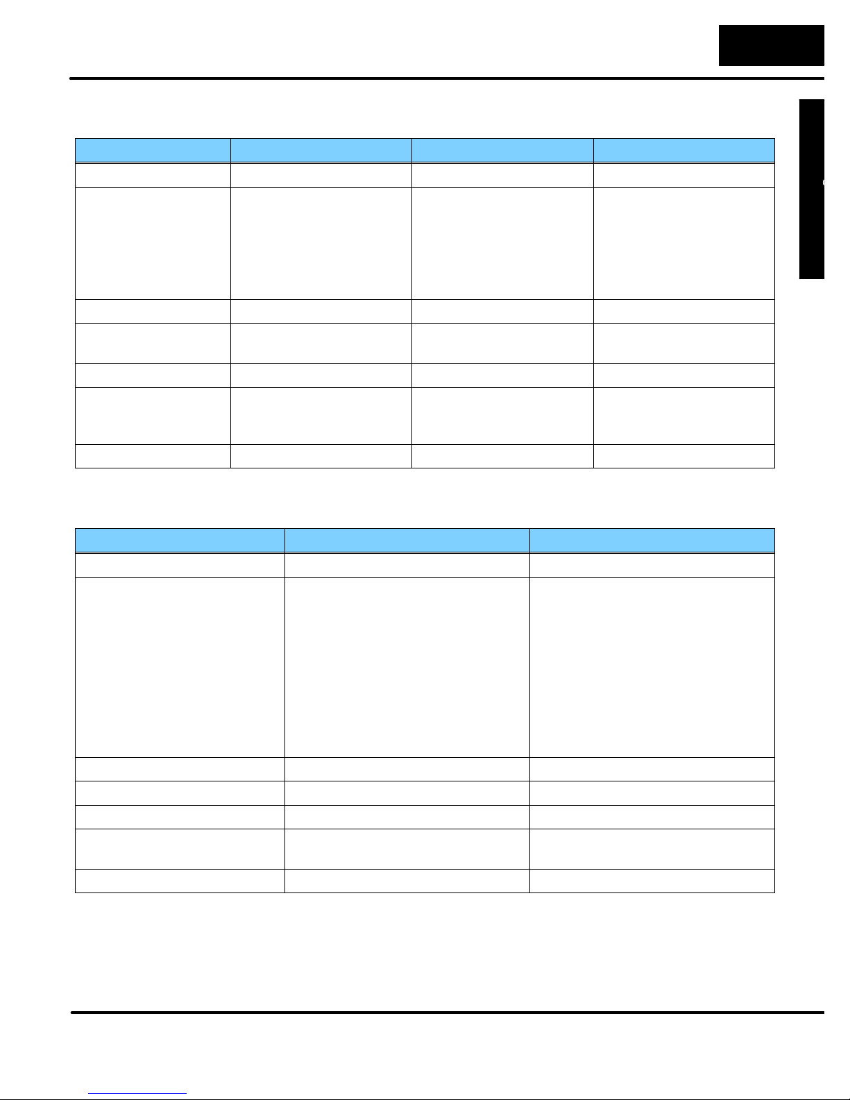
Analog Input
Specification D3--04AD F3--04ADS F3--08AD F3--16AD
Channels 4 4 8 16
Input Ranges 1 -- 5V
4 -- 20 mA
Resolution 8 bit (1 in 256) 12 bit (1 in 4096) 12 bit (1 in 4096) 12 bit (1 in 4096)
Channel
Isolation
Input Type Differential Differential Single ended Single ended
Maximum
Inaccuracy at
77 °F (25 °C)
See Chapter . . . 2 3 4 5
1
-- resolution is reduced with 4--20 mA signals. You should use the F3--08AD if the primary
application requires 4--20 mA signals.
Non-isolated
(one common)
1% ? 0.3% 0.35% 0.25% voltage
0 -- 5V
1 -- 5V
0 -- 10V
? 5V
? 10V
0 -- 20mA
4 -- 20mA
Isolated Non-isolated
4 -- 20mA 0 -- 5V
(one common)
1 -- 5V
0 -- 10V
? 5V
? 10V
0 -- 20mA
4 -- 20mA
Non-isolated
(one common)
1.25% current
1
Page 17
G
e
t
t
i
n
g
S
t
a
r
t
e
d
1--
7
Getting Started
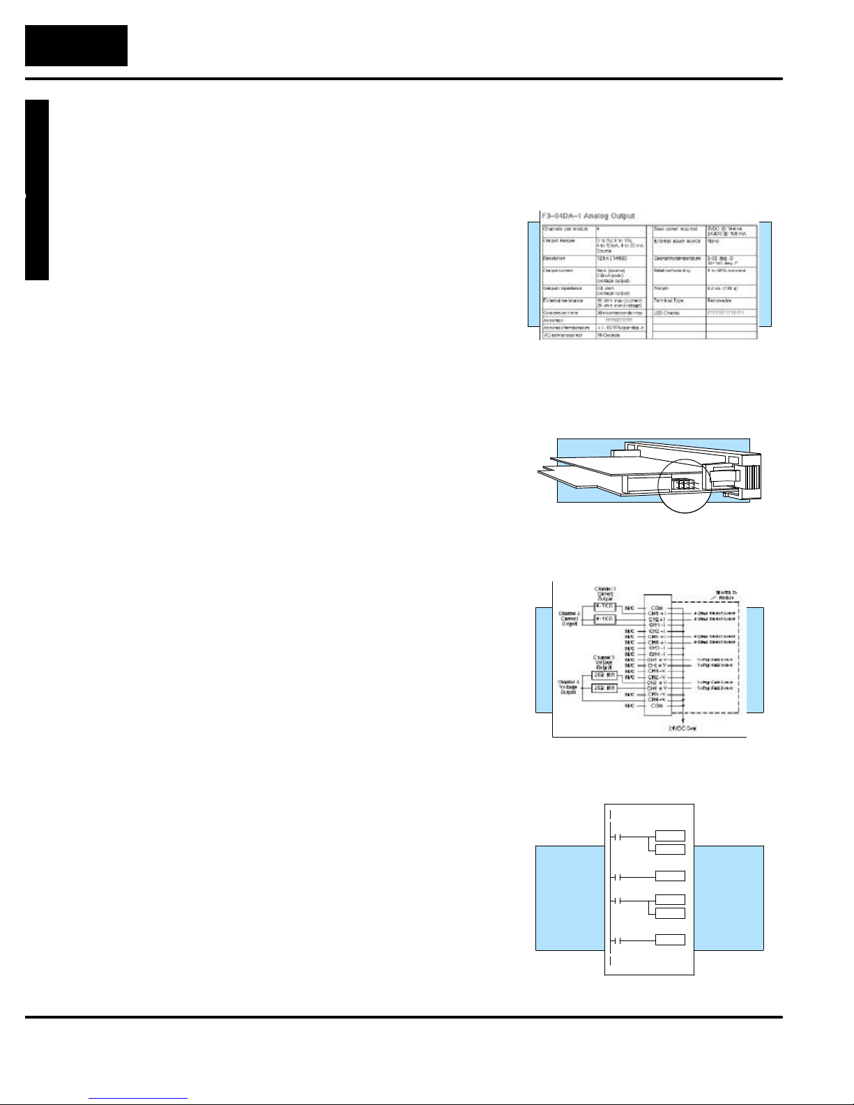
Analog Output
Specification D3--02DA FACTS F3--04DA--1 FACTS F3--04DAS
Channels 2 4 4
Output Ranges 1 -- 10VDC
4 -- 20 mA
Resolution 8 bit (1 in 256) 12 bit (1 in 4096) 12 bit (1 in 4096)
Channel Isolation Non-isolated
(one common)
Output Type Single ended Single ended Differential
Maximum
Inaccuracy at 77 °F
(25 °C)
See Chapter . . . . 6 7 8
Special Input
Specification F3--08TEMP FACTS F4--04DA
Channels 8, Temperature Input 8, Thermocouple Input
Input Ranges 0 -- 1mA
Resolution 12 bit (1 in 4096) 12 bit (1 in 4096)
? 0.4% ? 0.2% voltage
AD590 input types
0 -- 5V
0 --10V
4 -- 12mA
4 -- 20mA
Non-isolated
(one common)
? 0.6% current
0 -- 5V
0 -- 10V
? 5V
? 10V
4 -- 20mA
Isolated
? 0.8%
E: --270/1000 _C, --450/1832 _F
J: --210/760 _C, --350/1390 _F
K: --270/1370 _C, --450/2500 _F
R: 0/1768 _C, --32/3214 _F
S: 0/1768 _C, --32/3214 _F
T: --270/400 _C, --450/752 _F
50mV: 0 -- 50 mV
100mV: 0--100 mV
Channel Isolation Non-isolated Non-isolated
Input Type Single ended Differential
Maximum Inaccuracy at
77 °F (25 °C)
See Chapter . . . . 10 9
0.25% 0.35%
Page 18
1--
8
Getting Started
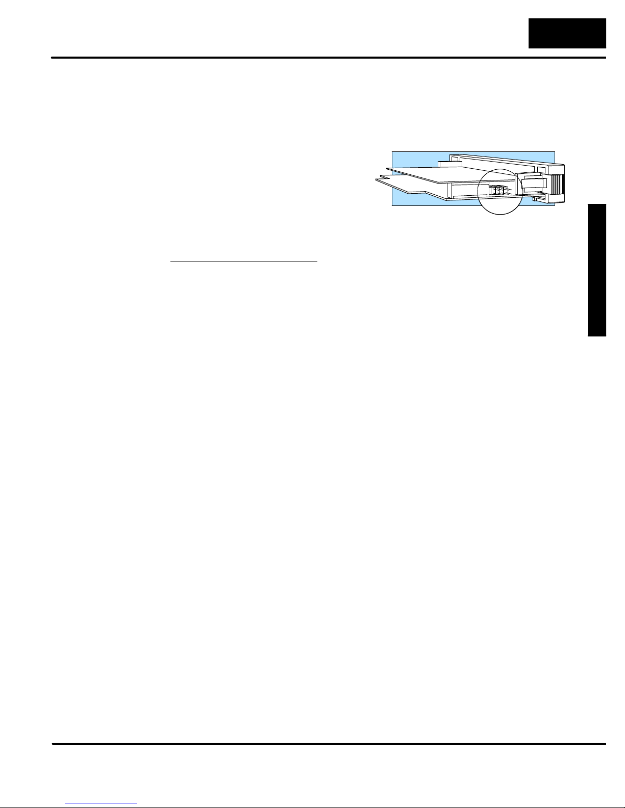
Analog Made Easy -- Four Simple Steps
Once you’ve selected the appropriate
module, use the chapter thatdescribes the
module and complete the following steps.
STEP 1. Take a minute to review the
detailed specifications to make
sure the module meets your
application requirements.
STEP 2. Set the module switches and/or
jumpers to select:
S number of channels
S the operating ranges
(voltage or current)
Note, some of the modules may
not have switches.
STEP 3. Connect the field wiring to the
module connector.
STEP 4. Review the module operating
characteristics and write the
control program.
Read the
input data
Store input
data
Calculate output
values
Write output
values
Page 19

G
e
t
t
i
n
g
S
t
a
r
t
e
d
1--
9
Analog Input Terminology
We use several different terms throughout the rest of this manual. You don’t have to
be an expert on analog terms to use the products, but it may help make it easier to
select the appropriate modules if you take a few minutes to review these definitions.
Channels per
Module
The number of analog channels or points available in the module to connect to field
devices.
Getting Started
Input Ranges
Resolution
Input Type
Input Impedance
Conversion
Method
Conversion Time
Linearity Error and
Total Tolerance
(Relative Accuracy)
Accuracy vs.
Temperature
LED Display
The input ranges in voltage and/or current that the module will operate properly
within.
The number of binary weighted bitsavailable on thedigital side of themodule for use
in converting the analog value to a digital value.
Specifies if the module accepts single ended, bipolar or differential input signals.
The input impedance of the module using a voltage or current input signal.
The method the module uses to convert the analog signal to a digital value.
The amount of time required to complete the analog to digital conversion.
The linearity and accuracy of the digital representation over the entire input range.
The effect of temperature on the accuracy of the module.
LED indicators on the module
I/O Points Required
External Power
Source
Base Power
Required
Operating
Temperature
Relative Humidity
Terminal Type
Weight
The number of I/O points the CPU must dedicate to the module.
Some modules require a separate 24VDC power source. The 24VDC output supply
at the local or expansion base can be used as long as you do not exceed the current
rating.
The amount of base current required by the module. Use this value in your power
budget calculations.
The minimum and maximum temperatures the module will operate.
The minimum and maximum humidity the module will operate.
Indicates whether the terminal type is a removable or non-removable connector or a
terminal.
The weight of the module.
Page 20

1--10
Getting Started
Analog Output Module Terminology
Channels per
Module
Output Ranges
Resolution
Output Current
Output Impedance
Load Impedance
Conversion Time
Accuracy
Accuracy vs.
Temperature
The number of analog channels or points available in the module to connect to field
devices.
The output ranges in voltage and/or current modes the module will operate properly
within.
The number of binary weighted bitsavailable on thedigital side of themodule for use
in converting the digital value to a analog signal.
The maximum current the module will drive using a voltage output signal.
The output impedance of the module using a voltage output signal.
The minimum and maximum resistance the module can drive using a current output
signal.
The amount of time required to complete the digital to analog conversion.
The linearity and calibrated accuracy of the digital representation over the entire
output range.
The effect of temperature on the accuracy of the module.
LED Display
External Power
Source
Base Power
Required
Operating
Temperature
Relative Humidity
Terminal Type
Weight
I/O Points Required
LED indicators on the module
Some modules require a separate 24VDC power source. The 24VDC output supply
at the local or expansion base can be used as long as you do not exceed the current
rating.
The amount of base current required by the module. Use this value in your power
budget calculations.
The minimum and maximum temperatures the module will operate.
The minimum and maximum humidity the module will operate.
Indicates whether the terminal type is a removable or non-removable connector or a
terminal.
The weight of the module.
The number of I/O points the CPU must dedicate to the module.
Page 21

1
2
D3--04AD
4-Channel
Analog Input
In This Chapter. . . .
— Module Specifications
— Setting the Module Jumpers
— Connecting the Field Wiring
— Module Operation
— Writing the Control Program
Page 22

4-ChannelAnalogInpu
t
2--
2
D3--04AD 4-Channel Analog Input
Module Specifications
The following table provides the specifications for the D3--04AD Analog Input
Module. Review these specifications to make sure the module meets your
application requirements.
Number of Channels 4
Input Ranges 1 -- 5V, 4 -- 20 mA
Resolution 8 bit (1 in 256)
Channel Isolation Non-isolated (one common)
Input Type Differential or Single ended
Input Impedance 1 MO minimum, voltage
Absolute Maximum Ratings 0 -- +10V maximum, voltage
Linearity ? 0.8% maximum
250O current
0 -- 30 mA maximum, current
Analog Input
Configuration
Requirements
Accuracy vs. Temperature
Maximim Inaccuracy
Conversion Method Sequential comparison
Conversion Time 2 ms maximum
Power Budget Requirement 55 mA @ 9V
External Power Supply 24 VDC, ? 10%, 65 mA, class 2
Operating Temperature
Storage Temperature
Relative Humidity 5 to 95% (non-condensing)
Environmental air No corrosive gases permitted
Vibration MIL STD 810C 514.2
Shock MIL STD 810C 516.2
Noise Immunity NEMA ICS3--304
Noise Rejection Ratio Normal mode: --6 dB/250Hz
The D3--04AD Analog Input appears as a 16-point module. The module can be
installed in any slot configured for 16 points. See the DL305 User Manual for details
on using 16 point modules in DL305 systems. The limitation onthe number ofanalog
modules are:
S For local and expansion systems, the available power budget and
16-point module usage are the limiting factors.
? 70 ppm / _C maximum
1% maximum at 25_ C
32° to 140° F (0° to 60_ C)
--4° to 158° F (--20° to 70_ C)
Common mode: 60dB/60Hz (--5 to 10V)
Page 23
D
3
-
-
0
4
A
D
4
-
C
hanne
l
A
n
alo
gInpu
t
2--
3
Setting the Module Jumpers
Therearefourjumperslocatedonthe
module that select between 1--5V and
4--20 mA signals. The module is shipped
from the factory for use with 1--5V
signals.
If you want to use 4 -- 20 mA signals, you
have to install a jumper. No jumper is
required for 1 -- 5V operation. Each
channel range may be selected
independently of the others.
Range Jumper
1 -- 5V Removed
4 -- 20 mA Installed
D3--04AD 4-Channel Analog Input
Connecting the Field Wiring
Wiring Guidelines
User Power Supply
Requirements
Your company may have guidelines for wiring and cable installation. If so, you should
check those before you begin the installation. Here are some general things to
consider.
S Use the shortest wiring route whenever possible.
S Use shielded wiring and ground the shield at the signal source. Do not
ground the shield at both the module and the source.
S Don’t run the signal wiring next to large motors, high current switches, or
transformers. This may cause noise problems.
S Route the wiring through an approved cable housing to minimize the risk
of accidental damage. Check local and national codes to choose the
correct method for your application.
The D3--04AD requires a separate power supply. The DL305 bases have built-in 24
VDC power supplies that provide up to 100 mA of current. If you only have one
analog module, you can use this power source instead of a separate supply. If you
have more than two analog modules, or you would rather use a separate supply,
choose one that meets the following requirements: 24 VDC ? 10%, Class 2, 65mA
current (or greater, depending on the number of modules being used.)
Page 24
4-ChannelAnalogInpu
t
2--
4
D3--04AD 4-Channel Analog Input
Custom Input
Ranges
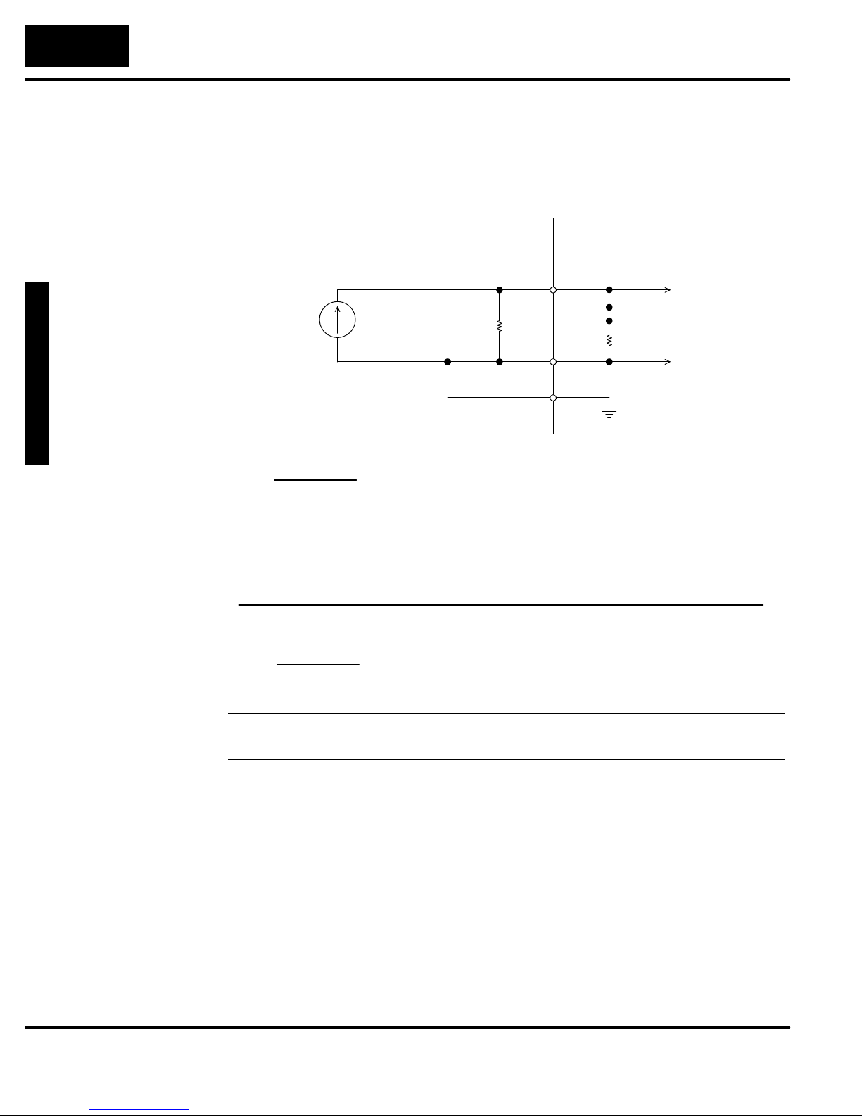
Occasionally you may have the need to connect a transmitter with an unusual signal
range. By changing the wiring slightly and adding an external resistor to convert the
current to voltage, you can easily adapt this module to meet the specifications for a
transmitter that does not adhere to one of the standard input ranges. The following
diagram shows how this works.
Internal
Module
Circuitry
Removed
+
Jumper
250O
--
V
max
+
(single ended)
--
Field wiring
50mA
Current
transmitter
+ch1
R
-- ch1
0V
R =
I
max
R = value of external resistor
V
= high limit of selected voltage range
max
I
= maximum current supplied by the transmitter
max
Example: current transmitter capable of 50mA, 1 -- 5V range selected.
5V
R =
R = 100 ohms
50mA
NOTE: Your choice of resistor can affect the accuracy of the module. A resistor that
has ? 0.1% tolerance and a ? 50ppm / _C temperature coefficient is recommended.
Page 25
D
3
-
-
0
4
A
D
4
-
C
hanne
l
A
n
alo
gInpu
t
2--
5
D3--04AD 4-Channel Analog Input
Current Loop
Transmitter
Impedance
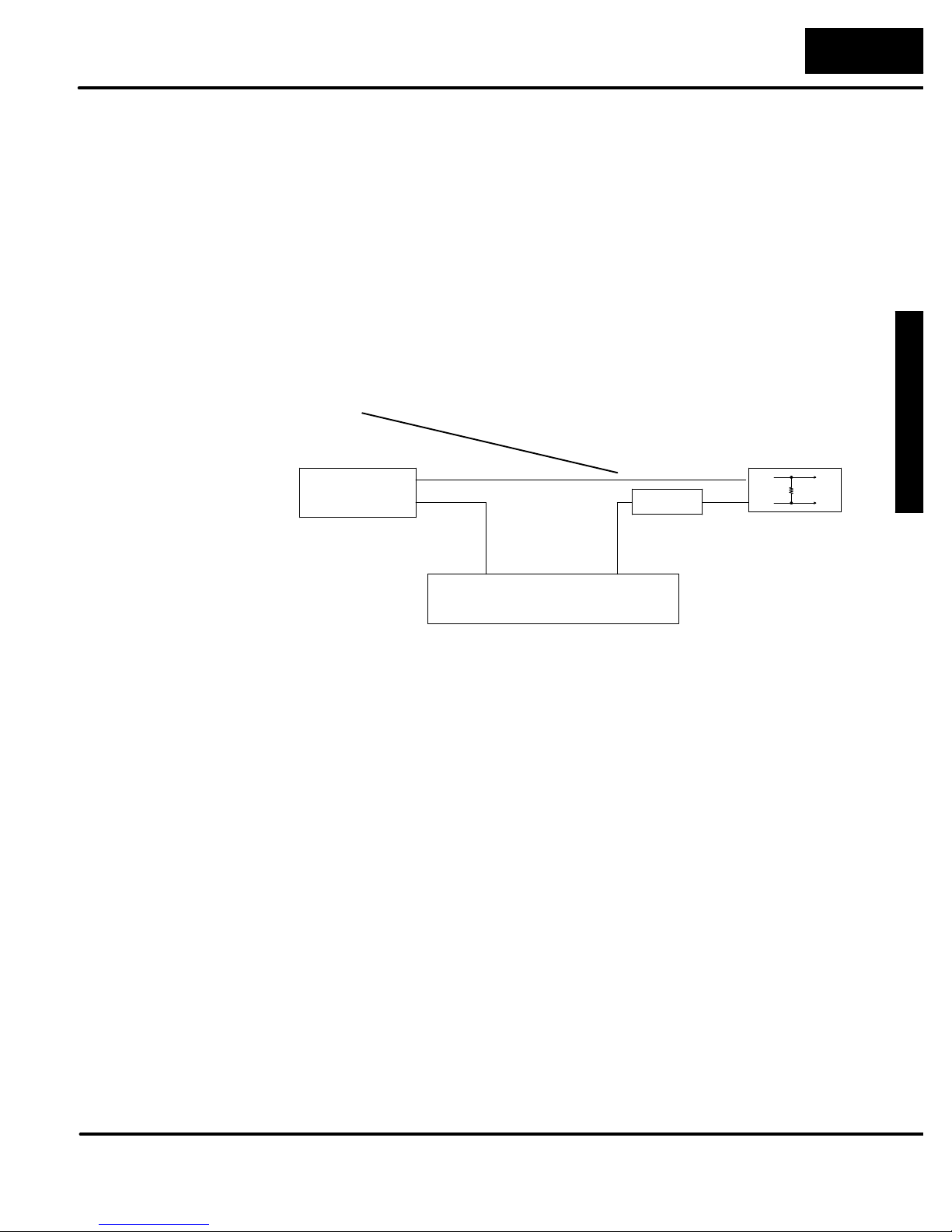
Standard 4 to 20 mA transmitters and transducers can operate froma wide variety of
power supplies. Not all transmitters are alike and the manufacturers often specify a
minimum loop or load resistance that must be used with the transmitter.
The D3--04AD provides 250 ohm resistance for each channel. If your transmitter
requires a load resistance below 250 ohms, then you do not have to make any
adjustments. However, if your transmitter requires a load resistancehigher than 250
ohms, then you need to add a resistor in series with the module.
Consider the following example for a transmitter being operated from a 36 VDC
supply with a recommended load resistance of 750 ohms. Since the module has a
250 ohm resistor, you need to add an additional resistor.
R = Tr -- Mr
R = 750 -- 250
R ² 500
DC Supply
0V
+36V
R -- Resistor to add
Tr -- Transmitter Requirement
Mr -- Module resistance (internal 250 ohms)
Module Channel 1
R
-+
250O
+ --
Two-wire Transmitter
Page 26
4-ChannelAnalogInpu
t
2--
6
D3--04AD 4-Channel Analog Input
Removable
Connector
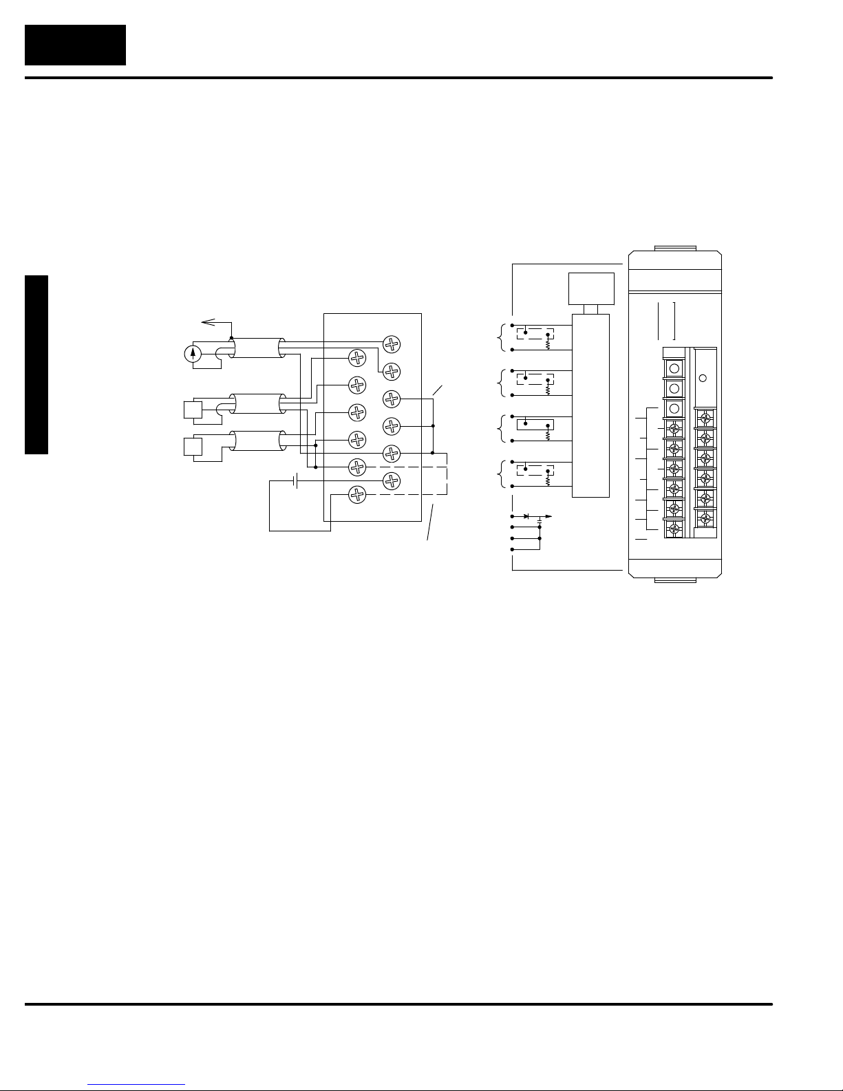
The D3--04AD module has a removable connector to make wiring easier. Simply
squeeze the tabs on the top and bottom and gently pull the connector from the
module.
Wiring Diagram
Note 1: Terminate all shields of the cable at their respective
signal source.
Note 2: Unused channels should be shorted to 0V or have the
Jumper installed for current input for best noise immunity.
Note 3: When a differential input is not used 0V should be
connected to the -- of that channel.
See Note 1
CH3 Differential
Current Transmitter
CH1 Differential
Voltage Transmitter
CH2 Single-ended
Voltage Transmitter
+
OV
--
+
OV
--
+
--
-- +
24VDC
1
2
Internal
Module
Wiring
A--D
Convertor
+
Analog
+
+
3
--
Used
--
+
--
0V
0
V
See Note 2
+
4
--
0
V
+24
V
Internally
Connected
CH4
Not
CH1
CH2
CH3
CH4
+24VDC
0V
0V
0V
250
250
250
250
--
+
--
+
--
+
--
Internal
Circuitry
Switch
ANALOG INPUT
D3--04AD
1
1
1
CH DSPY
CH
DSPY
SEL
+
1
--
+
2
--
0
V
0
V
16
2
2
2
32
3
3
4
64
4
4
8
128
+
3
--
+
4
--
0
V
24
V
Page 27
D
3
-
-
0
4
A
D
4
-
C
hanne
l
A
n
alo
gInpu
t
2--
7
Module Operation
Before you begin writing the control program, it is important to take a few minutes to
understand how the module processes and represents the analog signals.
Channel Scanning
Sequence
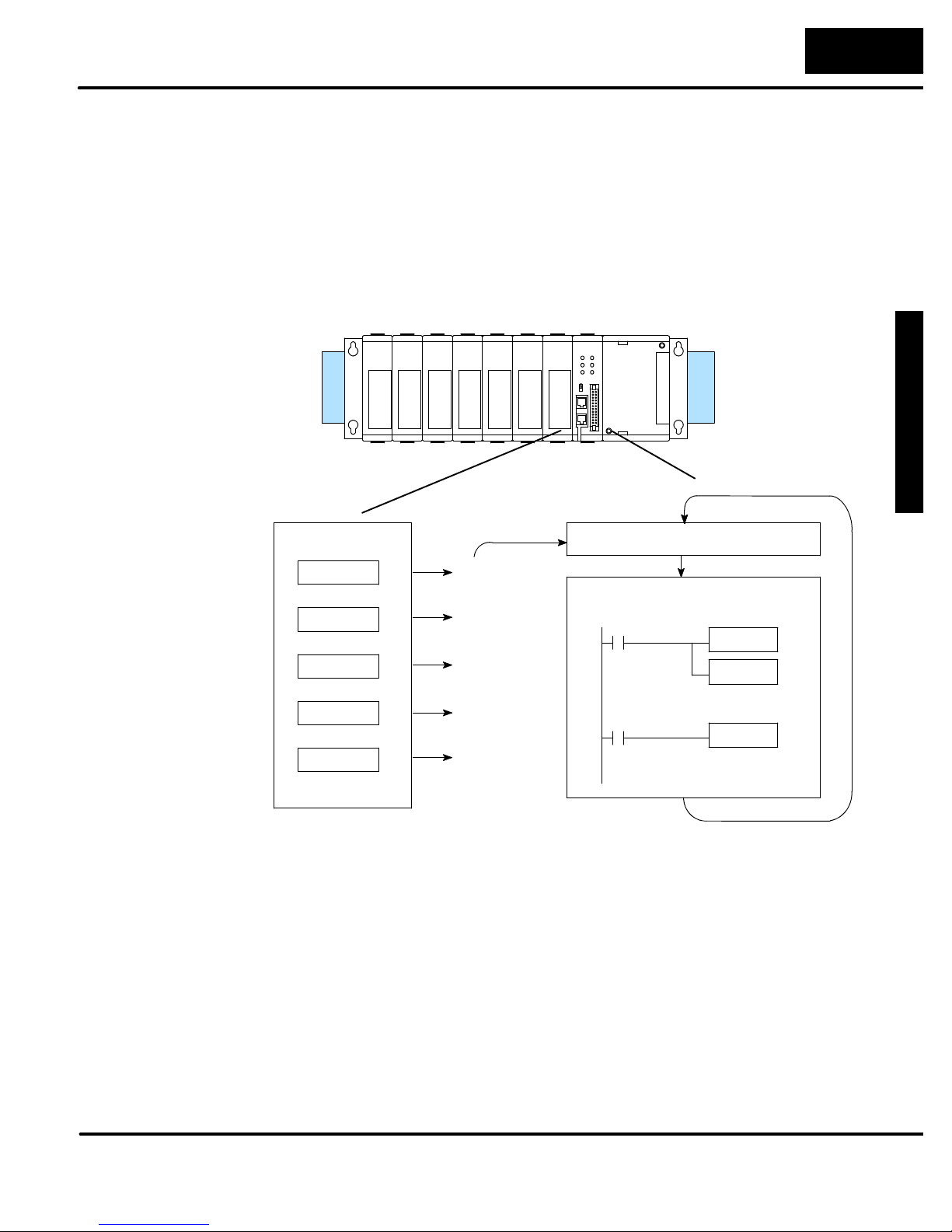
The D3--04AD module supplies 1 channel of data per each CPU scan. Since there
are four channels, it can take up to four scans to get data for all channels. Once all
channels have been scanned, the process starts over with channel 1.
You do not have to select all of the channels. Unused channels are not processed, so
if you select only two channels, then each channel will be updated every other scan.
D3--04AD 4-Channel Analog Input
Scan
I/O Update
Channel 1
Scan N
Execute Application Program
Channel 2
Channel 3
Channel 4
Channel 1
Scan N+1
Scan N+2
Scan N+3
Scan N+4
Read the data
Store data
Even though the channel updates to the CPU are synchronous with the CPU scan,
the module asynchronously monitors the analog transmitter signal and converts the
signal to a 8-bit binary representation. This enables the module to continuously
provide accurate measurements without slowing down the discrete control logic in
the RLL program.
Page 28
4-ChannelAnalogInpu
t
2--
8
D3--04AD 4-Channel Analog Input
Understanding the
I/O Assignments
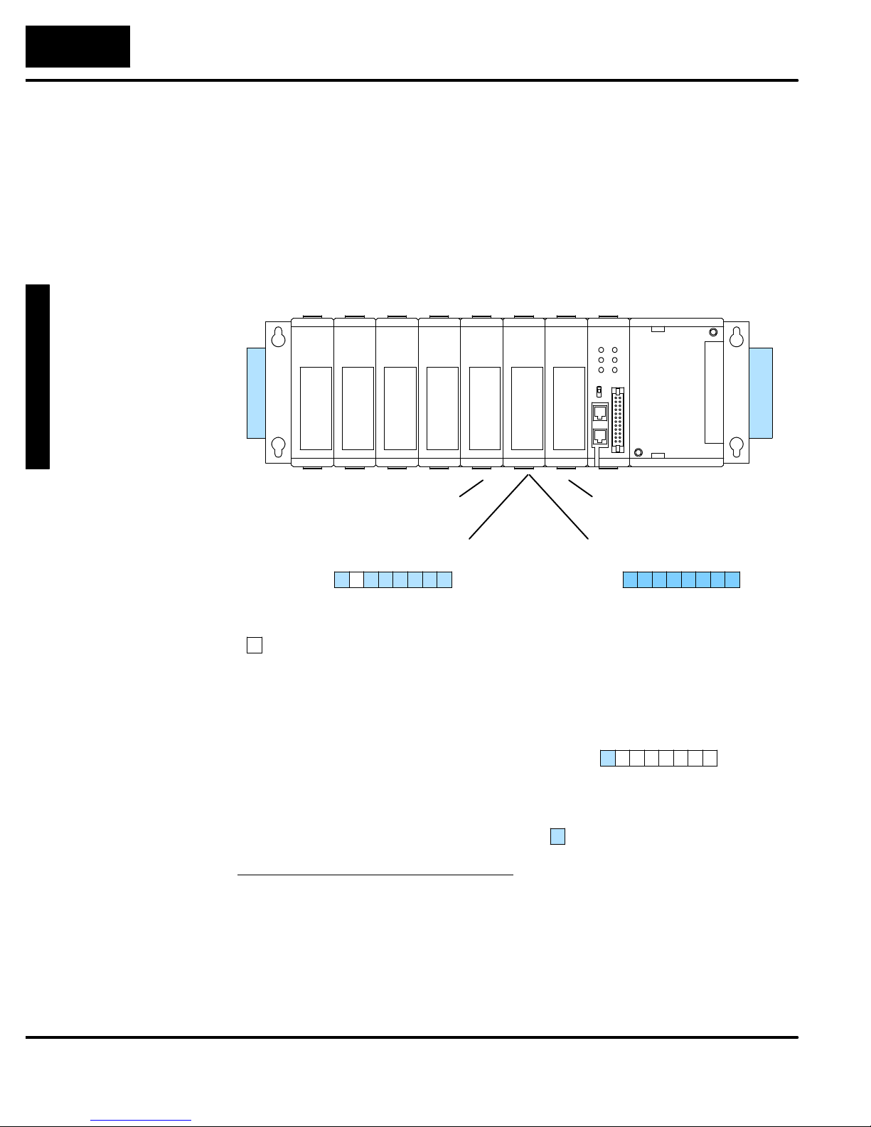
You may recall the D3--04AD module appears to the CPU as a 16-point module.
Some of the points are inputs to the CPU and some are outputs to the module. These
16 points provide:
S an indication of which channel is active.
S the digital representation of the analog signal.
Since all I/O points are automatically mapped into Register (R) memory, it is very
easy to determine the location of the data word that will be assigned to the module.
D3--04AD
8pt
Relay
050
057
8pt
Output
Output
040
--
--
047
R 002, R012 R 000, R010
8pt
030
--
037
16pt
Input
020
027
-120
127
4ch.
(Analog)
010
017
-110
117
16pt
Input
000
007
100
107
--
All Channel
Scan Output
R 011
MSB LSB
1
1
7
1
1
0
MSB LSB
R 001
0
1
7
0
1
0
-- not used
Within these two register locations, the individual bits represent specific information
about the analog signal.
The most significant point (MSP)
assigned to the module acts as an output
to the module and controls the channel
MSB LSB
R011
scanning sequence. This allows
flexibility in your control program.
If this output is on, all channels will be
scanned sequentially. If the output is off,
you can use other points to select a
single channel for scanning.
1
1
1
1
1
1
1
1
1
1
7
6
5
4
3
-- scan all channels
1
1
1
1
1
1
0
2
1
Scan Out 117 Channel Input
N Off None
N+1 On 1
N+2 On 2
N+3 On 3
N+4 On 4
N+5 On 1
N+6 Off None
N+7 Off None
Page 29
D
3
-
-
0
4
A
D
4
-
C
hanne
l
A
n
alo
gInpu
t
2--
9
D3--04AD 4-Channel Analog Input
Single Channel
Scan Outputs
Active Channel
Selection Inputs
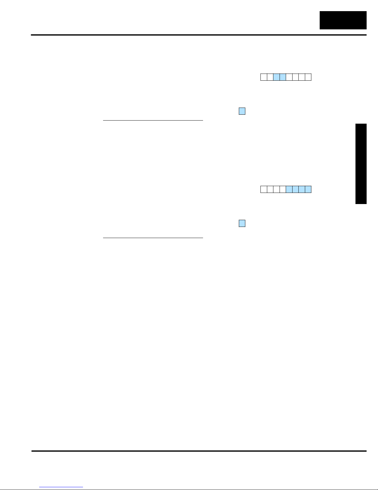
The upper register also contains two
additional outputs that can be used to
choose a single channel for scanning.
These outputs are ignored if the channel
scan output is turned on.
(Note, our example shows outputs 114
and 115. Your output point will depend on
where you have installed the module.)
Out 114 Out 115 Channel
Off Off 1
On Off 2
Off On 3
On On 4
The first four points of the upper register
are used as inputs to tell the CPU which
channel is being processed.
(Remember, the previous bits only tell
the module which channels to scan.) In
our example, when input 110 is on the
module is telling the CPU it is processing
channel 1. Here’s how the inputs are
assigned.
Input Active Channel
110 1
111 2
112 3
113 4
R011
MSB LSB
1
1
1
1
1
1
1
1
1
1
7
6
5
4
3
1
1
1
1
1
1
0
2
1
-- scan a single channel
R011
MSB LSB
1
1
1
1
1
1
1
1
1
1
7
6
5
4
3
1
1
1
1
1
1
0
2
1
-- channel selection inputs
Page 30
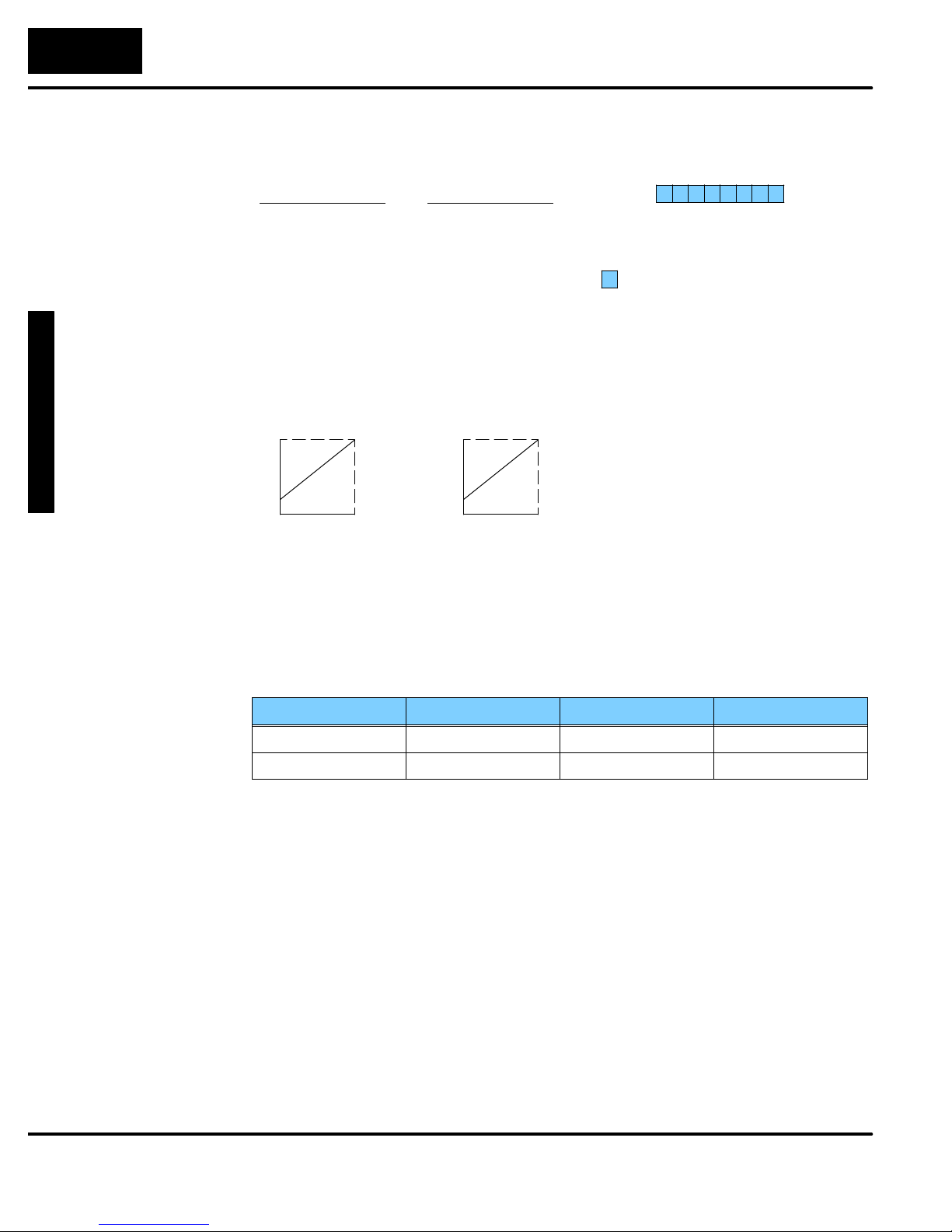
4-ChannelAnalogInpu
t
2--10
D3--04AD 4-Channel Analog Input
Analog Data Bits
The first register contains 8 bits which
represent the analog data in binary
format.
MSB LSB
R001
Bit Value Bit Value
0 1 4 16
1 2 5 32
2 4 6 64
3 8 7 128
0
1
7
-- analog data bits
0
1
0
Since the module has 8-bit resolution, the analog signal is converted into 256
“pieces” ranging from 0 -- 255 (28). For example, with a 1 to 5V scale, a 1V signal
would be 0, and a 5V signal would be 255. This is equivalent to a a binary value of
0000 0000 to 1111 1111, or 00 to FF hexadecimal. The following diagram shows how
this relates to each signal range.
1V -- 5V
+5V
1V
0 255
4 -- 20mA
20mA
4mA
0 255
Each “piece” can also be expressed in
terms of the signal level by using the
Resolution = (H--L)/255
equation shown. The following table
shows the smallest signal levels that
could possibly result in a change in the
data value for each signal range.
H = high limit of the signal range
L = low limit of the signal range
Range Highest Signal Lowest Signal Smallest Change
1 to 5V 5V 1V 15.6 mV
4 to 20mA 20mA 4mA 62.7 mA
Now that you understand how the module and CPU work together to gather and
store the information, you’re ready to write the control program.
Page 31
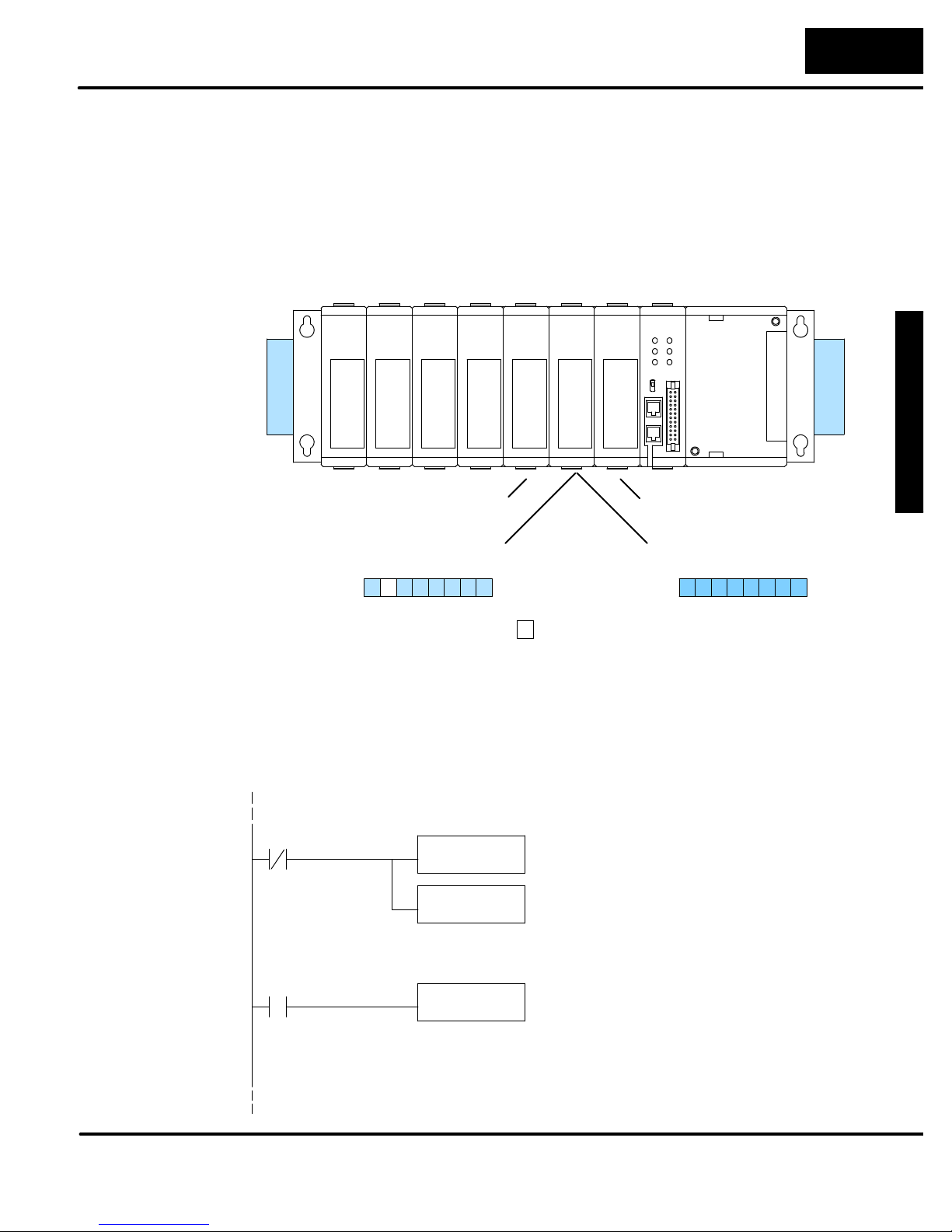
D
3
-
-
0
4
A
D
4
-
C
hanne
l
A
n
alo
gInpu
t
2--11
Writing the Control Program
D3--04AD 4-Channel Analog Input
Identifying the
Data Locations
Since all channels are multiplexed into a single data word, the control program must
be setup to determine which channel is being read. Since the module provides input
points to the CPU, it is very easy to use the channel status bits to determine which
channel is being monitored.
D3--04AD
8pt
Relay
050
057
8pt
Output
Output
040
--
--
047
R 002, R012 R 000, R010
R 011
MSB LSB
1
1
7
8pt
030
--
037
16pt
Input
020
027
120
127
(Analog)
--
4ch.
010
017
110
117
16pt
Input
000
007
--
--
100
107
R 001
MSB LSB
1
1
0
-- not used
0
1
7
0
1
0
Single Channel on
Every Scan
The following example shows a program that is designed to read a single channel of
analog data into a Register location on every scan. Once the data is in a Register,
you can perform math on the data, comparethe data againstpreset values, etc. This
example is designed to read channel 1. If you choose another channel, you would
have to add a rung (or rungs) that use the channelselect bits to select the channelfor
scanning. You would also have to change the rung that stores the data.
Read the data
374
Store channel 1
110
DSTR1
R001
BCD F86
DOUT
R400
F51
F60
This rung loads the data into the accumulator on
every scan. (You can use any permissive contact.)
The DL305 CPUs perform math operations in
BCD. This instruction converts the binary data to
BCD. (You can omit this step if your application
does not require the conversion.)
The channel selection inputs are used to let the
CPU know which channel has been loaded into the
accumulator. Channel 1 input has been used in the
example, but you could easily use a different input
for a different channel. By using these inputs to
control a DOUT instruction, you can easily move
the data to a storage register. The BCD value will
be stored in R400 and R401. (Two bytes are
required for four digit BCD numbers.)
Page 32
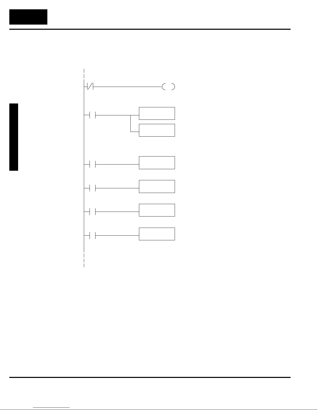
4-ChannelAnalogInpu
t
2--12
D3--04AD 4-Channel Analog Input
Reading Multiple
Channels over
Alternating Scans
The following example shows a program that is designed to read multiple channels
of analog data into Register locations. This example reads one channel per scan.
Once the data is in a Register, you can perform math on the data, compare the data
against preset values, etc.
Scan all channels
374
Read the data
117
Store channel 1
110
Store channel 2
111
117
OUT
DSTR1
R001
BCD F86
DOUT
R400
DOUT
R402
F51
F60
F60
Turn on output 117, which instructs the module to
scan all channels.
This rung loads the data into the accumulator. This
rung executes for all channels.
The DL305 performs math operations in BCD. This
instruction converts the binary data to BCD. (You
can omit this step if your application does not
require the data in BCD format.)
The channel selection inputs are used to let the
CPU know which channel has been loaded into the
accumulator. By using these inputs to control a
DOUT instruction, you can easily move the data to
a storage register. Notice that the DOUT
instruction stores the data in two bytes. (Two bytes
are required for four digit BCD numbers.)
Store channel 3
112
Store channel 4
113
DOUT
R404
DOUT
R406
F60
F60
Page 33
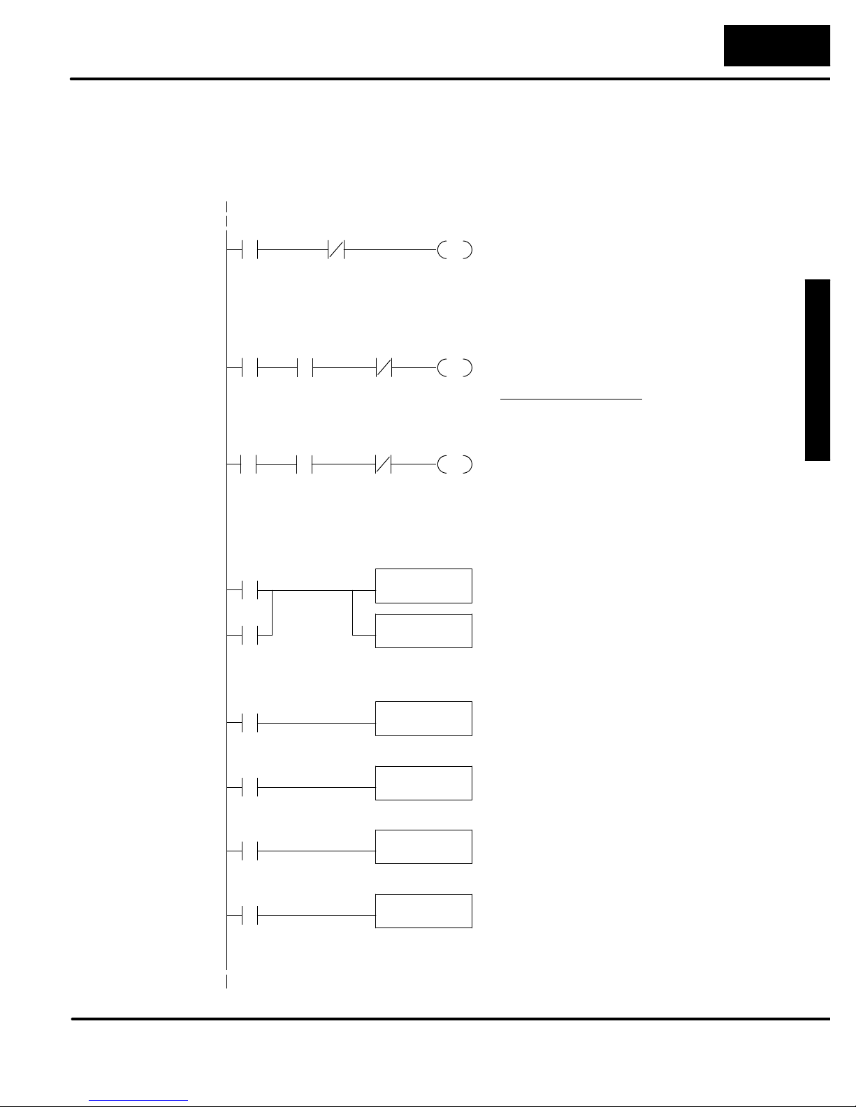
D
3
-
-
0
4
A
D
4
-
C
hanne
l
A
n
alo
gInpu
t
2--13
D3--04AD 4-Channel Analog Input
Single or Multiple
Channels
The following example shows how you can use the same program to read either all
channels or a single channel of analog data into Register locations. Once the data is
in a Register, you can perform math on the data, compare the data against preset
values, etc.
Select all channels
000
Single Channel
001
Single Channel
001
002
003
001
000
000
117
OUT
114
OUT
115
OUT
Inputs 000 and 001 are used to select between
single channel scanning and all channel scanning.
These two points were arbitrarily chosen and could
be any permissive contacts. When output 117 is
on, all channels will be scanned.
Input 001 selects single channel scan. Inputs 002
and 003 select which channel by turning on
outputs 114 and 115 as necessary.
114 115 Channel
Off Off Ch. 1
On Off Ch. 2
Off On Ch. 3
On On Ch. 4
Read the data
000
001
Store channel 1
110
Store channel 2
111
Store channel 3
112
Store channel 4
113
DSTR1
R001
BCD F86
DOUT
R400
DOUT
R402
DOUT
R404
DOUT
R406
F51
F60
F60
F60
F60
This rung loads the data into the accumulator. This
rung executes for all channel scan or single
channel scan.
The DL305 performs math operations in BCD. This
instruction converts the binary data to BCD. (You
can omit this step if your application does not
require the data in BCD format.)
The channel selection inputs are used to let the
CPU know which channel has been loaded into the
accumulator. By using these inputs to control a
DOUT instruction, you can easily move the data to
a storage register. Notice that the DOUT
instruction stores the data in two bytes. This is
because two bytes are required to store the BCD
number.
Page 34

4-ChannelAnalogInpu
t
2--14
D3--04AD 4-Channel Analog Input
Thefollowingexampleshowshowyo
u
Scaling the Input
Data
Most applications usually require
measurements in engineering units,
which provide more meaningful data.
This is accomplished by using the
conversion formula shown.
would use the analog data to represent
pressure (PSI) from 0 to 100. This
example assumes the analog value is
110, which is slightly less than half scale.
This should yield approximately 42.9
PSI.
Units = (A/256)*S
Units = value in Engineering Units
A = Analog value (0 -- 255)
S = high limit of the Engineering
unit range
Units = (A/256)*S
Units = (110/256)*100
Units = 42.9
Page 35
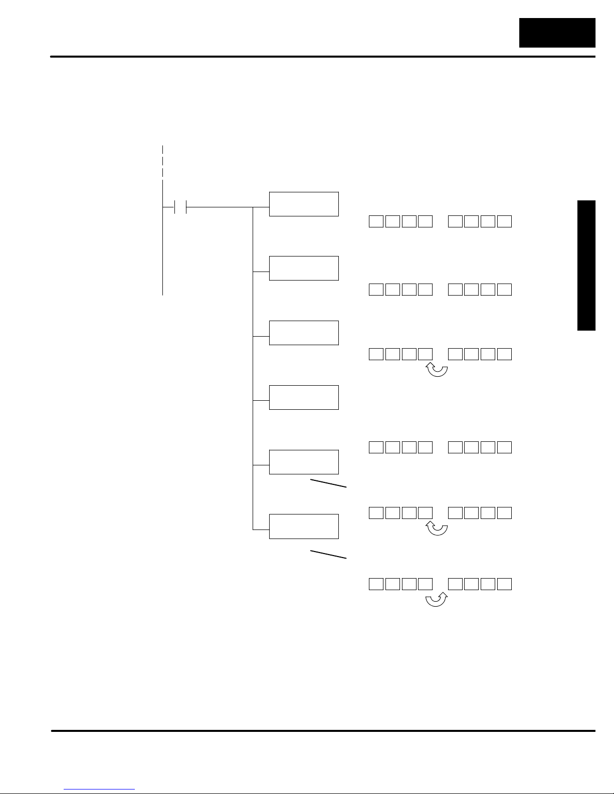
D
3
-
-
0
4
A
D
4
-
C
hanne
l
A
n
alo
gInpu
t
2--15
D3--04AD 4-Channel Analog Input
The following instructions are required to scale the data. We’ll continue to use the
42.9 PSI example. In this example we’re using channel 1. Input 110 is the active
channel indicator for channel 1. Of course, if you were using a different channel, you
would use the active channel indicator point that corresponds to the channel you
were using.
This example assumes you have already read the analog data
and stored the BCD equivalent in R400 and R401
Scale the data
110
DSTR
R400
F50
This instruction brings the analog value (in BCD)
into the accumulator.
Accumulator
0 1 1 0
Aux. Accumulator
0 0 0 0
R577 R576
DIV
K256
DSTR
R576
MUL
K100
DSTR
R576
DOUT
R450
F74
F50
F73
F50
F60
The analog value is divided by the resolution of the
module, which is 256. (110 / 256 = 0.4296)
Accumulator
0 0 0 0
This instruction moves the two-byte decimal
portion into the accumulator for further operations.
Accumulator
4 2 9 6
The accumulator is then multiplied by the scaling
factor, which is 100. (100 x 4296 = 429600). Notice
that the most significant digits are now stored in
the auxilliary accumulator. (This is different from
the way the Divide instruction operates.)
Accumulator
9 6 0 0
This instruction moves the two-byte auxilliary
accumulator for further operations.
Accumulator
0 0 4 2
This instruction stores the accumulator to R450
and R451. R450 and R451 now contain the PSI,
which is 42 PSI.
Accumulator
0 0 4 2
Aux. Accumulator
4 2 9 6
R577 R576
Aux. Accumulator
4 2 9 6
R577 R576
Aux. Accumulator
0 0 4 2
R577 R576
Aux. Accumulator
0 0 4 2
R577 R576
Store in R451 & R450
0 0 4 2
R451 R450
Page 36
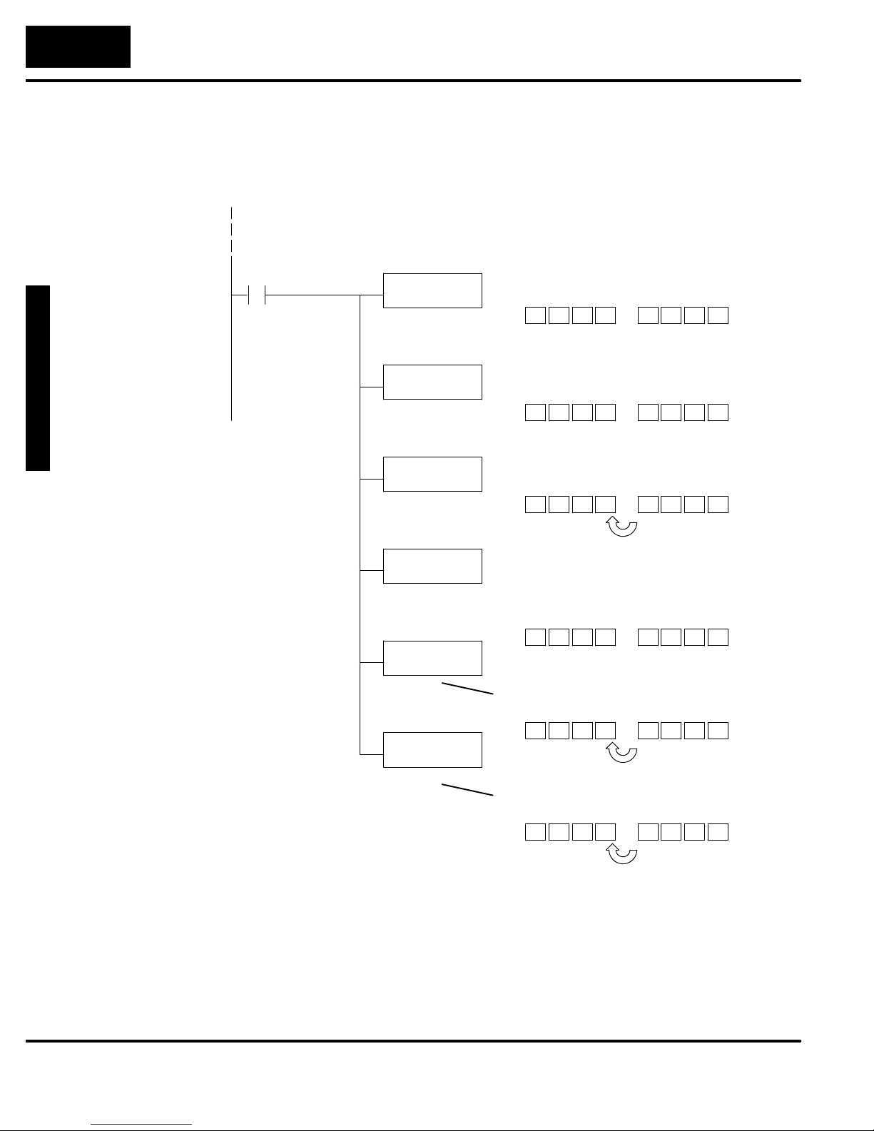
4-ChannelAnalogInpu
t
2--16
D3--04AD 4-Channel Analog Input
You probably noticed that the previous example yielded 42 PSI when the real value
should have been 42.9 PSI. By changingthe scalingvalue slightly, we can “imply” an
extra decimal of precision. Notice in the following example we’ve added another digit
to the scale. Instead of a scale of 100, we’re using 1000, which implies 100.0 for the
PSI range.
This example assumes you have already read the analog data
and stored the BCD equivalent in R400 and R401
Scale the data
110
DSTR
R400
F50
This instruction brings the analog value (in BCD)
into the accumulator.
Accumulator
0 1 1 0
Aux. Accumulator
0 0 0 0
R577 R576
DIV
K256
DSTR
R576
MUL
K1000
DSTR
R576
DOUT
R450
F74
F50
F73
F50
F60
The analog value is divided by the resolution of the
module, which is 256. (110 / 256 = 0.4296)
Accumulator
0 0 0 0
This instruction moves the two-byte decimal
portion into the accumulator for further operations.
Accumulator
4 2 9 6
The accumulator is multiplied by the scaling factor,
which is now 1000. (1000 x 4296 = 4296000). The
most significant digits are now stored in the
auxilliary accumulator. (This is different from the
way the Divide instruction operates.)
Accumulator
6 0 0 0
This instruction moves the two-byte auxilliary
accumulator for further operations.
Accumulator
0 4 2 9
Aux. Accumulator
4 2 9 6
R577 R576
Aux. Accumulator
4 2 9 6
R577 R576
Aux. Accumulator
0 4 2 9
R577 R576
Aux. Accumulator
0 4 2 9
R577 R576
This instruction stores the accumulator to R450.
R450 now contains the PSI, which implies 42.9.
Accumulator
0 4 2 9
Store in R451 & R450
0 4 2 9
R451 R450
Page 37
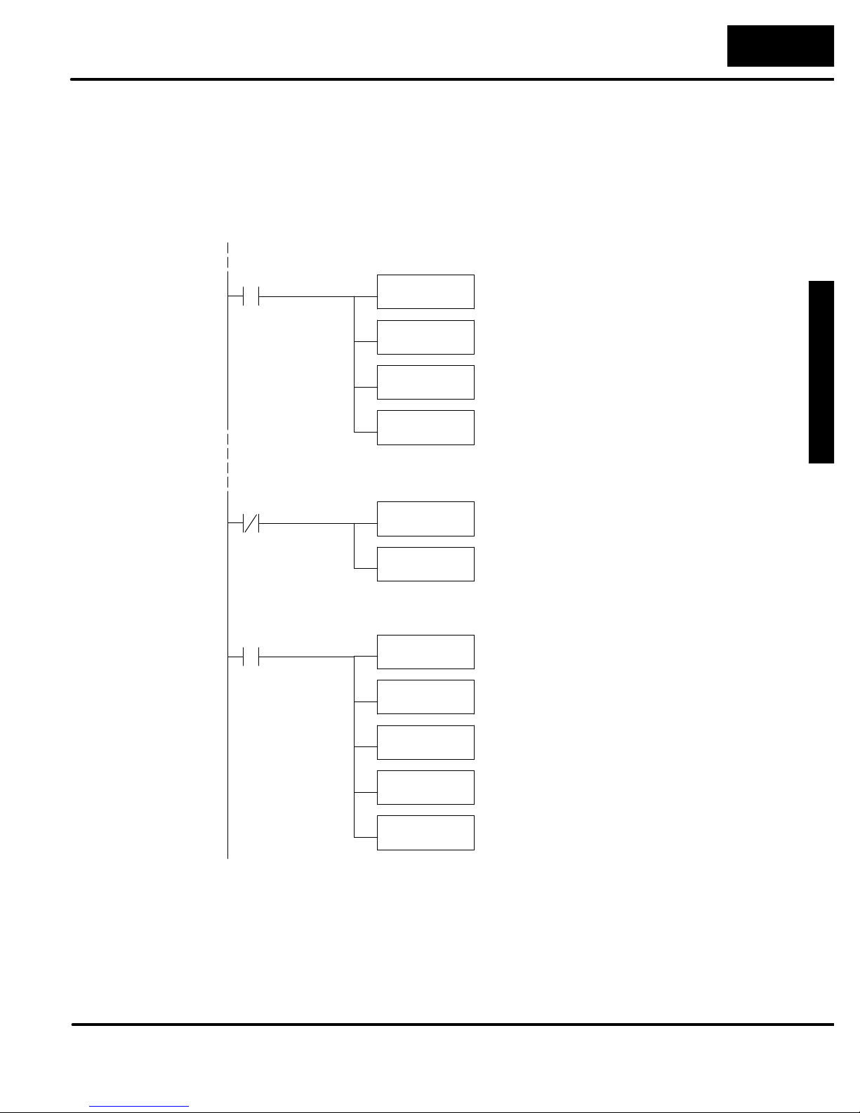
D
3
-
-
0
4
A
D
4
-
C
hanne
l
A
n
alo
gInpu
t
2--17
D3--04AD 4-Channel Analog Input
This example program shows how you can use the instructions to load the equation
constants into data registers. The example is written for channel 1, but you can
easily use a similar approach to use different scales for all channels if required.
You may just use the appropriate constants in the instructions dedicated for each
channel, but this method allows easier modifications. For example, you could easily
use an operator interface or a programming device to change the constants if they
are stored in Registers.
Load the constants
374
DSTR
K256
F50
On the first scan, these first two instructions load
the analog resolution (constant of 256) into R430
and R431.
Read the data
374
Store channel 1
110
DOUT
R430
DSTR
K1000
DOUT
R432
DSTR1
R001
BCD F86
DIV
R430
DSTR
R576
MUL
R432
F60
F50
F60
F51
F74
F50
F73
These two instructions load the high limit of the
Engineering unit scale (constant of 1000) into
R432 and R433. Note, if you have different scales
for each channel, you’ll also have to enter the
Engineering unit high limit for those as well.
This rung loads the data into the accumulator on
every scan. (You could use any permissive contact.)
The DL305 CPUs perform math operations in
BCD. Since we will perform math on the data, the
data must be converted from binary data to BCD.
The analog value is divided by the resolution of the
module, stored in R430.
This instruction moves the decimal portion from the
auxilliary accumulator into the regular accumulator
for further operations.
The accumulator is multiplied by the scaling factor,
stored in R432.
DSTR
R576
DOUT
R400
F50
F60
This instruction moves most significant digits (now
stored in the auxilliary accumulator) into the
regular accumulator for further operations.
The scaled value is stored in R400 and R401 for
further use.
Page 38
4-ChannelAnalogInpu
t
2--18
D3--04AD 4-Channel Analog Input
Analog and Digital
Value Conversions
Sometimes it is helpful to be able to quickly convert between the signal levels and the
digital values. This is especially helpful during machine startup or troubleshooting.
The following table provides formulas to make this conversion easier.
Range If you know the digital value ... If you know the analog signal
level ...
1 to 5V
4 to 20mA
A = (4D/255) + 1
A = (16D/255) + 4
D = (255/4)(A--1)
D = (255/16)(A--4)
For example, if you are using the 1 to 5V
range and you have measured the signal
D = (255/4)(A--1)
at 3V, you would use the following
formula to determine the digital value
that should be stored in the register
location that contains the data.
D = (255/4)(3V--1)
D = (63.75) (2)
D = 127.5 (or 128)
Now you have all the necessary information to get your analog module installed and
operating correctly!
Page 39

1
3
F3--04ADS
4-Channel Isolated
Analog Input
In This Chapter. . . .
— Module Specifications
— Setting the Module Jumpers
— Connecting the Field Wiring
— Module Operation
— Writing the Control Program
Page 40

4-Ch.IsolatedAnalogIn
.
3--
2
F3--04ADS 4-Channel Isolated Analog Input
Module Specifications
The following table provides the specifications for the F3--04ADS Analog Input
Module. Make sure the module meets your application requirements.
Number of Channels 4, isolated
Input Ranges 0 -- 5V, 0 -- 10V, 1 -- 5V, ? 5V, ? 10V,
Resolution 12 bit (1 in 4096)
Input Type Differential
Max. Common mode voltage ? 750V peak continuous transformer isolation
Noise Rejection Ratio Common mode: --100 dB at 60Hz
Active Low-pass Filtering --3 dB at 10Hz, --12 dB per octave
Input Impedance 250O ? 0.1%, 1/2W current input
Absolute Maximum Ratings ? 40 mA, current input ? 100V, voltage input
Conversion Time 1 channel per scan, successive
Linearity Error ? 1 count (0.03% of full scale) maximum
0 -- 20 mA, 4 -- 20 mA
200KO voltage input
approximation, AD574
Analog Input
Configuration
Requirements
Full Scale Calibration Error ? 9 counts maximum
Offset Calibration Error ? 4 counts maximum, bipolar ranges
? 2 counts maximum, unipolar ranges
Accuracy vs. Temperature
Recommended Fuse 0.032 A, Series 217 fast-acting, current inputs
Power Budget Requirement 183 mA @ 9 VDC, 50 mA @ 24 VDC
External Power Supply None required
Operating Temperature
Storage Temperature
Relative Humidity 5 to 95% (non-condensing)
Environmental air No corrosive gases permitted
Vibration MIL STD 810C 514.2
Shock MIL STD 810C 516.2
Noise Immunity NEMA ICS3--304
The F3--04ADS Analog Input appears as a 16-point module. The module can be
installed in any slot configured for 16 points. See the DL305 User Manual for details
on using 16 point modules in DL305 systems. The limitation onthe number ofanalog
modules are:
57 ppm / _C maximum full scale
32° to 140° F (0° to 60_ C)
--4° to 158° F (--20° to 70_ C)
S The module should not be placed in the last slot of a rack (due to size
S For local and expansion systems, the available power budget and
constraints.)
16-point module usage are the limiting factors.
Page 41
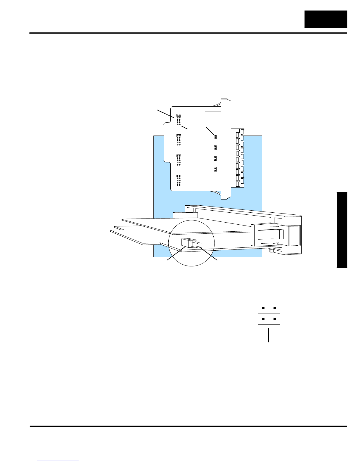
F
3
-
-
0
4
A
D
S
4
-
C
h
.
I
s
olate
dAn
alo
gIn
.
3--
3
Setting the Module Jumpers
Ifyouexaminetherearofthemodule,you’ll
F3--04ADS 4-Channel Isolated Analog Input
Jumper Locations
The module is set at the factory for a 4--20 mA signal on all four channels. If this is
acceptable you do not have to change any of the jumpers. The following diagram
shows how the jumpers are set.
Channel 1
J10
Pin 1
Selecting the
Number of
Channels
UNIPOLAR BIPOLAR
notice several jumpers. The jumpers labeled +1
and +2 (located on the larger board, near the
terminal block) are used to select the number of
channels that will be used.
Without any jumpers the module processes one
channel. By installing the jumpers you can add
channels. The module is set from the factory for
four channel operation.
For example, if you install the +1 jumper, you
add one channel for a total of two. Now if you
install the +2 jumper youadd twomore channels
for a total of four.
Any unused channels are not processed so if
you only select channels 1, 2, and 3, channel 4
will not be active. The table shows which
jumpers to install.
+1
+2
Jumpers installed as shown
selects 4-channel operation
Channel +1 +2
1 No No
1, 2, Yes No
1, 2, 3 No Yes
1, 2, 3, 4 Yes Yes
Page 42
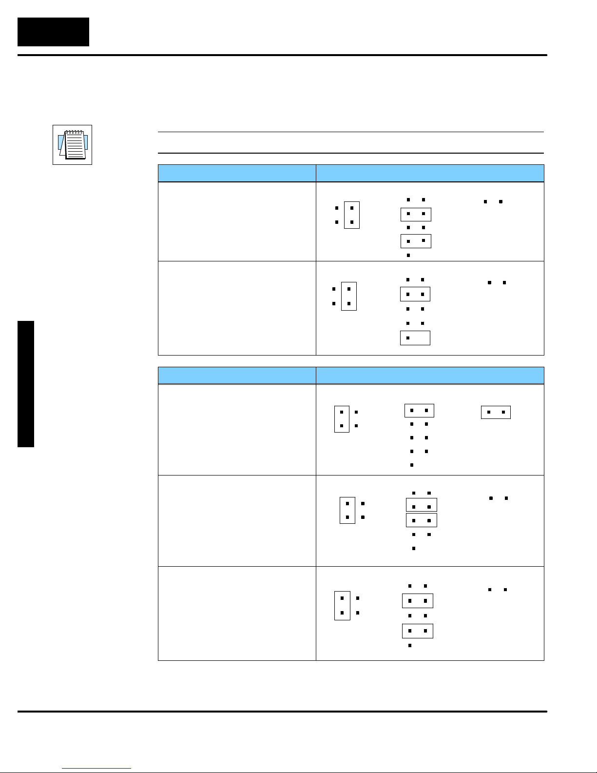
4-Ch.IsolatedAnalogIn
.
3--
4
F3--04ADS 4-Channel Isolated Analog Input
Selecting Input
Signal Ranges
As you examin the jumper settings, notice there are jumpers for each individual
channel. These jumpers allow you to select the type of signal (voltage or current) and
the range of the signal. The following tables show the jumper selections for the
various ranges. Only channel 1 is used in the example, but all channels must be set.
NOTE: The Polarity jumper selects Unipolar or Bipolar operation for all channels.
Bipolar Signal Range Jumper Settings
--5 VDC to +5 VDC
(--20 to +20 mA)
--10 VDC to +10 VDC
Polarity
Uni Bi
Polarity
Uni Bi
Channel 1 Ranges Current Jumper
1
Channel 1 Ranges Current Jumper
1
Unipolar Signal Range Jumper Settings
4 to 20 mA
(1 VDC to 5 VDC, remove the current jumper)
0 VDC to +5 VDC
(0 to +20 mA, install the current
jumper)
0 VDC to +10 VDC
Polarity
Uni Bi
Polarity
Uni Bi
Polarity
Uni Bi
Channel 1 Ranges Current Jumper
1
Channel 1 Ranges Current Jumper
1
Channel 1 Ranges Current Jumper
1
Page 43
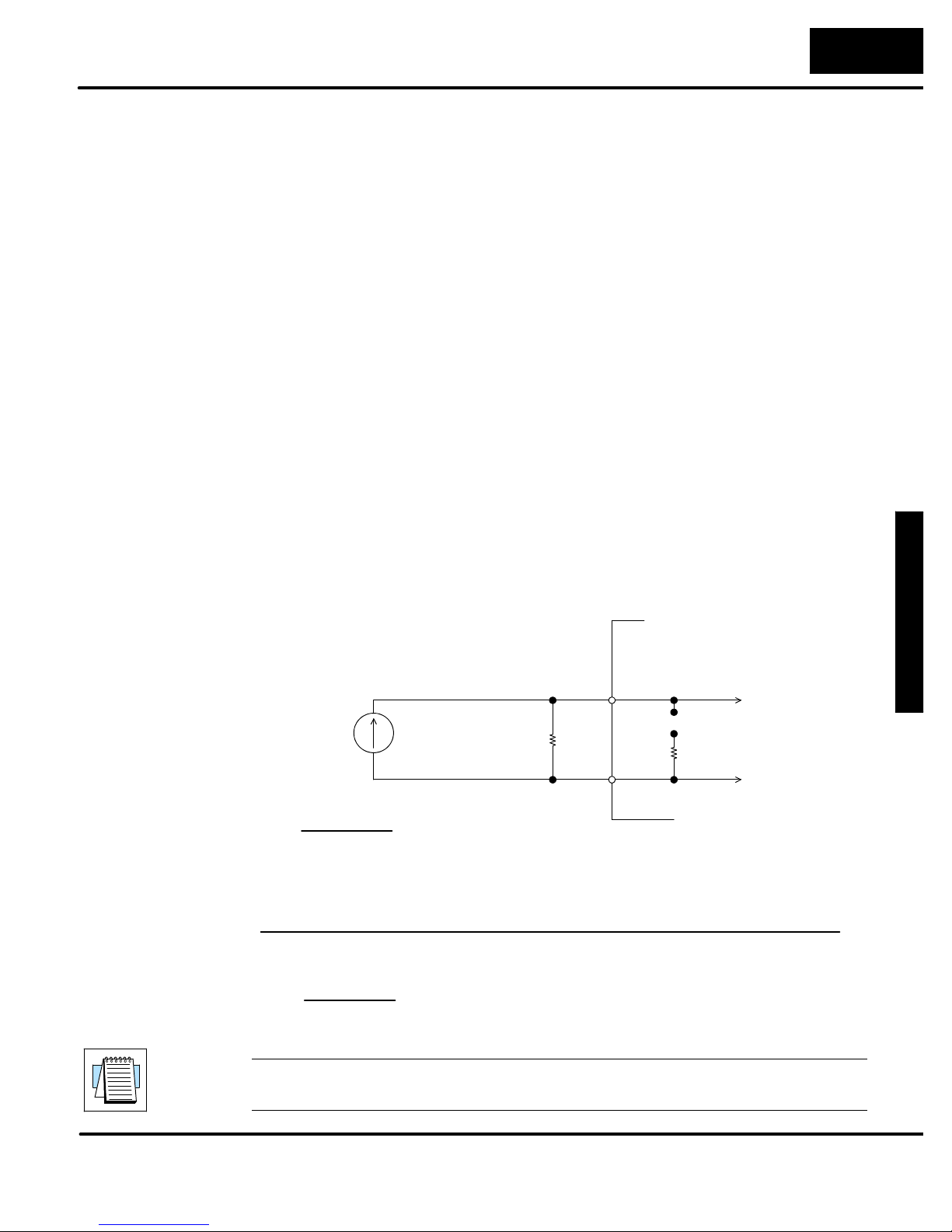
F
3
-
-
0
4
A
D
S
4
-
C
h
.
I
s
olate
dAn
alo
gIn
.
3--
5
Connecting the Field Wiring
F3--04ADS 4-Channel Isolated Analog Input
Wiring Guidelines
User Power Supply
Requirements
Custom Input
Ranges
Your company may have guidelines for wiring and cable installation. If so, you should
check those before you begin the installation. Here are some general things to
consider.
S Use the shortest wiring route whenever possible.
S Use shielded wiring and ground the shield at the signal source. Do not
ground the shield at both the module and the source.
S Do not run the signal wiring next to large motors, high current switches,
or transformers. This may cause noise problems.
S Route the wiring through an approved cable housing to minimize the risk
of accidental damage. Check local and national codes to choose the
correct method for your application.
The F3--04ADS receives all power from the base. A separate power supply is not
required.
Occasionally you may have the need to connect a transmitter with an unusual signal
range. By changing the wiring slightly and adding an external resistor to convert the
current to voltage, you can easily adapt this module to meet the specifications for a
transmitter which does not adhereto one ofthe standard inputranges. The following
diagram shows how this works.
Internal
Module
Circuitry
+
50mA
Current
Transmitter
--
V
R =
R = value of external resistor
V
max
I
max
Example: current transmitter capable of 50mA, 0 -- 10V range selected.
R =
max
I
max
= high limit of selected voltage range
= maximum current supplied by the transmitter
10V
50mA
R = 200 ohms
+CH1
R
-- CH1
Jumper
Removed
250O
+
--
NOTE: Your choice of resistor can affect the accuracy of the module. A resistor with
a ? 0.1% tolerance and a ? 50ppm / _C temperature coefficient is recommended.
Page 44
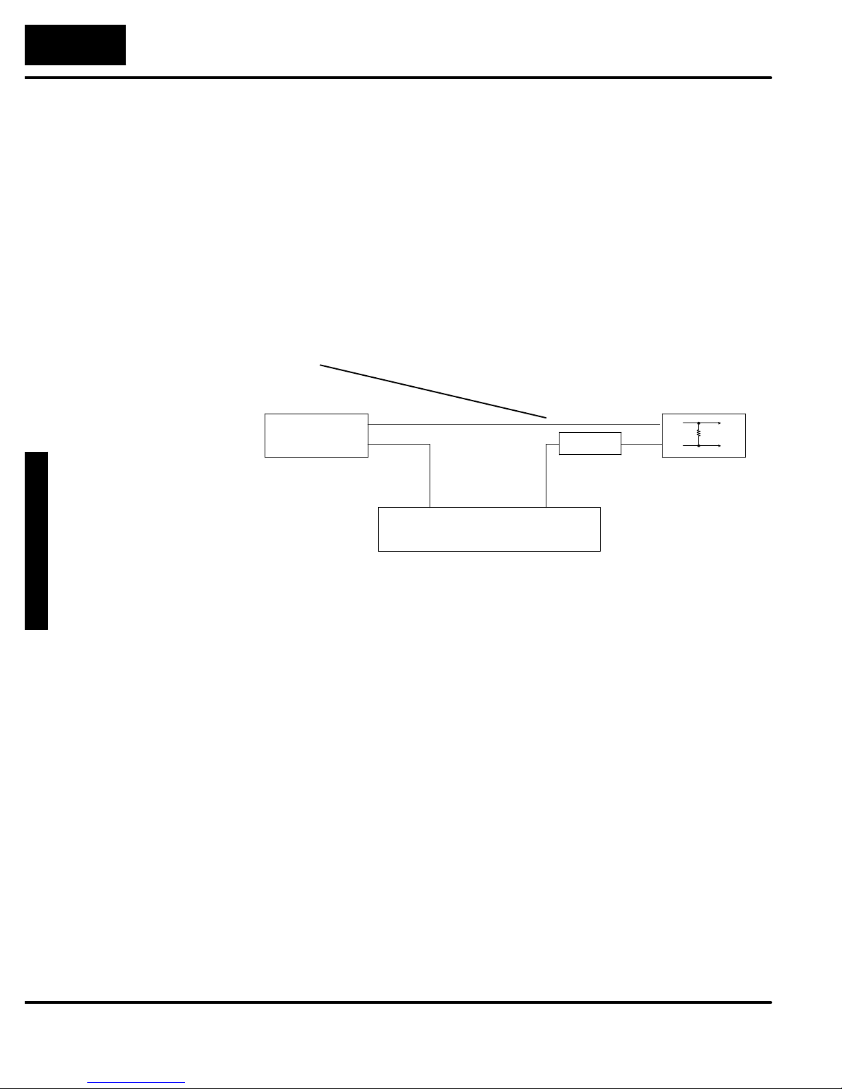
4-Ch.IsolatedAnalogIn
.
3--
6
F3--04ADS 4-Channel Isolated Analog Input
Current Loop
Transmitter
Impedance
Standard 4 to 20 mA transmitters and transducers can operate froma wide variety of
power supplies. Not all transmitters are alike and the manufacturers often specify a
minimum loop or load resistance that must be used with the transmitter.
The F3--04ADS provides 250 ohm resistance for each channel. If your transmitter
requires a load resistance below 250 ohms, then you do not have to make any
adjustments. However, if your transmitter requires a load resistancehigher than 250
ohms, then you need to add a resistor in series with the module.
Consider the following example for a transmitter being operated from a 36 VDC
supply with a recommended load resistance of 750 ohms. Since the module has a
250 ohm resistor, you need to add an additional resistor.
R = Tr - Mr
R = 750 - 250
R = 500
DC Supply
0V
+36V
R -- Resistor to add
Tr -- Transmitter Requirement
Mr -- Module resistance (internal 250 ohms)
Module Channel 1
R
-+
250O
+ --
Two-wire Transmitter
Page 45
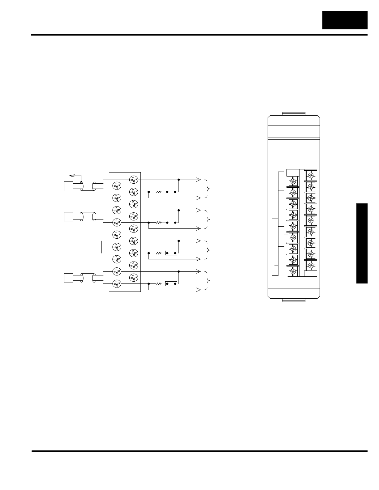
F
3
-
-
0
4
A
D
S
4
-
C
h
.
I
s
olate
dAn
alo
gIn
.
3--
7
F3--04ADS 4-Channel Isolated Analog Input
Removable
Connector
The F3--04ADS module has a removable connector to make wiring easier. Simply
squeeze the top and bottom tabs and gently pull the connector from the module.
Wiring Diagram
Note 1: Connect unused voltage or current inputs to 0VDC
at terminal block or leave current jumper installed
(see Channel 3).
Note 2: A Series 217, 0.032A, Fast-acting fuse is
recommended for 4-- 20mA current loops.
Note 3: Transmitters may be 2, 3, or 4 wire type.
Note 4: Transmitters may be powered from separate
power sources.
Note 5: Terminate all shields of the cable at their respective
signal source.
See Notes
CH1
+
Voltage
Transmitter
CH2
Voltage
Transmitter
CH4
4--20mA
Current
Transmitter
--
+
--
CH3
Not Used
+
--
250
250 J11
250 J13
CH3
250 J14
Installed
CH4 Jumper
Internal Module Wiring
+
J10
--
+
--
+
Jumper
Installed
--
+
--
to
Analog
Circuitry
to
Analog
Circuitry
to
Analog
Circuitry
to
Analog
Circuitry
ANALOG INPUT
F3-- 04ADS
+
1
--
+
2
--
+
3
--
+
4
--
Page 46
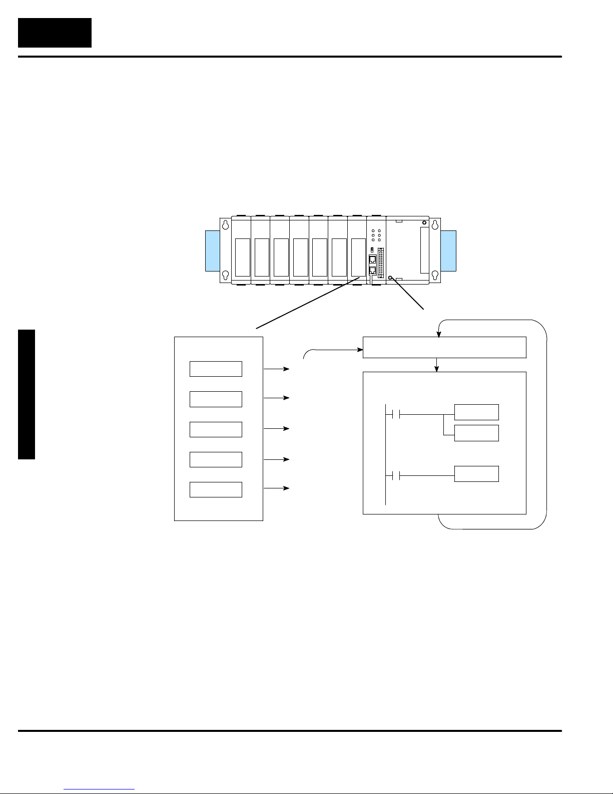
4-Ch.IsolatedAnalogIn
.
3--
8
F3--04ADS 4-Channel Isolated Analog Input
Module Operation
Before you begin writing the control program, it is important to take a few minutes to
understand how the module processes and represents the analog signals.
Channel Scanning
Sequence
The F3--04ADS module supplies1 channel of data per each CPU scan. Since there
are four channels, it can take up to four scans to get data for all channels. Once all
channels have been scanned the process starts over with channel 1.
You do not have to select all of the channels. Unused channels are not processed, so
if you select only two channels, then each channel will be updated every other scan.
Scan
I/O Update
Channel 1
Scan N
Execute Application Program
Channel 2
Channel 3
Channel 4
Channel 1
Scan N+1
Scan N+2
Scan N+3
Scan N+4
Read the data
Store data
Even though the channel updates to the CPU are synchronous with the CPU scan,
the module asynchronously monitors the analog transmitter signal and converts the
signal to a 12-bit binary representation. This enables the module to continuously
provide accurate measurements without slowing down the discrete control logic in
the RLL program.
Page 47
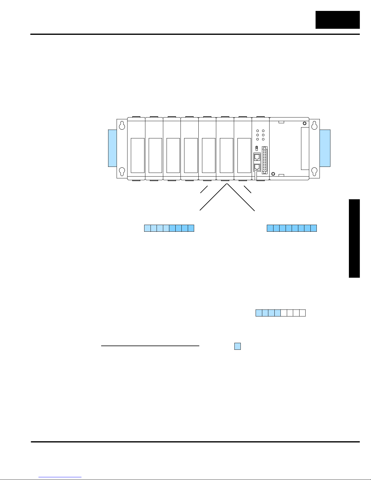
F
3
-
-
0
4
A
D
S
4
-
C
h
.
I
s
olate
dAn
alo
gIn
.
3--
9
F3--04ADS 4-Channel Isolated Analog Input
F3--04ADS
Understanding the
I/O Assignments
You may recall the F3--04ADS module appears to the CPU as a 16-point module.
These 16 points provide:
S an indication of which channel is active.
S the digital representation of the analog signal.
Since all I/O points are automatically mapped into Register (R) memory, it is very
easy to determine the location of the data word that will be assigned to the module.
8pt
Relay
050
057
8pt
Output
--
Output
040
--
047
R 002, R012 R 000, R010
R 011
MSB LSB
8pt
030
--
037
16pt
Input
020
027
-120
127
4ch.
(Analog)
010
017
-110
117
16pt
Input
000
007
100
107
--
R 001
MSB LSB
Active Channel
Selection Inputs
1
1
7
1
1
0
0
1
7
0
1
0
Within these two register locations, the individual bits represent specific information
about the analog signal.
The last four points of the upper register
are used as inputs to tell the CPU which
channel is being processed. In our
MSB LSB
R011
example, when input 114 is on the
module is telling the CPU it is processing
channel 1. Here’s how the inputs are
assigned.
Input Active Channel
1
1
1
1
1
1
1
1
1
1
7
6
5
4
3
-- channel selection inputs
1
1
1
1
1
1
0
2
1
114 1
115 2
116 3
117 4
Page 48
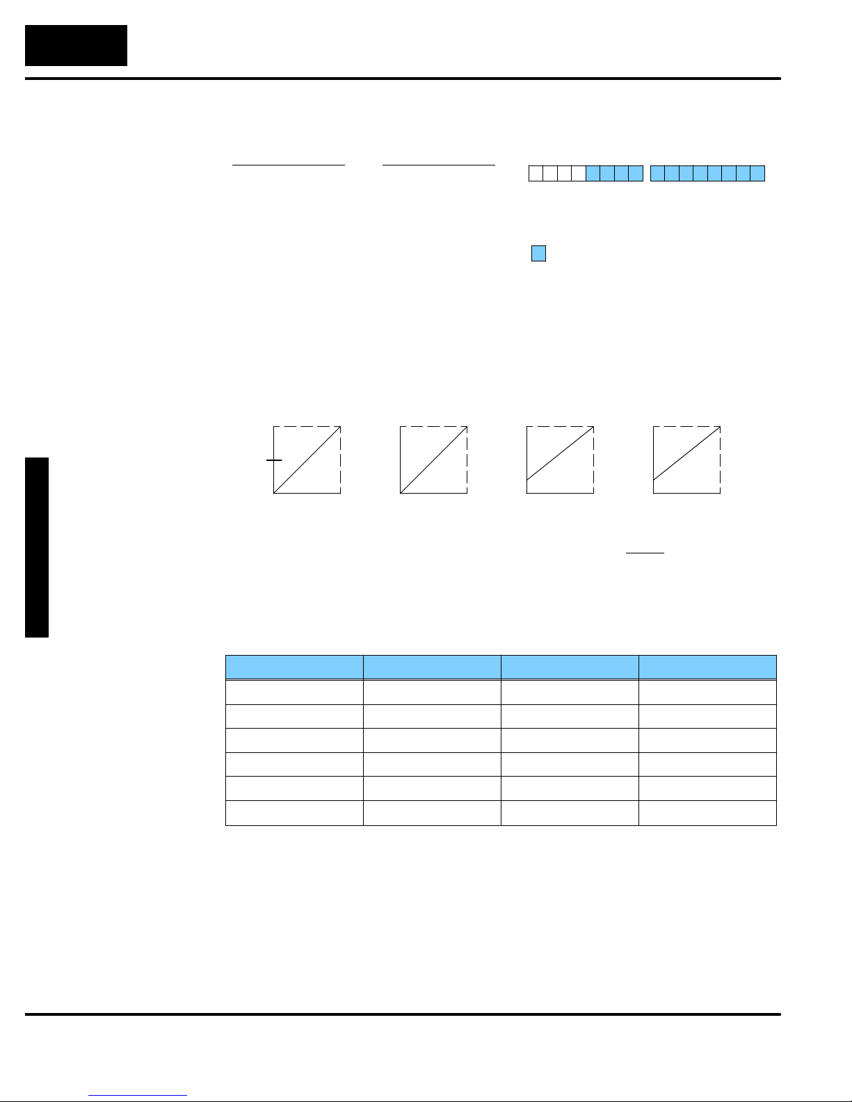
4-Ch.IsolatedAnalogIn
.
3--10
F3--04ADS 4-Channel Isolated Analog Input
Theremainingtwelvebitsrepresentth
e
Analog Data Bits
analog data in binary format.
Bit Value Bit Value
0 (LSB) 1 6 64
1 2 7 128
2 4 8 256
3 8 9 512
4 16 10 1024
R011
MSB LSB
1
1
1
1
1
1
1
1
1
1
1
1
1
1
1
1
7
6
5
4
3
2
1
0
-- data bits
R001
0
0
0
0
0
1
1
1
1
1
7
6
5
4
3
0
0
0
1
1
1
0
2
1
5 32 11 2048
Since the module has 12-bit resolution, the analog signal is converted into 4096
“pieces” ranging from 0 -- 4095 (212). For example, with a 0 to 10V scale, a 0V signal
would be 0, and a 10V signal would be 4095. This is equivalent to a a binary value of
0000 0000 0000 to 1111 1111 1111, or 000 to FFF hexadecimal. The following
diagram shows how this relates to each signal range.
--10V -- +10V
--5V -- +5V
+V
0V
-- V
0 4095
Each “piece” can also be expressed in
terms of the signal level by using the
0V -- 10V
0V -- 5V
+V
0V
0 4095
+5V
1V
0 4095
1V -- 5V
Resolution =
4 -- 20mA
20mA
4mA
0 4095
H - L
4095
equation shown. The following table
shows the smallest signal levels that will
result in a change in the data value for
each signal range.
H = high limit of the signal range
L = low limit of the signal range
Range Highest Signal Lowest Signal Smallest Change
--10 to +10V +10V --10V 4.88 mV
--5 to +5V +5 V --5V 2.44 mV
0 to 5V 5V 0V 1.22 mV
0 to 10V 10 V 0V 2.44 mV
1 to 5V 5V 1V 0.98 mV
4 to 20mA 20mA 4mA
Now that you understand how the module and CPU work together to gather and
store the information, you’re ready to write the control program.
3.91 µA
Page 49
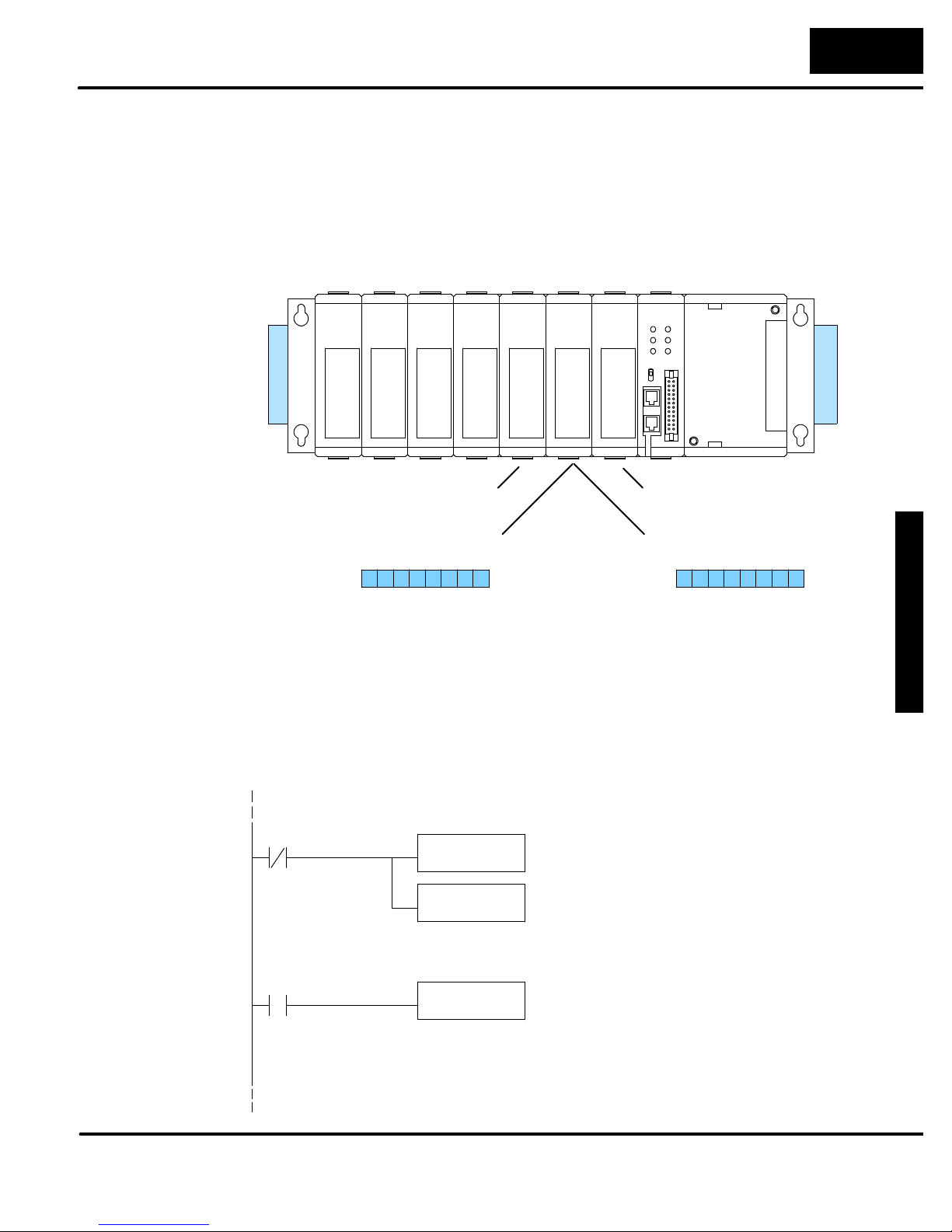
F
3
-
-
0
4
A
D
S
4
-
C
h
.
I
s
olate
dAn
alo
gIn
.
3--11
Writing the Control Program
F3--04ADS
F3--04ADS 4-Channel Isolated Analog Input
Identifying the
Data Locations
Since all channels are multiplexed into a single data word, the control program must
be setup to determine which channel is being read. Since the module provides input
points to the CPU, it is very easy to use the active channel status bits to determine
which channel is being monitored.
8pt
Relay
050
057
8pt
Output
Output
040
--
--
047
R 002, R012 R 000, R010
R 011
MSB LSB
1
1
7
8pt
030
--
037
16pt
Input
020
027
120
127
(Analog)
--
4ch.
010
017
-110
117
16pt
Input
000
007
100
107
--
R 001
MSB LSB
1
1
0
0
1
7
0
1
0
Single Channel on
Every Scan
The following example shows a program that is designed to read a single channel of
analog data into a Register location on every scan. Once the data is in a Register,
you can perform math on the data, comparethe data againstpreset values, etc. This
example is designed to read channel 1. Since you use jumpers to select the number
of channels to scan, this is the only channel that you can use in this manner.
Read the data
374
Store channel 1
114
DSTR1
R001
BCD F86
DOUT
R400
F51
F60
This rung loads the data into the accumulator on
every scan. (You can use any permissive contact.)
The DL305 CPUs perform math operations in
BCD. This instruction converts the binary data to
BCD. (You can omit this step if your application
does not require the conversion.)
The active channel inputs are used to let the CPU
know which channel has been loaded into the
accumulator. (Since you cannot isolate the
individual channels for scanning, channel 1 is the
only channel that can be used in this manner.) By
using the input to control a DOUT instruction, you
can easily move the data to a storage register. The
BCD value will be stored in R400 and R401. (Two
bytes are required for four digit BCD numbers.)
Page 50
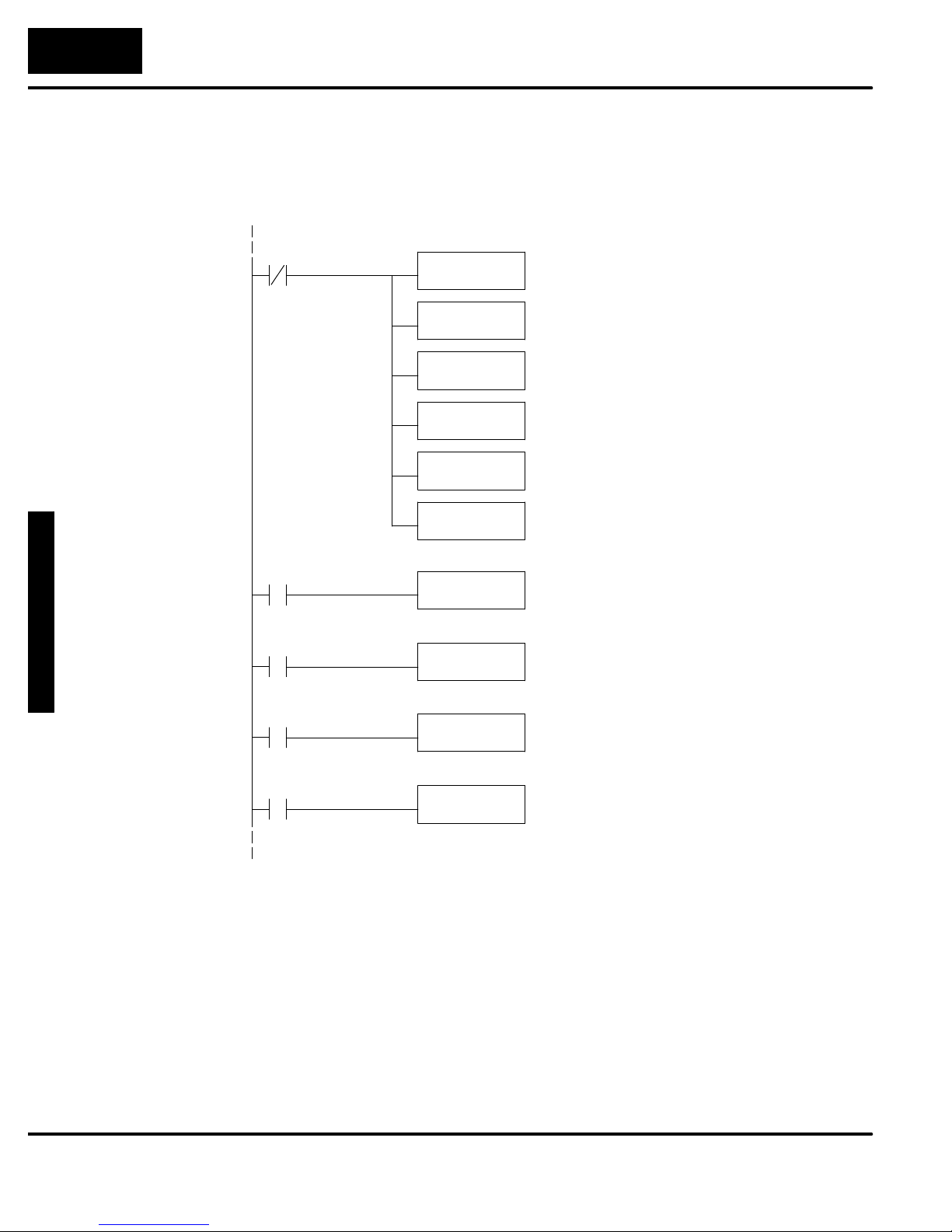
4-Ch.IsolatedAnalogIn
.
3--12
F3--04ADS 4-Channel Isolated Analog Input
Reading Multiple
Channels over
Alternating Scans
The following example shows a program designed to read any of the available
channels of analog data into Register locations. Once the data is in a Register, you
can perform math on the data, compare the data against preset values, etc. Since
the DL305 CPUs use 8-bit word instructions, you have to move the data in pieces. It’s
simple if you follow the example.
Read the data
374
Store channel 1
114
Store channel 2
115
DSTR3
R011
DOUT1
R501
DSTR1
R001
DOUT1
R500
DSTR
R500
BCD F86
DOUT
R400
DOUT
R402
F53
F61
F51
F61
F50
F60
F60
This rung loads the four most significant data bits
into the accumulator from Register 011. (A normally
closed 374 means it is loaded on every scan.)
Temporarily store the bits to Register 501.
This rung loads the eight least significant data bits
into the accumulator from Register 001.
Temporarily store the bits to Register 500. Since
the most significant bits were loaded into 501, now
R500 and R501 contain all twelve bits in order.
Now that all the bits are stored, load all twelve bits
into the accumulator.
Math operations are performed in BCD. This
instruction converts the binary data to BCD. (You
can omit this step if your application does not
require the conversion.)
The channel selection inputs are used to let the
CPU know which channel has been loaded into the
accumulator. By using these inputs to control a
DOUT instruction, you can easily move the data to
a storage register. Notice the DOUT instruction
stores the data in two bytes. (Two bytes are
required for four digit BCD numbers.)
Store channel 3
116
Store channel 4
117
DOUT
R404
DOUT
R406
F60
F60
Page 51
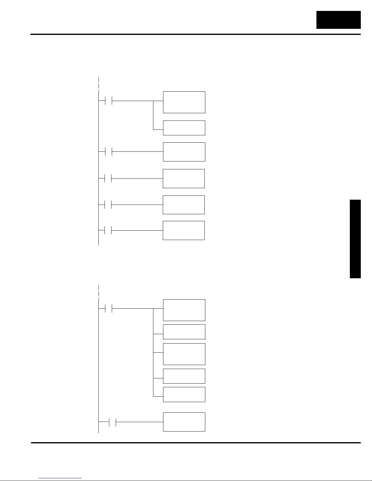
F
3
-
-
0
4
A
D
S
4
-
C
h
.
I
s
olate
dAn
alo
gIn
.
3--13
F3--04ADS 4-Channel Isolated Analog Input
Reading Multiple
Channels over
Alternating Scans
on a DL350 with a
D3--XX--1 Base
The example below shows how to scale input data from an F3--04ADS Analog
module in the X0 position of the D3--XX--1 base. This module must be placed in a 16
bit slot in order to work.
Load the data
_On
SP1
Channel 1 Select Bit
X14
Channel 2 Select Bit
X15
Channel 3 Select Bit
X16
Channel 4 Select Bit
X17
LDF
BCD
OUT
OUT
V2001
OUT
V2002
OUT
V2003
V2000
X0
K12
This rung loads the first twelve bits of data from X0
and then converts it to BCD format.
This writes channel one analog data to V2000
when X14 (channel select 1) is on.
This writes channel two analog data to V2001
when X15 (channel select 2) is on.
This writes channel three analog data to V2002
when X16 (channel select 3) is on.
This writes channel four analog data to V2003
when X17 (channel select 4) is on.
Reading Multiple
Channels over
Alternating Scans
on a DL350 with a
Conventional Base
The example below shows how to read multiple channels on an F3--04ADS Analog
module in the 20--27/120--127 address slot. This module must be placed in a 16 bit
slot in order to work.
Load the data
_On
SP1
Channel 1 Select Bit
X124
LDFK8X120
SHFL
ORFK8X20
ANDD
BCD
OUT
K8
Kfff
V3000
This rung loads the upper byte of analog data from
the module.
SHFL K8 shifts the data to the left eight places to
make room for the lower byte of data.
The ORF X20 brings the lower byte of data from
the module into the accumulator. At this time there
is a full word of data from the analog module in the
accumulator.
The ANDD Kfff masks off the twelve least
significant bits of data from the word. This is the
actual analog value.
The BCD command converts the data to BCD
format.
This writes channel one analog data to V3000
when the Channel 1 Select Bit (X124) is set.
Page 52

4-Ch.IsolatedAnalogIn
.
3--14
F3--04ADS 4-Channel Isolated Analog Input
Thefollowingexampleshowshowyo
u
Scaling the Input
Data
Most applications usually require
measurements in engineering units,
which provide more meaningful data.
This is accomplished by using the
conversion formula shown.
would use the analog data to represent
pressure (PSI) from 0 to 100. This
example assumes the analog value is
1760. This should yield approximately
42.9 PSI.
Units =
Units = value in Engineering Units
A = Analog value (0 -- 4095)
S = high limit of the Engineering
unit range
A
S
4096
Units =
Units =
Units = 42.9
4096
1760
4096
A
S
100
Page 53

F
3
-
-
0
4
A
D
S
4
-
C
h
.
I
s
olate
dAn
alo
gIn
.
3--15
F3--04ADS 4-Channel Isolated Analog Input
The following instructions are required to scale the data. We’ll continue to use the
42.9 PSI example. In this example we’re using channel 1. Input 114 is the active
channel indicator for channel 1. Of course, if you were using a different channel, you
would use the active channel indicator point that corresponds to the channel you
were using.
This example assumes you have already read the analog data
and stored the BCD equivalent in R400 and R401
Scale the data
114
DSTR
R400
F50
This instruction brings the analog value (in BCD)
into the accumulator.
Accumulator
1 7 6 0
Aux. Accumulator
0 0 0 0
R577 R576
DIV
K4096
DSTR
R576
MUL
K100
DSTR
R576
DOUT
R450
F74
F50
F73
F50
F60
The analog value is divided by the resolution of the
module, which is 4096. (1760 / 4096 = 0.4296)
Accumulator
0 0 0 0
This instruction moves the two-byte decimal
portion into the accumulator for further operations.
Accumulator
4 2 9 6
The accumulator is then multiplied by the scaling
factor, which is 100. (100 x 4296 = 429600). Notice
the most significant digits are now stored in the
auxilliary accumulator. (This is different from the
way the Divide instruction operates.)
Accumulator
9 6 0 0
This instruction moves the two-byte auxilliary
accumulator for further operations.
Accumulator
0 0 4 2
Aux. Accumulator
4 2 9 6
R577 R576
Aux. Accumulator
4 2 9 6
R577 R576
Aux. Accumulator
0 0 4 2
R577 R576
Aux. Accumulator
0 0 4 2
R577 R576
This instruction stores the accumulator to R450.
R450 now contains the PSI, which is 42 PSI.
Accumulator
0 0 4 2
Store in R451 & R450
0 0 4 2
R451 R450
Page 54
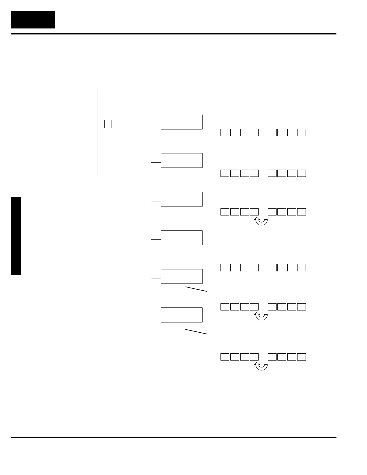
4-Ch.IsolatedAnalogIn
.
3--16
F3--04ADS 4-Channel Isolated Analog Input
You probably noticed the previous example yielded 42 PSI when the real value
should have been 42.9 PSI. By changingthe scalingvalue slightly, we can “imply” an
extra decimal of precision. Notice in the following example we’ve added another digit
to the scale. Instead of a scale of 100, we’re using 1000, which implies 100.0 for the
PSI range.
This example assumes you have already read the analog data
and stored the BCD equivalent in R400 and R401
Scale the data
114
DSTR
R400
F50
This instruction brings the analog value (in BCD)
into the accumulator.
Accumulator
1 7 6 0
Aux. Accumulator
0 0 0 0
R577 R576
DIV
K4096
DSTR
R576
MUL
K1000
DSTR
R576
DOUT
R450
F74
F50
F73
F50
F60
The analog value is divided by the resolution of the
module, which is 4096. (1760 / 4096 = 0.4296)
Accumulator
0 0 0 0
This instruction moves the two-byte decimal
portion into the accumulator for further operations.
Accumulator
4 2 9 6
The accumulator is multiplied by the scaling factor,
which is now 1000. (1000 x 4296 = 4296000). The
most significant digits are now stored in the
auxilliary accumulator. (This is different from the
way the Divide instruction operates.)
Accumulator
6 0 0 0
This instruction moves the two-byte auxilliary
accumulator for further operations.
Accumulator
0 4 2 9
Aux. Accumulator
4 2 9 6
R577 R576
Aux. Accumulator
4 2 9 6
R577 R576
Aux. Accumulator
0 4 2 9
R577 R576
Aux. Accumulator
0 4 2 9
R577 R576
This instruction stores the accumulator to R450
and R451. R450 and R451 now contain the PSI,
which implies 42.9.
Accumulator
0 4 2 9
Store in R451 & R450
0 4 2 9
R451 R450
Page 55
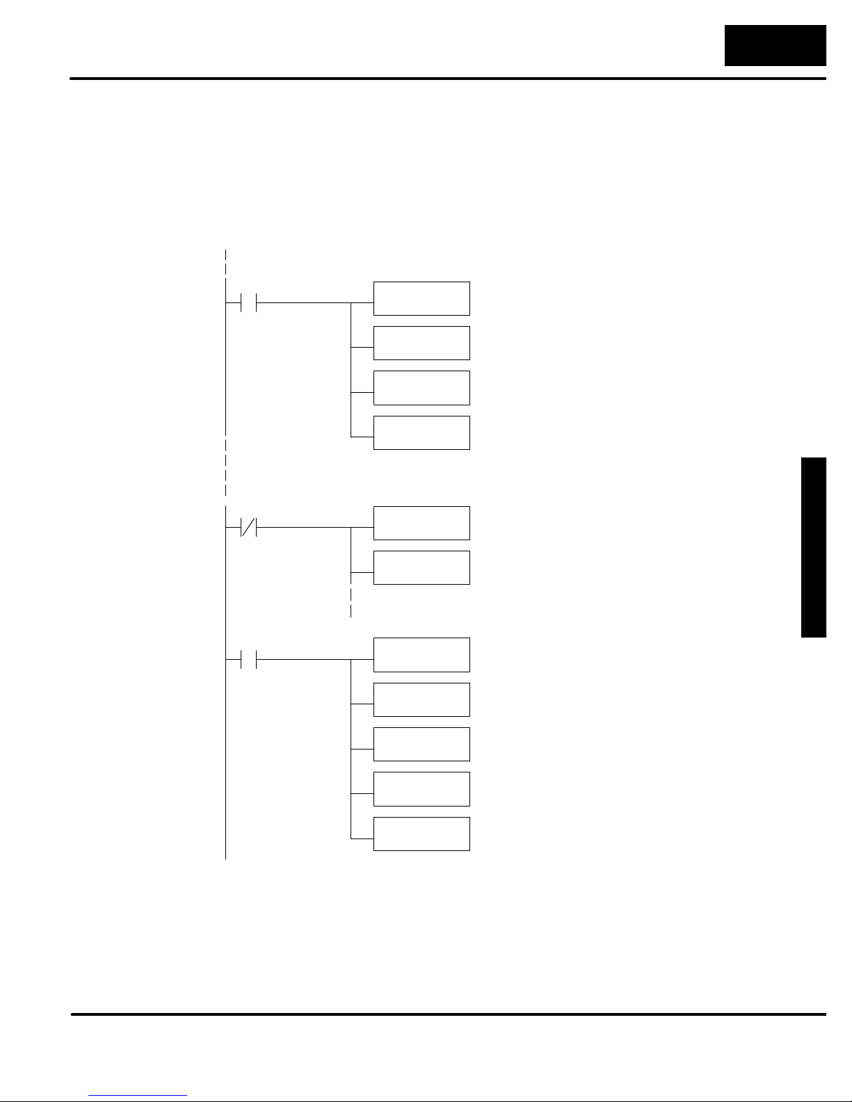
F
3
-
-
0
4
A
D
S
4
-
C
h
.
I
s
olate
dAn
alo
gIn
.
3--17
F3--04ADS 4-Channel Isolated Analog Input
This example program shows how you can use the instructions to load these
equation constants into data registers. The example is written for channel 1, but you
can easily use a similar approach to use different scales for all channels if required.
You may just use the appropriate constants in the instructions dedicated for each
channel, but this method allows easier modifications. For example, you could easily
use an operator interface or a programming device to change the constants if they
are stored in Registers.
Load the constants
374
DSTR
K4096
F50
On the first scan, these first two instructions load
the analog resolution (constant of 4096) into R430
and R431.
Read the data
374
Store channel 1
114
DOUT
R430
DSTR
K1000
DOUT
R432
DSTR3
R011
DOUT1
R501
DIV
R430
DSTR
R576
MUL
R432
F60
F50
F60
F53
F61
F74
F50
F73
These two instructions load the high limit of the
Engineering unit scale (constant of 1000) into
R432 and R433. Note, if you have different scales
for each channel, you’ll also have to enter the
Engineering unit high limit for those as well.
This rung loads the four most significant data bits
into the accumulator from Register 011.
Temporarily store the bits to Register 501.
The analog value is divided by the resolution of the
module, which is stored in R430.
This instruction moves the decimal portion from the
auxilliary accumulator into the regular accumulator
for further operations.
The accumulator is multiplied by the scaling factor,
which is stored in R432.
DSTR
R576
DOUT
R400
F50
F60
This instruction moves most significant digits (now
stored in the auxilliary accumulator) into the
regular accumulator for further operations.
The scaled value is stored in R400 and R401 for
further use.
Page 56
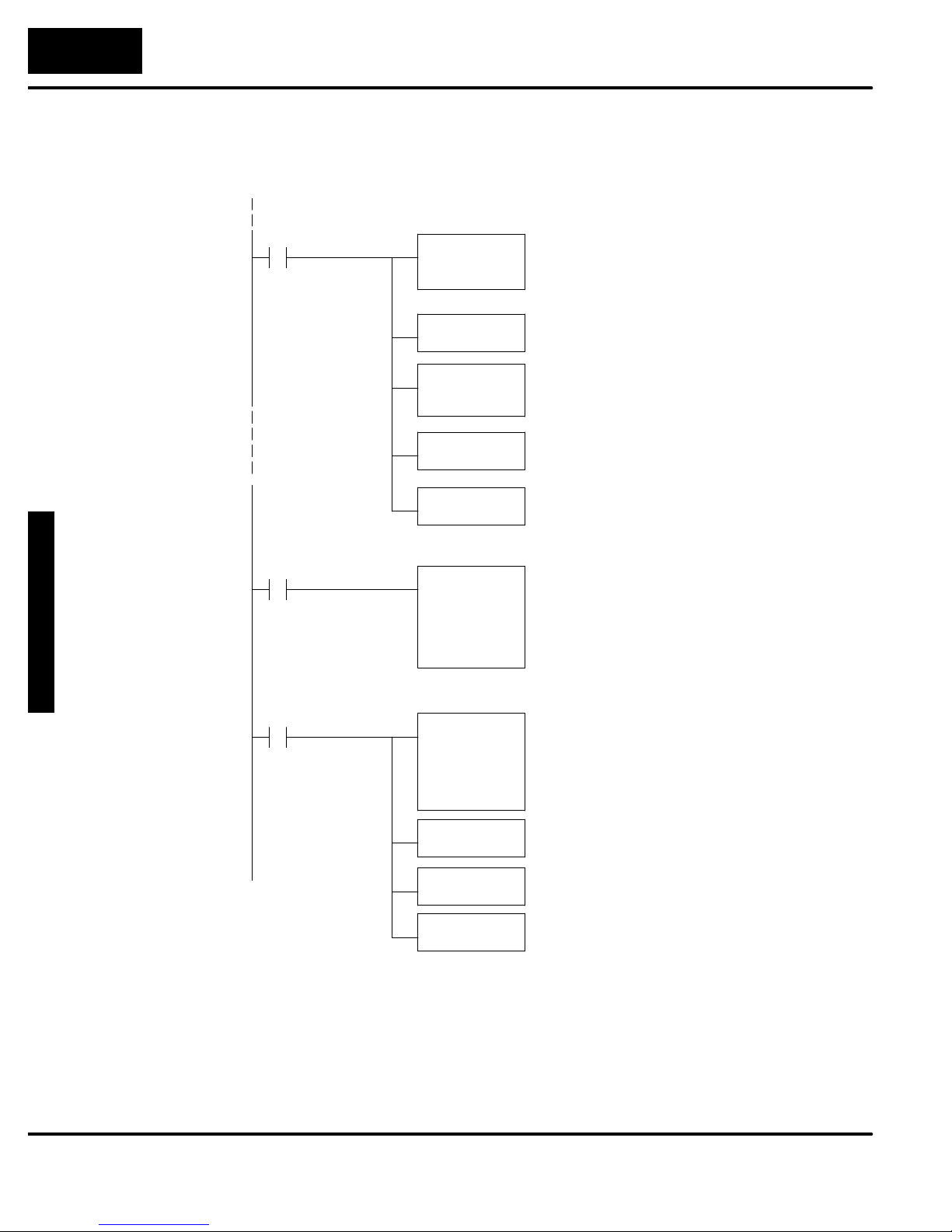
4-Ch.IsolatedAnalogIn
.
3--18
F3--04ADS 4-Channel Isolated Analog Input
Scaling on a DL350
with a
Conventional
DL305 Base
The example below shows how to scale input data from an F3--04ADS Analog
module in the 20--27/120--127 address slot. This module must be placed in a 16 bit
slot in order to work.
Load the data
_On
SP1
Select Channel 2
Channel 2 Select Bit
X125
Scale the data
_On
SP1
LDFK8X120
SHFL K8
ORF
ANDD Kfff
BCD
OUT
Channel 2
Analog Data
Register (BCD)
LD
Channel 2
Analog Data
Register (BCD)
X20
K8
V3001
V3001
This loads the upper byte of the analog data from
the module.
SHFL K8 shifts the data to the left eight places to
make room for the lower byte of data.
The ORF X20 brings the lower byte of data from
the module into the accumulator. At this time there
is a full word of data from the analog module in the
accumulator.
The ANDD Kfff masks off the twelve least
significant bits of data from the word. This is the
actual analog value.
The BCD command converts the data to BCD
format.
X125 is the channel select bit for channel two. This
rung puts the data from the analog module into the
respective V--memory location.
Rung 3 scales a 0 to 180 range of a transducer
over the 4096 counts. The raw analog value is
loaded to the accumulator from V3001
(Channel #2).
MUL K1800
DIV K4096
OUT V3010
It is then multiplied by 1800. The additional zero
provides a higher degree of resolution.
It is then divided by 4096, which is the resolution of
the module.
The scaled value is stored in V3010 with an
implied decimal.
Page 57
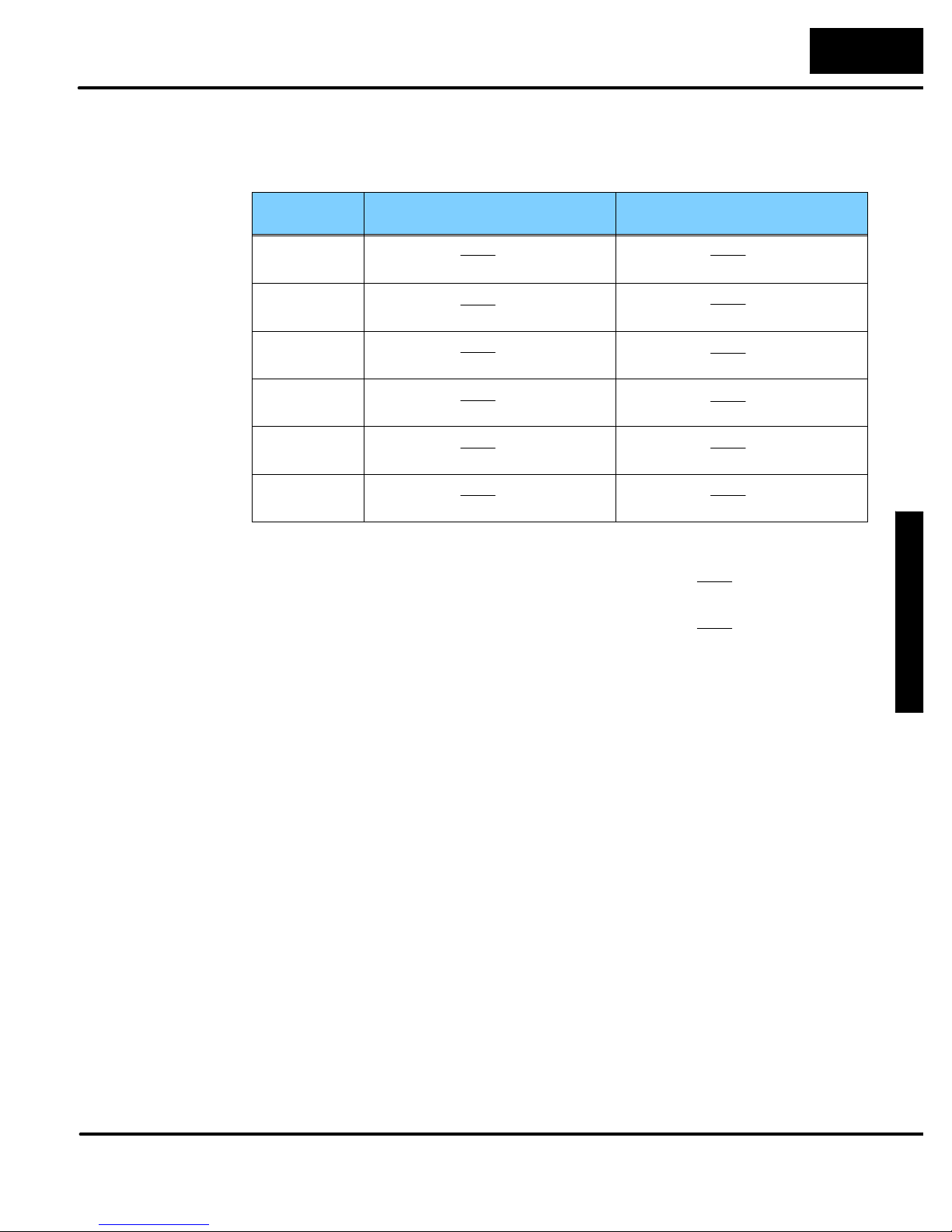
F
3
-
-
0
4
A
D
S
4
-
C
h
.
I
s
olate
dAn
alo
gIn
.
3--19
F3--04ADS 4-Channel Isolated Analog Input
Analog and Digital
Value Conversions
Sometimes it is helpful to be able to quickly convert between the signal levels and the
digital values. This is especially helpful during machine startup or troubleshooting.
The following table provides formulas to make this conversion easier.
Range If you know the digital value ... If you know the analog signal
level ...
--10V to + 10V
--5V to + 5V
0 to 5V
0 to 10V
1 to 5V
4 to 20mA
A =
A =
A =
A =
A =
A =
20D
- 10
4095
10D
- 5
4095
5D
4095
10D
4095
4D
+ 1 D =
4095
16D
+ 4
4095
For example, if you are using the --10 to
+10V range and you have measured the
D =
D =
D =
D =
D =
D =
4095
4095
4095
4095
4095
4095
4095
20
(A + 10)
20
(A + 5)
10
A
5
A
10
(A - 1)
4
(A - 4)
16
(A + 10)
signal at 6V, you would use the following
formula to determine the digital value
that should be stored in the register
location that contains the data.
4095
D =
D = (204.75) (16)
(6V + 10)
20
D = 3276
Now you have all the necessary information to get your analog module installed and
operating correctly!
Page 58

1
4
F3--08AD
8-Channel
Analog Input
In This Chapter. . . .
— Module Specifications
— Setting the Module Jumpers
— Connecting the Field Wiring
— Module Operation
— Writing the Control Program
Page 59

8-ChannelAnalogInpu
t
4--
2
F3--08AD 8-Channel Analog Input
Module Specifications
The following table provides the specifications for the F3--08AD Analog Input
Module from FACTS Engineering. Review these specifications to make sure the
module meets your application requirements.
Number of Channels 8, single ended (one common)
Input Ranges 4 -- 20 mA
Resolution 12 bit (1 in 4096)
Input Impedance 250O ? 0.1%, 1/2W current input
Absolute Maximum Ratings ? 30mA
Analog Input
Configuration
Requirements
Conversion Time
Converter Type Successive Approximation, AD574
Linearity Error ? 1 count (0.03% of full scale) maximum
Maximum Inaccuracy 0.35% of full scale at 77 °F (25 °C)
Accuracy vs. Temperature
Recommended Fuse 0.032 A, Series 217 fast-acting
Power Budget Requirement 25 mA @ 9 VDC, 37 mA @ 24 VDC
External Power Supply None required
Operating Temperature
Storage Temperature
Relative Humidity 5 to 95% (non-condensing)
Environmental air No corrosive gases permitted
Vibration MIL STD 810C 514.2
Shock MIL STD 810C 516.2
Noise Immunity NEMA ICS3--304
The F3--08AD Analog Input appears as a 16-point module. The module can be
installed in any slot configured for 16 points. See the DL305 User Manual for details
on using 16 point modules in DL305 systems. The limitation onthe number ofanalog
modules are:
S For local and expansion systems, the available power budget and
16-point module usage are the limiting factors.
35µs per channel
1 channel per CPU scan
57 ppm / _C maximum full scale (including
maximum offset change of 2 counts)
32° to 140° F (0° to 60_ C)
--4° to 158° F (--20° to 70_ C)
Page 60
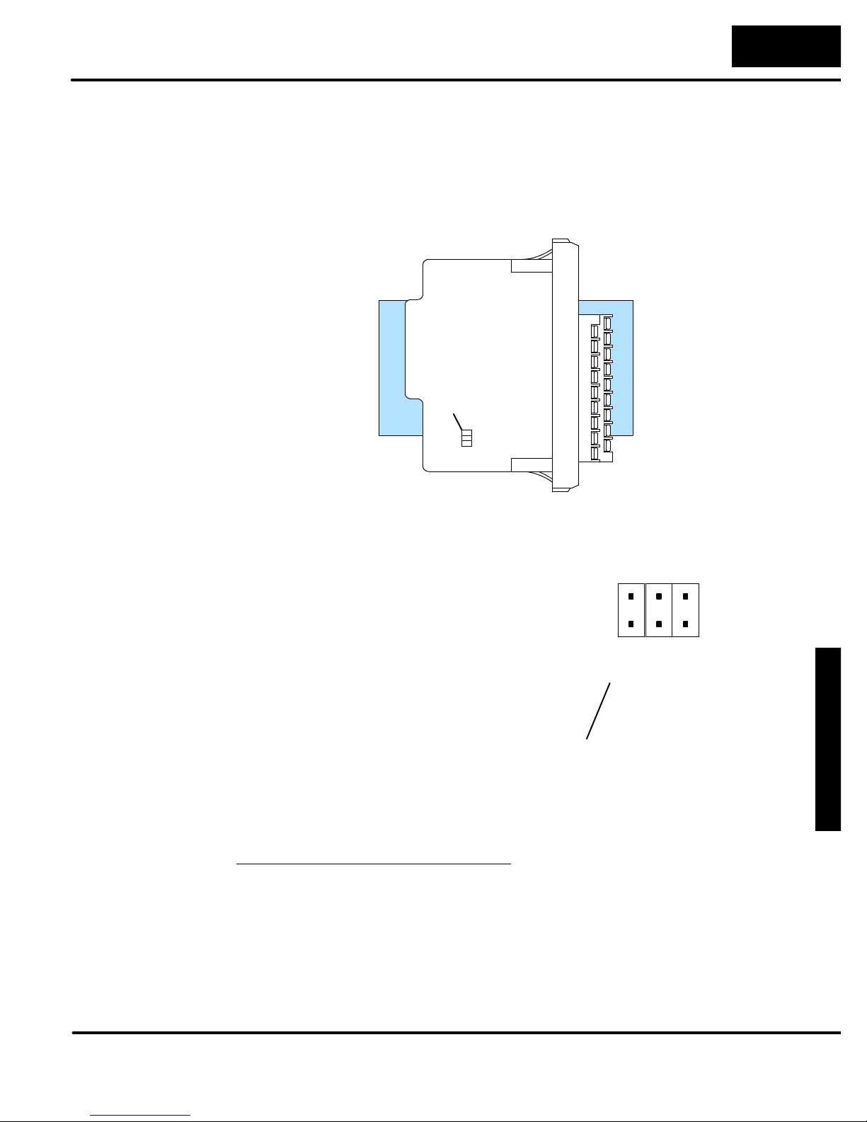
F
3
-
-
0
8
A
D
8
-
C
hanne
l
A
n
alo
gInpu
t
4--
3
Setting the Module Jumpers
Ifyouexaminetherearofthemodule,
12345678YesYesYes
F3--08AD 8-Channel Analog Input
Jumper Locations
Selecting the
Number of
Channels
The module is set at the factory for a 4--20 mA signal on all eight channels. If this is
acceptable you do not have to change any of the jumpers. The following diagram
shows how the jumpers are set.
Channels
+4
+2
+1
you’ll notice several jumpers. The
jumpers labeled +1, +2 and +4 are used
to select the number of channels that will
be used. Without any jumpers the
module processes one channel (channel
1). By installing the jumpers you can add
channels. The module is set from the
factory for eight channel operation.
For example, if you install the +1 jumper,
you add one channel for a total of two.
Now if you install the +2 jumper you add
two more channels for a total of four.
Any unused channels are not processed
so if you only select channels 1--4, then
the last four channels will not be active.
The following table shows which jumpers
to install.
Channel(s) +4 +2 +1
1 No No No
1 2 No No Yes
1 2 3 No Yes No
1 2 3 4 No Yes Yes
1 2 3 4 5 Yes No No
1 2 3 4 5 6 Yes No Yes
1 2 3 4 5 6 7 Yes Yes No
Jumpers installed as shown
selects 8-channel operation
+4 +2 +1
Number of
Channels
Page 61

8-ChannelAnalogInpu
t
4--
4
F3--08AD 8-Channel Analog Input
Connecting the Field Wiring
Wiring Guidelines
User Power Supply
Requirements
Current Loop
Transmitter
Impedance
Your company may have guidelines for wiring and cable installation. If so, you should
check those before you begin the installation. Here are some general things to
consider.
S Use the shortest wiring route whenever possible.
S Use shielded wiring and ground the shield at the signal source. Do not
ground the shield at both the module and the source.
S Don’t run the signal wiring next to large motors, high current switches, or
transformers. This may cause noise problems.
S Route the wiring through an approved cable housing to minimize the risk
of accidental damage. Check local and national codes to choose the
correct method for your application.
The F3--08AD receives all power from the base. A separate power supply is not
required.
Standard 4 to 20 mA transmitters and transducers can operate froma wide variety of
power supplies. Not all transmitters are alike and the manufacturers often specify a
minimum loop or load resistance that must be used with the transmitter.
The F3--08AD provides 250 ohm resistance for each channel. If your transmitter
requires a load resistance below 250 ohms, then you do not have to make any
adjustments. However, if your transmitter requires a load resistancehigher than 250
ohms, then you need to add a resistor in series with the module.
Consider the following example for a transmitter being operated from a 36 VDC
supply with a recommended load resistance of 750 ohms. Since the module has a
250 ohm resistor, you need to add an additional resistor.
R = Tr - Mr
R = 750 - 250
R = 500
DC Supply
+36V
0V
R -- Resistor to add
Tr -- Transmitter Requirement
Mr -- Module resistance (internal 250 ohms)
Module Channel 1
R
+ --
Two-wire Transmitter
--
+
250O
Page 62
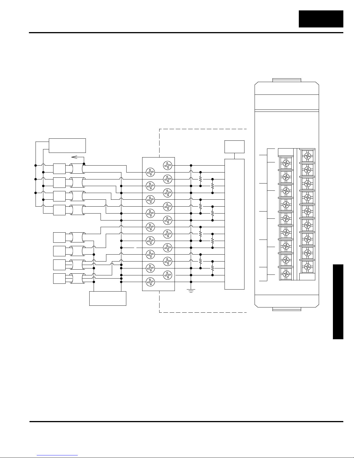
F
3
-
-
0
8
A
D
8
-
C
hanne
l
A
n
alo
gInpu
t
4--
5
F3--08AD 8-Channel Analog Input
Removable
Connector
The F3--08AD module has a removable connector to make wiring easier. Simply
squeeze the top and bottom tabs and gently pull the connector from the module.
Wiring Diagram
Note 1: Terminate all shields at their respective signal source
Note 2: To avoid “ground loop” errors, the following transmitter
types are recommended:
2 & 3 wire: Isolation between input signal & P/S
4 wire: Full isolation between input signal, P/S and
output signal.
+
4 wire 4--20mA
--
Transmitter P/S
See note
4 wire
4--20mA
4 wire
4--20mA
4 wire
4--20mA
4 wire
4--20mA
2 wire
4--20mA
2 wire
4--20mA
3 wire
4--20mA
3 wire
4--20mA
+ --
External P/S
for 4--20mA
Transmitters
(Switching Type DC P/S not recommended)
1+
2+
1--
2--
3+
4+
3--
4--
5+
6+
5--
6--
7+
8+
7--
8--
COM
Internal Module Wiring
COM
1+
2+
1--
2--
3+
4+
3--
4--
5+
6+
5--
6--
7+
8+
7--
8--
COM
250
250
250
250
250
250
250
250
A/D
Analog
Switch
ANALOG INPUT
F3--08AD
4--20mA
C
O
M
+
1
+
--
2
-+
3
+
--
4
--
+
5
+
--
6
-+
7
+
--
8
--
C
O
M
Page 63
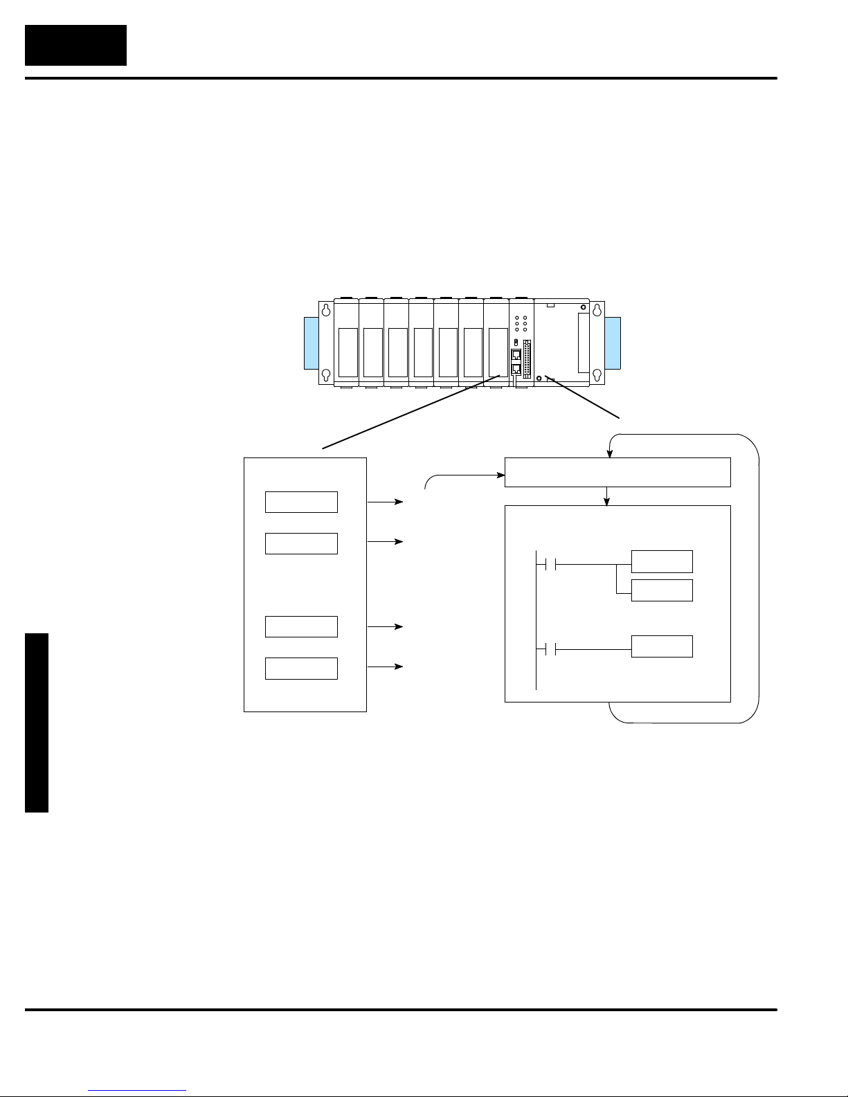
8-ChannelAnalogInpu
t
4--
6
F3--08AD 8-Channel Analog Input
Module Operation
Before you begin writing the control program, it is important to take a few minutes to
understand how the module processes and represents the analog signals.
Channel Scanning
Sequence
The F3--08AD module supplies1 channel of data per each CPU scan. Since there
are eight channels, it can take up to eight scans to get data for all channels. Once all
channels have been scanned the process starts over with channel 1.
You do not have to select all of the channels. Unused channels are not processed, so
if you select only four channels, then the channels will be updated within four scans.
Scan
I/O Update
Channel 1
Channel 2
.
.
.
Channel 8
Channel 1
Even though the channel updates to the CPU are synchronous with the CPU scan,
the module asynchronously monitors the analog transmitter signal and converts the
signal to a 12-bit binary representation. This enables the module to continuously
provide accurate measurements without slowing down the discrete control logic in
the RLL program.
Scan N
Scan N+1
.
.
.
Scan N+7
Scan N+8
Execute Application Program
Read the data
Store data
Page 64
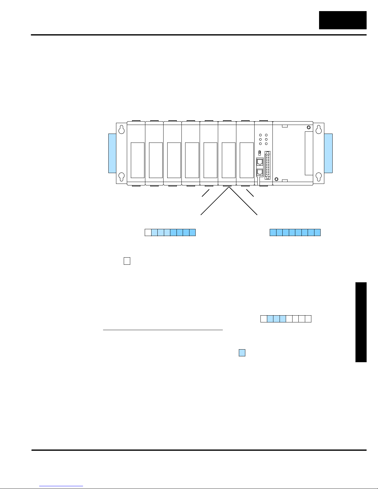
F
3
-
-
0
8
A
D
8
-
C
hanne
l
A
n
alo
gInpu
t
4--
7
F3--08AD 8-Channel Analog Input
F3--08A
D
Understanding the
I/O Assignments
You may recall the F3--08AD module appears to the CPU as a 16-point module.
These 16 points provide:
S an indication of which channel is active.
S the digital representation of the analog signal.
Since all I/O points are automatically mapped into Register (R) memory, it is very
easy to determine the location of the data word that will be assigned to the module.
8pt
Relay
050
057
8pt
Output
Output
040
--
--
047
R 002, R012 R 000, R010
R 011
MSB LSB
8pt
030
--
037
16pt
Input
020
027
-120
127
8ch
(Analog)
010
017
-110
117
16pt
Input
000
007
100
107
--
R 001
MSB LSB
Active Channel
Indication Inputs
1
1
7
1
1
0
0
1
7
0
1
0
-- not used
Within these two register locations, the individual bits represent specific information
about the analog signal.
The next to last three bits of the upper
Register indicate the active channel. The
indicators automatically increment with
MSB LSB
R011
each CPU scan.
Scan Channel Inputs Active Channel
N 000 1
N+1 001 2
N+2 010 3
1
1
1
1
1
1
1
1
1
1
7
6
5
4
3
-- channel indicator inputs
1
1
1
1
1
1
0
2
1
N+3 011 4
N+4 100 5
N+5 101 6
N+6 110 7
N+7 111 8
N+8 000 1
Page 65
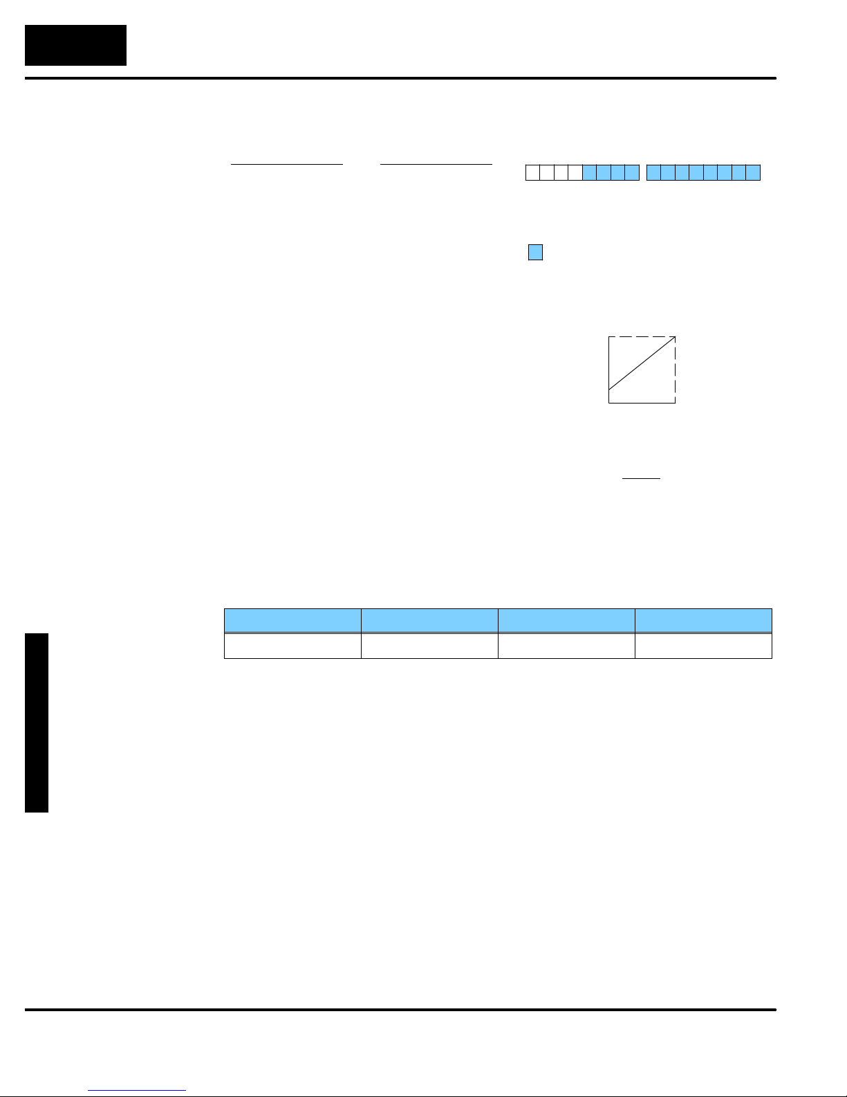
8-ChannelAnalogInpu
t
4--
8
F3--08AD 8-Channel Analog Input
Theremainingtwelvebitsrepresentth
e
Sincethemodulehas12-bitresolution
,
Analog Data Bits
analog data in binary format.
Bit Value Bit Value
0 (LSB) 1 6 64
1 2 7 128
2 4 8 256
3 8 9 512
4 16 10 1024
5 32 11 2048
R011
1
1
1
1
1
1
7
6
5
-- data bits
R001
MSB LSB
1
1
1
1
1
0
0
0
0
0
0
0
1
1
1
1
1
1
1
1
1
1
1
1
4
3
2
1
0
7
6
5
4
3
2
1
0
1
0
the analog signal is converted into 4096
“pieces” ranging from 0 -- 4095 (212). For
example, with a 4 -- 20 mA scale, a 4 mA
4 -- 20mA
20mA
signal would be 0, and a 20 mA signal
would be 4095. This is equivalent to a
4mA
binary value of 0000 0000 0000 to
1111 1111 1111, or 000 to FFF
0 4095
hexadecimal. The following diagram
shows how this relates to each signal
range.
Each “piece” can also be expressed in
Resolution =
H - L
4095
terms of the signal level by using the
equation shown. The following table
shows the smallest signal levels that will
H = high limit of the signal range
L = low limit of the signal range
result in a change in the data value for
each signal range.
Range Highest Signal Lowest Signal Smallest Change
4 to 20mA 20mA 4mA
3.91 µA
Now that you understand how the module and CPU work together to gather and
store the information, you’re ready to write the control program.
Page 66
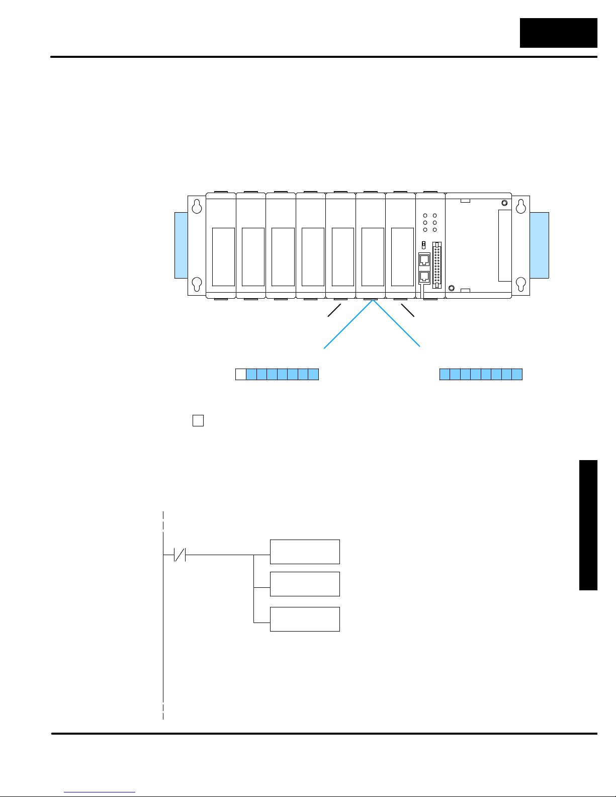
F
3
-
-
0
8
A
D
8
-
C
hanne
l
A
n
alo
gInpu
t
4--
9
Writing the Control Program
F3--08A
D
F3--08AD 8-Channel Analog Input
Identifying the
Data Locations
Since all channels are multiplexed into a single data word, the control program must
be setup to determine which channel is being read. Since the module provides input
points to the CPU, it is very easy to use the active channel status bits to determine
which channel is being monitored.
8pt
Relay
050
--
057
8pt
Output
040
--
047
Output
8pt
030
--
037
16pt
Input
020
027
120
127
(Analog)
--
010
017
110
117
Input
000
007
--
--
100
107
16pt
8ch
R 002, R012 R 000, R010
R 011
MSB LSB
1
1
7
1
1
0
MSB LSB
R 001
0
1
7
0
1
0
-- not used
Single Channel on
Every Scan
The following example shows a program that is designed to read a single channel of
analog data into a Register location on every scan. Once the data is in a Register,
you can perform math on the data, comparethe data againstpreset values, etc. This
example is designed to read channel 1. Since you use jumpers to select the number
of channels to scan, this is the only channel that you can use in this manner.
Read the data
374
DSTR1
R001
BCD F86
DOUT
R400
F51
F60
This rung loads the data into the accumulator on
every scan. (You can use any permissive contact.)
The DL305 CPUs perform math operations in
BCD. This instruction converts the binary data to
BCD. (You can omit this step if your application
does not require the conversion.)
Since the active channel indicators are all off when
channel 1 is being read, you would not have to use
them. (Since you cannot isolate the individual
channels for scanning, channel 1 is the only
channel that can be used in this manner.) The
DOUT instruction moves the data to a storage
register. The BCD value will be stored in R400 and
R401. (Two bytes are required for four digit BCD
numbers.)
Page 67
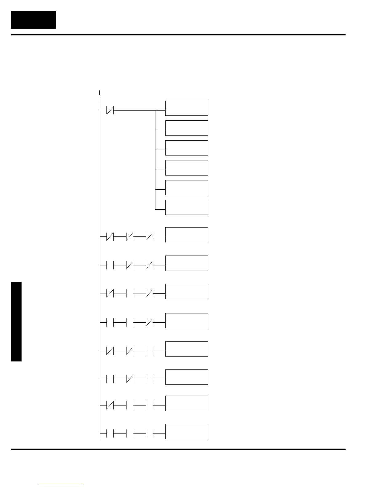
8-ChannelAnalogInpu
t
4--10
F3--08AD 8-Channel Analog Input
Reading Multiple
Channels over
Alternating Scans
The following example shows a program designed to read any of the available
channels of analog data into Register locations. Once the data is in a Register, you
can perform math on the data, compare the data against preset values, etc. Since
the DL305 CPUs use 8-bit word instructions, you have to move the data in pieces. It’s
simple if you follow the example.
Read the data
374
Store channel 1
114
Store channel 2
114 115 116
115 116
DSTR3
R011
DOUT1
R501
DSTR1
R001
DOUT1
R500
DSTR
R500
BCD F86
DOUT
R400
DOUT
R402
F53
F61
F51
F61
F50
F60
F60
This rung loads the four most significant data bits
into the accumulator from Register 011 on every
scan. (You could use any permissive contact.)
Temporarily store the bits to Register 501.
This rung loads the eight least significant data bits
into the accumulator from Register 001.
Temporarily store the bits to Register 500. Since
the most significant bits were loaded into 501, now
R500 and R501 contain all twelve bits in order.
Now that all the bits are stored, load all twelve bits
into the accumulator.
Math operations are performed in BCD. This
instruction converts the binary data to BCD. (You
can omit this step if your application does not
require the conversion.)
The channel indicator inputs are used to let the
CPU know which channel has been loaded into the
accumulator. By using these inputs to control a
DOUT instruction, you can easily move the data to
a storage register. Notice the DOUT instruction
stores the data in two bytes. (Two bytes are
required for four digit BCD numbers.)
Store channel 3
114 115 116
Store channel 4
114
Store channel 5
114 115 116
Store channel 6
114 115 116
Store channel 7
114 115 116
Store channel 8
114 115 116
115 116
DOUT
R404
DOUT
R406
DOUT
R410
DOUT
R412
DOUT
R414
DOUT
R416
F60
F60
F60
F60
F60
F60
Page 68
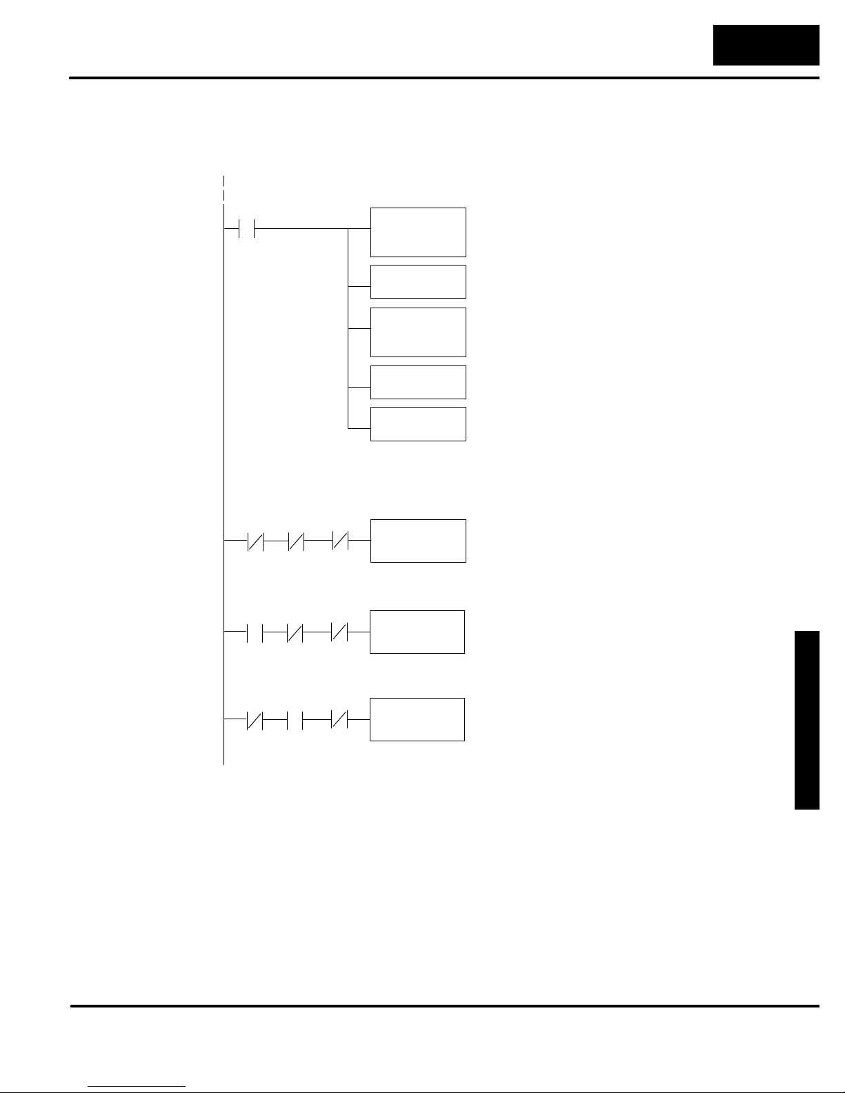
F
3
-
-
0
8
A
D
8
-
C
hanne
l
A
n
alo
gInpu
t
4--11
F3--08AD 8-Channel Analog Input
Reading Multiple
Channels over
Alternating Scans
on a DL350 with a
Conventional
DL305 Base
The example below shows how to read multiple channels on an F3--08AD Analog
module in the 20--27/120--127 address slot. This module must be placed in a 16 bit
slot in order to work.
Load the data
_On
SP1
Channel 1 Select Bit States
LDFK8X120
SHFL
ORFK8X20
ANDD
BCD
K8
Kfff
This rung loads the upper byte of analog data from
the module.
SHFL K8 shifts the data to the left eight places to
make room for the lower byte of data.
The ORF X20 brings the lower byte of data from
the module into the accumulator. At this time there
is a full word of data from the analog module in the
accumulator.
The ANDD Kfff masks off the twelve least
significant bits of data from the word. This is the
actual analog value.
The BCD command converts the data to BCD
format.
X125X124 X126
Channel 2 Select Bit States
X125X124 X126
Channel 3 Select Bit States
X125X124 X126
OUT
OUT
V3001
OUT
V3002
This writes channel one analog data to V3000
when bits X124, X125 and X126 are as shown.
V3000
This writes channel two analog data to V3001
when bits X124, X125 and X126 are as shown.
This writes channel three analog data to V3002
when bits X124, X125 and X126 are as shown.
Page 69
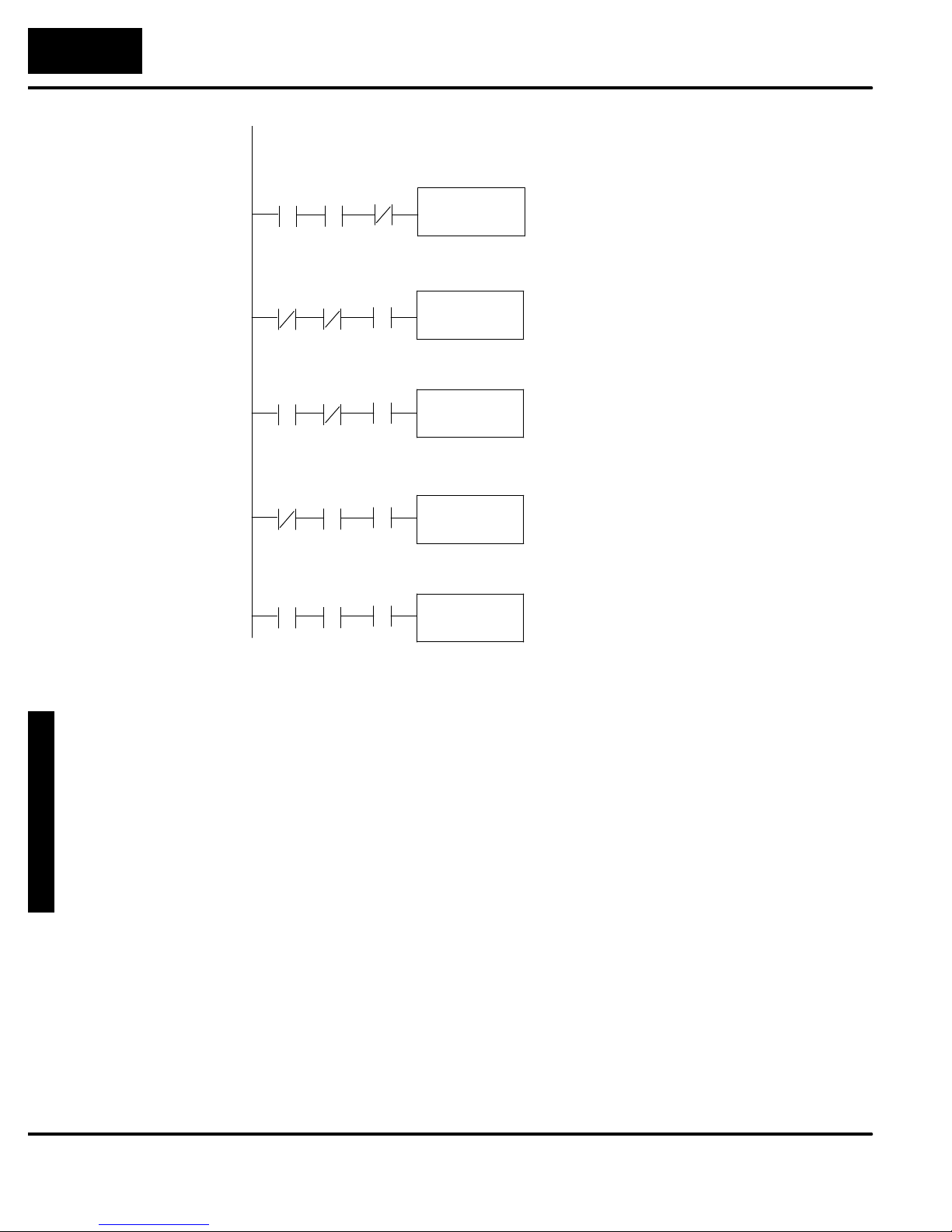
8-ChannelAnalogInpu
t
4--12
F3--08AD 8-Channel Analog Input
Channel 4 Select Bit States
X125X124 X126
Channel 5 Select Bit States
X125X124 X126
Channel 6 Select Bit States
X125X124 X126
Channel 7 Select Bit States
X125X124 X126
OUT
OUT
V3004
OUT
V3005
OUT
V3006
V3003
This writes channel four analog data to V3003
when bits X124, X125 and X126 are as shown.
This writes channel five analog data to V3004
when bits X124, X125 and X126 are as shown.
This writes channel six analog data to V3005 when
bits X124, X125 and X126 are as shown.
This writes channel seven analog data to V3006
when bits X124, X125 and X126 are as shown.
Channel 8 Select Bit States
X125X124 X126
OUT
V3007
This writes channel eight analog data to V3007
when bits X124, X125 and X126 are as shown.
Page 70

F
3
-
-
0
8
A
D
8
-
C
hanne
l
A
n
alo
gInpu
t
4--13
F3--08AD 8-Channel Analog Input
Thefollowingexampleshowshowyo
u
Scaling the Input
Data
Most applications usually require
measurements in engineering units,
which provide more meaningful data.
This is accomplished by using the
conversion formula shown.
would use the analog data to represent
pressure (PSI) from 0 to 100. This
example assumes the analog value is
1760. This should yield approximately
42.9 PSI.
Units =
Units = value in Engineering Units
A = Analog value (0 -- 4095)
S = high limit of the Engineering
unit range
A
S
4096
Units =
Units =
Units = 42.9
4096
1760
4096
A
S
100
Page 71
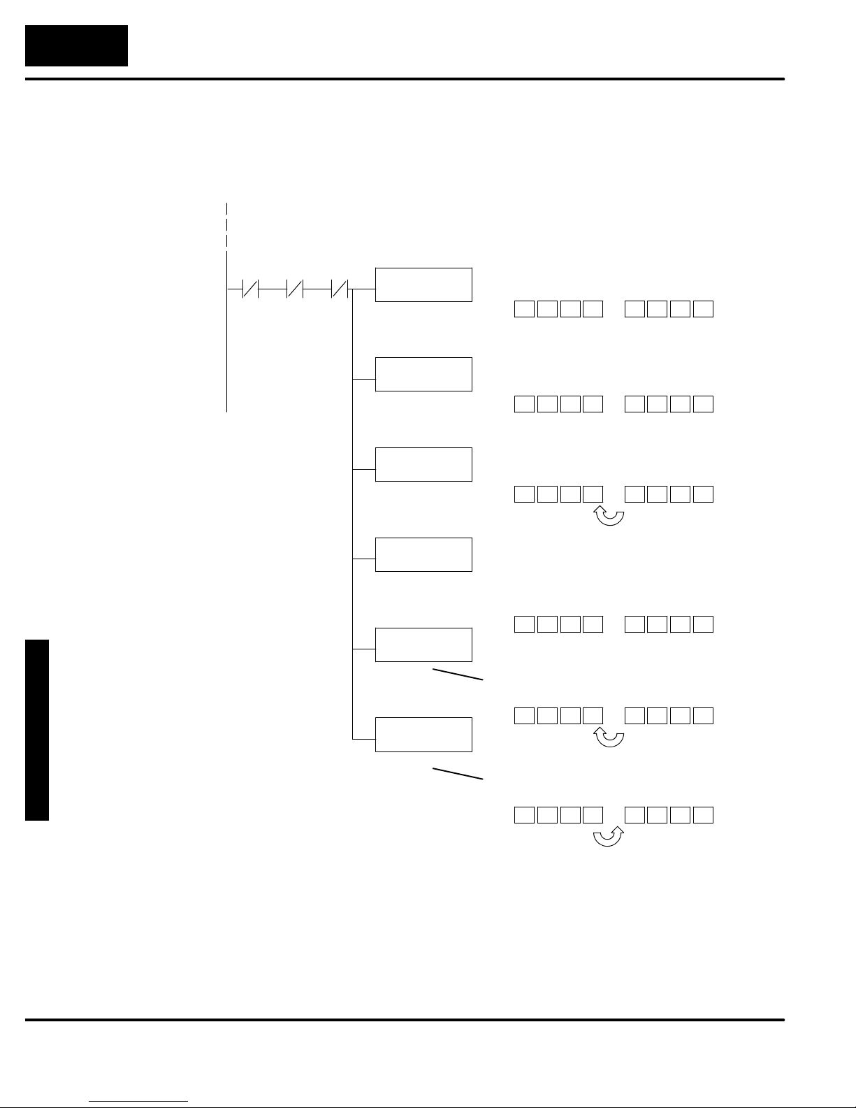
8-ChannelAnalogInpu
t
4--14
F3--08AD 8-Channel Analog Input
The following instructions are required to scale the data. We’ll continue to use the
42.9 PSI example. In this example we’re using channel 1. Input 114, input 115, and
input 116 are all off when channel 1 data is being read. Of course, if youwere using a
different channel, you would use the active channel indicator point combination that
corresponds to the channel you were using.
This example assumes you have already read the analog data
and stored the BCD equivalent in R400 and R401
Scale the data
114 115 116
DSTR
R400
F50
This instruction brings the analog value (in BCD)
into the accumulator.
Accumulator
1 7 6 0
Aux. Accumulator
0 0 0 0
R577 R576
DIV
K4096
DSTR
R576
MUL
K100
DSTR
R576
DOUT
R450
F74
F50
F73
F50
F60
The analog value is divided by the resolution of the
module, which is 4096. (1760 / 4096 = 0.4296)
Accumulator
0 0 0 0
This instruction moves the two-byte decimal
portion into the accumulator for further operations.
Accumulator
4 2 9 6
The accumulator is then multiplied by the scaling
factor, which is 100. (100 x 4296 = 429600). Notice
the most significant digits are now stored in the
auxilliary accumulator. (This is different from the
way the Divide instruction operates.)
Accumulator
9 6 0 0
This instruction moves the two-byte auxilliary
accumulator for further operations.
Accumulator
0 0 4 2
This instruction stores the accumulator to R450
and R451. R450 and R451 now contain the PSI,
which is 42 PSI.
Accumulator
0 0 4 2
Aux. Accumulator
4 2 9 6
R577 R576
Aux. Accumulator
4 2 9 6
R577 R576
Aux. Accumulator
0 0 4 2
R577 R576
Aux. Accumulator
0 0 4 2
R577 R576
Store in R451 & R450
0 0 4 2
R451 R450
Page 72
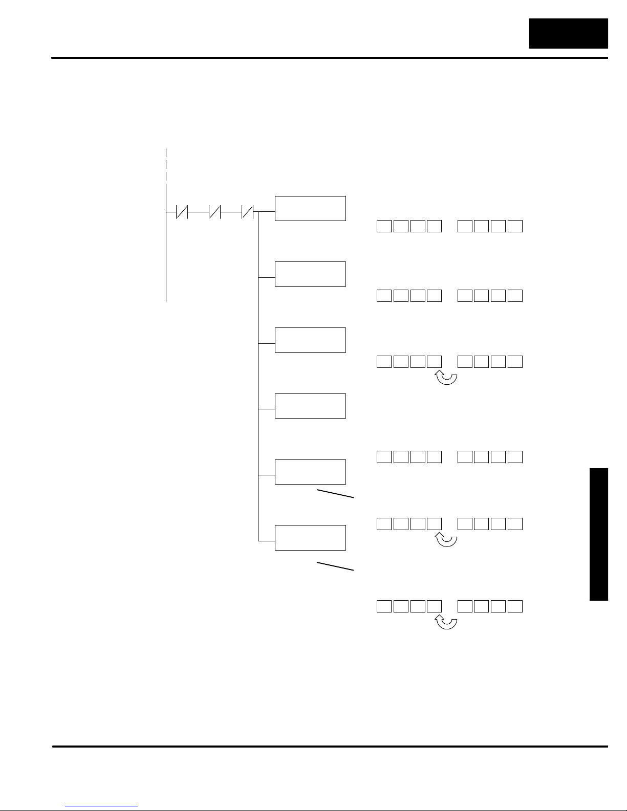
F
3
-
-
0
8
A
D
8
-
C
hanne
l
A
n
alo
gInpu
t
4--15
F3--08AD 8-Channel Analog Input
You probably noticed the previous example yielded 42 PSI when the real value
should have been 42.9 PSI. By changingthe scalingvalue slightly, we can “imply” an
extra decimal of precision. Notice in the following example we’ve added another digit
to the scale. Instead of a scale of 100, we’re using 1000, which implies 100.0 for the
PSI range.
This example assumes you have already read the analog data
and stored the BCD equivalent in R400 and R401
Scale the data
114 115 116
DSTR
R400
F50
This instruction brings the analog value (in BCD)
into the accumulator.
Accumulator
1 7 6 0
Aux. Accumulator
0 0 0 0
R577 R576
DIV
K4096
DSTR
R576
MUL
K1000
DSTR
R576
DOUT
R450
F74
F50
F73
F50
F60
The analog value is divided by the resolution of the
module, which is 4096. (1760 / 4096 = 0.4296)
Accumulator
0 0 0 0
This instruction moves the two-byte decimal
portion into the accumulator for further operations.
Accumulator
4 2 9 6
The accumulator is multiplied by the scaling factor,
which is now 1000. (1000 x 4296 = 4296000). The
most significant digits are now stored in the
auxilliary accumulator. (This is different from the
way the Divide instruction operates.)
Accumulator
6 0 0 0
This instruction moves the two-byte auxilliary
accumulator for further operations.
Accumulator
0 4 2 9
Aux. Accumulator
4 2 9 6
R577 R576
Aux. Accumulator
4 2 9 6
R577 R576
Aux. Accumulator
0 4 2 9
R577 R576
Aux. Accumulator
0 4 2 9
R577 R576
This instruction stores the accumulator to R450
and R451. R450 and R451 now contain the PSI,
which implies 42.9.
Accumulator
0 4 2 9
Store in R451 & R450
0 4 2 9
R451 R450
Page 73
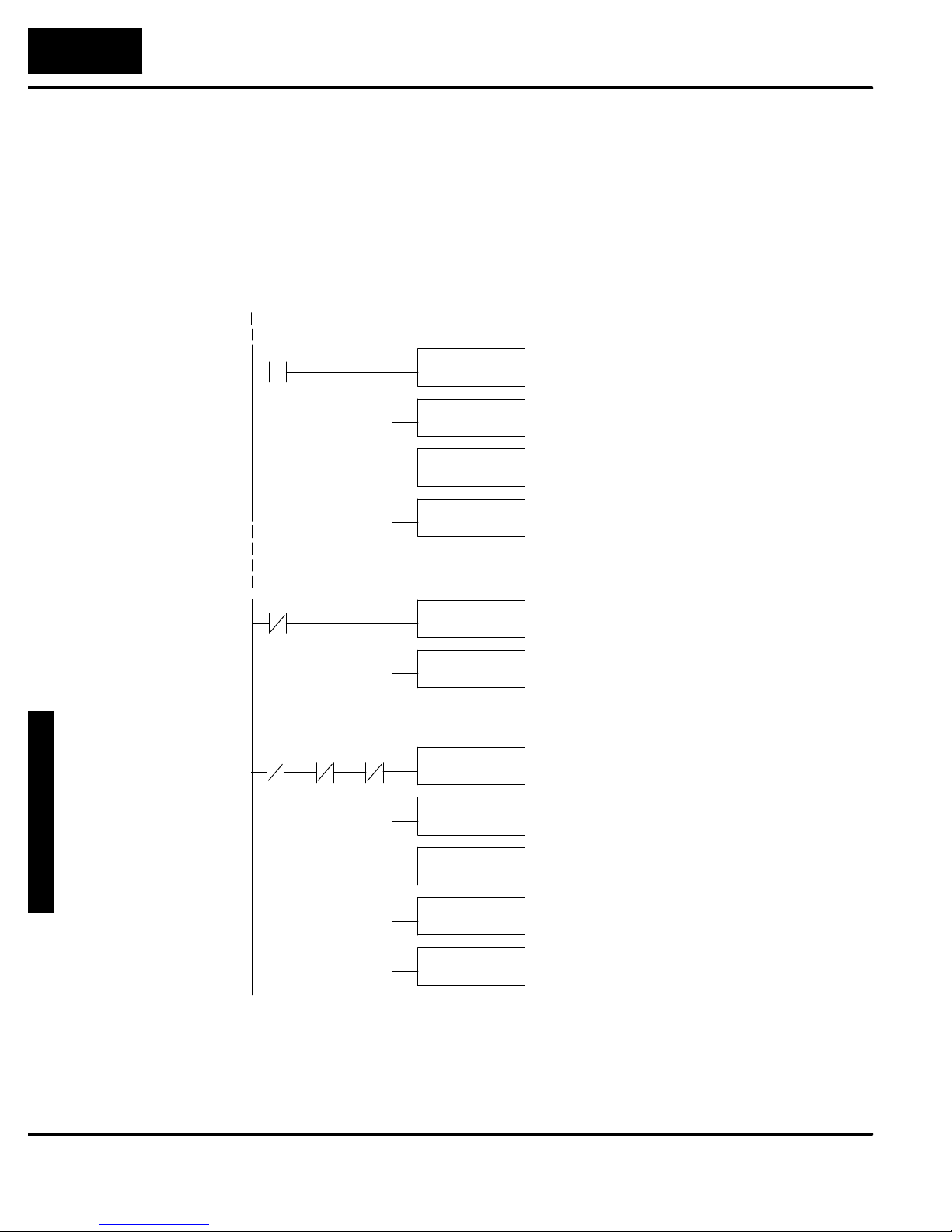
8-ChannelAnalogInpu
t
4--16
F3--08AD 8-Channel Analog Input
This example program shows how you can use the instructions to load these
equation constants into data registers. The example was written for channel 1, but
you could easily use a similar approach to use different scales for all channels if
required.
You could just use the appropriate constants in the instructions dedicated for each
channel, but this method allows easier modifications. For example, you could easily
use an operator interface or a programming device to change the constants if they
are stored in Registers.
Load the constants
374
DSTR
K4096
F50
On the first scan, these first two instructions load
the analog resolution (constant of 4096) into R430
and R431.
Read the data
374
Store channel 1
114 115 116
DOUT
R430
DSTR
K1000
DOUT
R432
DSTR3
R011
DOUT1
R501
DIV
R430
DSTR
R576
MUL
R432
F60
F50
F60
F53
F61
F74
F50
F73
These two instructions load the high limit of the
Engineering unit scale (constant of 1000) into
R432 and R433. Note, if you have different scales
for each channel, you’ll also have to enter the
Engineering unit high limit for those as well.
This rung loads the four most significant data bits
into the accumulator from Register 011 on every
scan. (You could use any permissive contact.)
Temporarily store the bits to Register 501.
The analog value is divided by the resolution of the
module, which is stored in R430.
This instruction moves the decimal portion from the
auxilliary accumulator into the regular accumulator
for further operations.
The accumulator is multiplied by the scaling factor,
which is stored in R432.
DSTR
R576
DOUT
R400
F50
F60
This instruction moves most significant digits (now
stored in the auxilliary accumulator) into the
regular accumulator for further operations.
The scaled value is stored in R400 and R401 for
further use.
Page 74
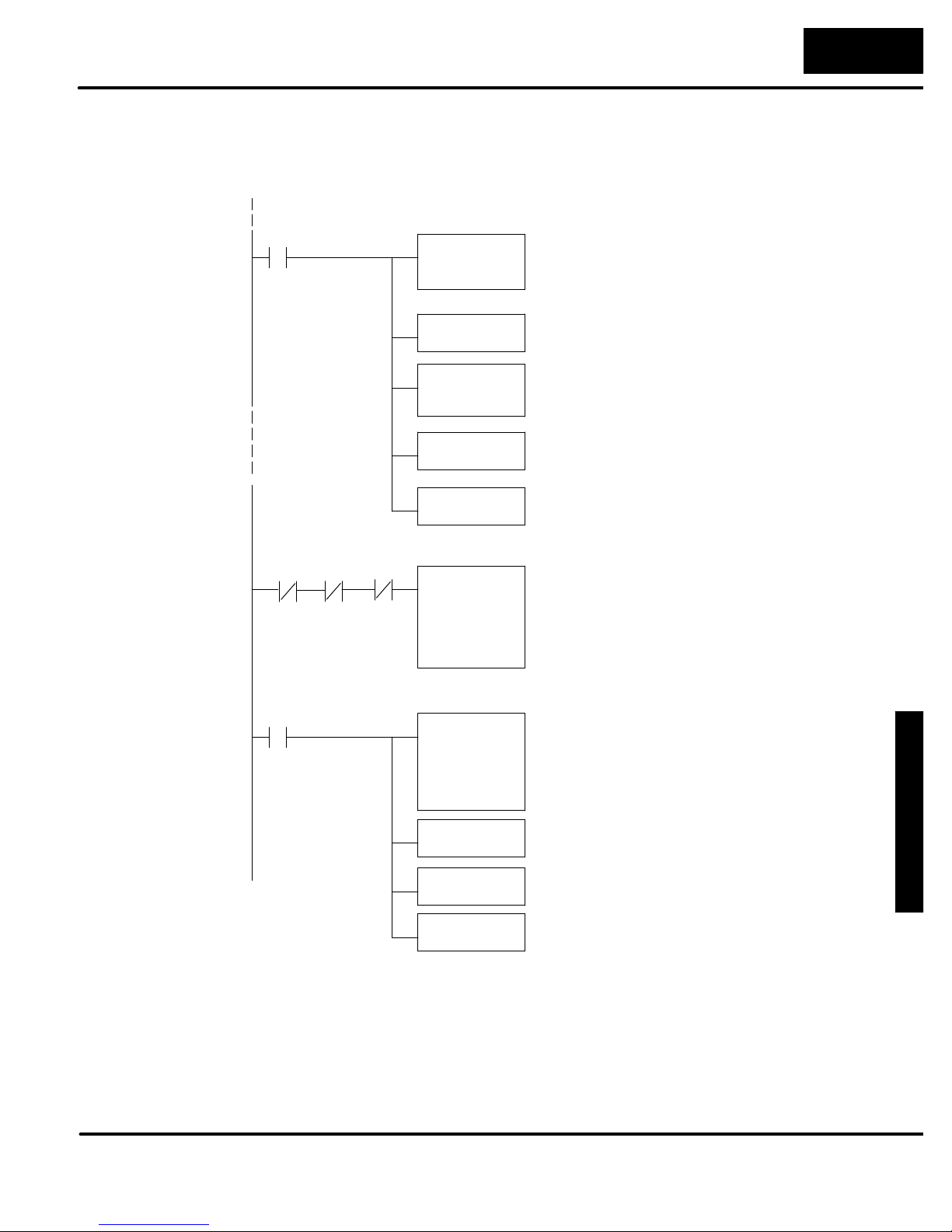
F
3
-
-
0
8
A
D
8
-
C
hanne
l
A
n
alo
gInpu
t
4--17
F3--08AD 8-Channel Analog Input
Scaling on a DL350
with a
Conventional
DL305 Base
The example below shows how to scale input datafrom an F3--08AD Analog module
in the 20--27/120--127 address slot. This module must be placed in a 16 bit slot in
order to work.
Load the data
_On
SP1
Select Channel 1
X125
X124 X126
Scale the data
_On
SP1
LDFK8X120
SHFL K8
ORF
ANDD Kfff
BCD
OUT
Channel 1
Analog Data
Register (BCD)
LD
Channel 1
Analog Data
Register (BCD)
X20
K8
V3001
V3000
This loads the upper byte of the analog data from
the module.
SHFL K8 shifts the data to the left eight places to
make room for the lower byte of data.
The ORF X20 brings the lower byte of data from
the module into the accumulator. At this time there
is a full word of data from the analog module in the
accumulator.
The ANDD Kfff masks off the twelve least
significant bits of data from the word. This is the
actual analog value.
The BCD command converts the data to BCD
format.
The bits X124, X125 and X126, all OFF, selects
channel one. This rung puts the data from the
analog module into the respective V--memory
location.
Rung 3 scales a 0 to 200 range of a transducer
over the 4096 counts. The raw analog value is
loaded to the accumulator from V3000
(Channel #1).
MUL K2000
DIV K4096
OUT V3010
It is then multiplied by 2000. The additional zero
provides a higher degree of resolution.
It is then divided by 4096, which is the resolution of
the module.
The scaled value is stored in V3010 with an
implied decimal.
Page 75

8-ChannelAnalogInpu
t
4--18
F3--08AD 8-Channel Analog Input
Analog and Digital
Value Conversions
Sometimes it is helpful to be able to quickly convert between the signal levels and the
digital values. This is especially helpful during machine startup or troubleshooting.
The following table provides formulas to make this conversion easier.
Range If you know the digital value ... If you know the analog signal
level ...
4 to 20mA
A =
16D
4095
+ 4
For example, if you have measured the
signal at 10mA, you would use the
D =
D =
4095
4095
16
16
(A - 4)
(A - 4)
following formula to determine the digital
value that should be stored inthe register
location that contains the data.
4095
D =
D = (255.93) (6)
D = 1536
(10mA - 4)
16
Now you have all the necessary information to get your analog module installed and
operating correctly!
Page 76

1
5
F3--16AD
16-Channel
Analog Input
In This Chapter. . . .
— Module Specifications
— Setting the Module Jumpers
— Connecting the Field Wiring
— Module Operation
— Writing the Control Program
Page 77

16-ChannelAnalogInput
5--
2
F3--16AD 16-Channel Analog Input
Module Specifications
The following table provides the specifications for the F3--16AD Analog Input
Module from FACTS Engineering. Review these specifications to make sure the
module meets your application requirements.
Number of Channels 16, single ended (one common)
Input Ranges ? 5V, ? 10V, 0--5V1, 0--10V,
0--20 mA, 4 -- 20 mA
Resolution 12 bit (1 in 4096)
Input Impedance 2MO , voltage input
500O ? 1%, current input
Absolute Maximum Ratings ? 25V, voltage input
? 30 mA, current input
Conversion Time
Converter Type Successive Approximation, AD574
Linearity Error ? 1 count maximum
Maximum Inaccuracy at 77 °F
(25 °C)
Accuracy vs. Temperature
Recommended Fuse 0.032 A, Series 217 fast-acting, current inputs
Power Budget Requirement 33 mA @ 9 VDC, 47 mA @ 24 VDC
External Power Supply None required
Operating Temperature
Storage Temperature
35µs per channel
1 channel per CPU scan
0.25% of full scale, voltage input
1.25% of full scale, current input
57 ppm / _C maximum full scale
32° to 140° F (0° to 60_ C)
--4° to 158° F (--20° to 70_ C)
2
Analog Input
Configuration
Requirements
Relative Humidity 5 to 95% (non-condensing)
Environmental air No corrosive gases permitted
Vibration MIL STD 810C 514.2
Shock MIL STD 810C 516.2
Noise Immunity NEMA ICS3--304
1 -- requires gain adjustment with potentiometer.
2 -- resolution is 3275 counts (instead of 4096). Allows easier broken transmitter detection
The F3--16AD Analog Input appears as a 16-point module. The module can be
installed in any slot configured for 16 points. See the DL305 User Manual for details
on using 16 point modules in DL305 systems. The limitation onthe number ofanalog
modules are:
S For local and expansion systems, the available power budget and
16-point module usage are the limiting factors.
Page 78
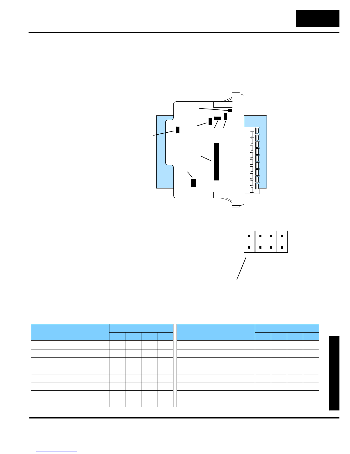
F
3
-
-
1
6
A
D
1
6
-
C
hanne
l
A
n
alo
gInpu
t
5--
3
Setting the Module Jumpers
Channel(s
)
Channel(s
)
F3--16AD 16-Channel Analog Input
Jumper Locations
Selecting the
Number of
Channels
The module is set atthe factory for a 0--20 mA signal on all sixteen channels. If this is
acceptable you do not have to change any of the jumpers. The following diagram
shows the jumper locations.
ADJ
10V
Polarity
Bipolar
Unipolar
Span
20V
Current
Channels
8
4
2
1
Gain
X100
X1000
Gain
X1
X10
If you examine the rear of the module,
you’ll notice several jumpers. The
+8 +4 +2
+1
jumpers labeled +1, +2, +4 and +8 are
used to select the number of channels
that will be used. Without any jumpers
the module processes one channel. By
installing the jumpers you can add
channels. The module is set from the
Number of
Channels
factory for sixteen channel operation.
Any unused channels are not processed
so if you only select channels 1--8, then
Jumpers installed as shown
selects 16-channel operation
the last eight channels will not be active.
The following table shows which jumpers
to install.
Jumper
+8 +4 +2 +1
1 No No No No 1 2 3 4 5 6 7 8 9 Yes No No No
1 2 No No No Yes 1 2 3 4 5 6 7 8 9 10 Yes No No Yes
1 2 3 No No Yes No 1 2 3 4 5 6 7 8 9 10 11 Yes No Yes No
1 2 3 4 No No Yes Yes 1 2 3 4 5 6 7 8 9 10 11 12 Yes No Yes Yes
1 2 3 4 5 No Yes No No 1 2 3 4 5 6 7 8 9 10 11 12 13 Yes Yes No No
1 2 3 4 5 6 No Yes No Yes 1 2 3 4 5 6 7 8 9 10 11 12 13 14 Yes Yes No Yes
1 2 3 4 5 6 7 No Yes Yes No 1 2 3 4 5 6 7 8 9 10 11 12 13 14 15 Yes Yes Yes No
1 2 3 4 5 6 7 8 No Yes Yes Yes 1 2 3 4 5 6 7 8 9 10 11 12 13141516 Yes Yes Yes Yes
Jumper
+8 +4 +2 +1
Page 79
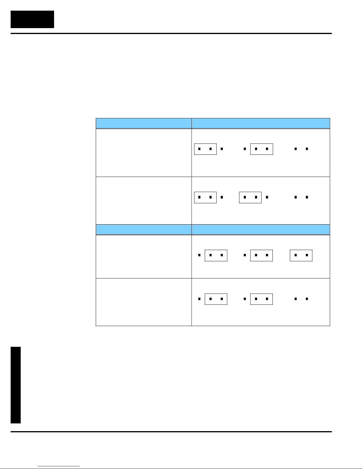
16-ChannelAnalogInput
5--
4
F3--16AD 16-Channel Analog Input
Selecting Input
Signal Ranges
As you examined the jumper settings, you may have noticed there are current
jumpers for each individual channel. These jumpers allow you to select the type of
signal (voltage or current).
The span and polarity jumpers are used to select the signal range. The polarity and
span selection affect all the channels. For example, if you select unipolar operation
and a 10V span, you can use both 0 --10V and 0--20 mA signals at the same time.
Channels that will receive 0--20 mA signalsshould have thecurrent jumper installed.
The following table shows the jumper selections for the various ranges. (Only
channel 1 is used in the example, but all channels must be set.)
Bipolar Signal Range Jumper Settings
--5 VDC to +5 VDC
--10 VDC to +10 VDC
Polarity
UniBi
Polarity
UniBi
Span
Span
10V20V
Current Jumper
Current Jumper
10V20V
Unipolar Signal Range Jumper Settings
0 to 20 mA
(these settings are also used
Polarity
UniBi
Span
for the 4--20mA range)
0 VDC to +10 VDC
Polarity
Span
UniBi
10V20V
Current Jumper
Current Jumper
10V20V
Page 80
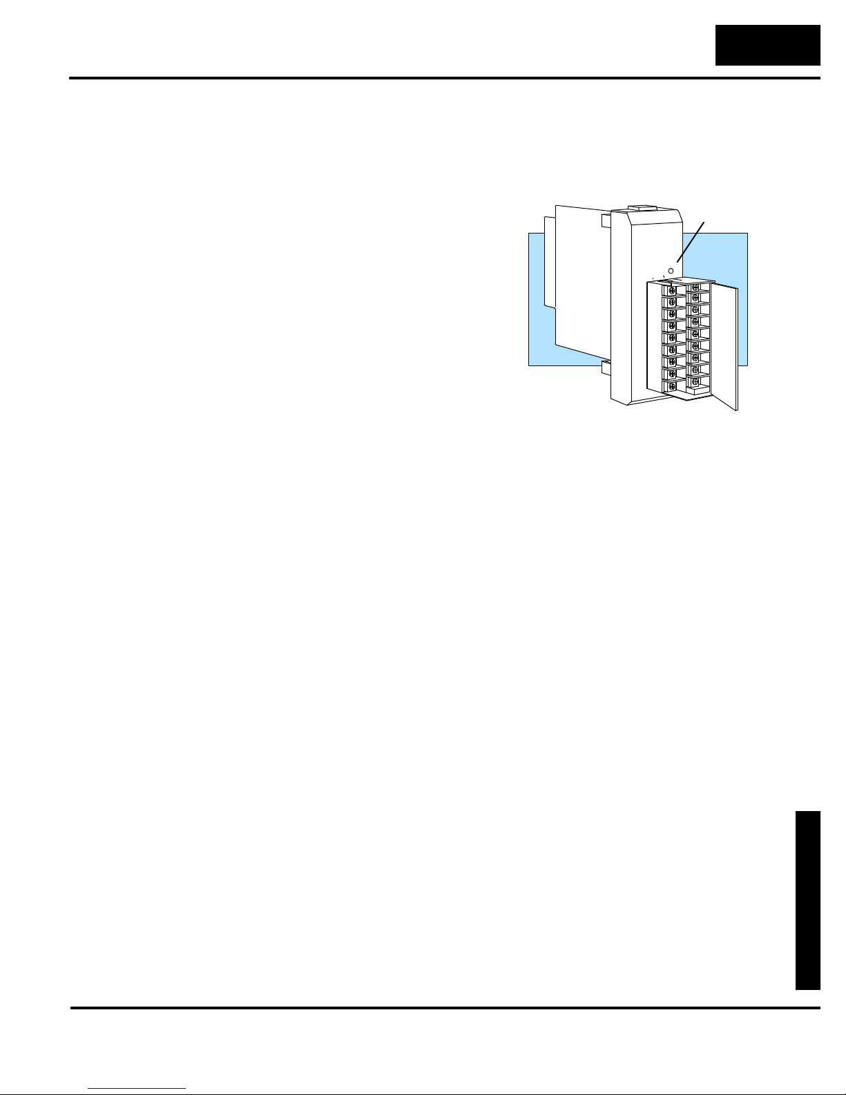
F
3
-
-
1
6
A
D
1
6
-
C
hanne
l
A
n
alo
gInpu
t
5--
5
F3--16AD 16-Channel Analog Input
Gain Jumpers
Variable Gain
Adjustment
You do not have to change the Gain jumpers. These jumpers are installed to allow
the ranges shown previously. Note, if you change these jumpers the module will not
operate the way you expect.
If you look at the terminal block closely,
you’ll notice a small hole conceals an
adjustment potentiometer. This small
potentiometer is used to adjust the gain
for certain situations.
For example, if you have 0--5V
transmitters you have to use the 0--10V
scale on the module. Since the module
converts the signal to a digital value
between 0 and 4095, a 5V signal would
only yield a value of 2048. Fortunately,
the variable gain feature provides a
simple solution. Just complete the
following steps.
1. Install a jumper on the gain adjustment pins. (This jumper location is
labeled ADJ.)
2. Apply 5V to one of the channels.
3. Use a handheld programmer or DirectSOFT to monitor the input register
that contains the analog data. (If you’re not familiar with this procedure, wait
until you read the section on Writing the Control Program. This will show
you how to get data into a register. You can come back to this procedure
later.)
4. Adjust the potentiometer until the register value reads 4094 or 4095. The
potentiometer is turned clockwise to increase the gain.
Potentiometer
Adjustment
Hole
Now the module has been adjusted so a 5V signal provides a digital value of 4095
instead of 2048.
Page 81

16-ChannelAnalogInput
5--
6
F3--16AD 16-Channel Analog Input
Connecting the Field Wiring
Wiring Guidelines
User Power Supply
Requirements
Your company may have guidelines for wiring and cable installation. If so, you should
check those before you begin the installation. Here are some general things to
consider.
S Use the shortest wiring route whenever possible.
S Use shielded wiring and ground the shield at the signal source. Do not
ground the shield at both the module and the source.
S Don’t run the signal wiring next to large motors, high current switches, or
transformers. This may cause noise problems.
S Route the wiring through an approved cable housing to minimize the risk
of accidental damage. Check local and national codes to choose the
correct method for your application.
The F3--16AD receives all power from the base. A separate power supply is not
required.
Page 82
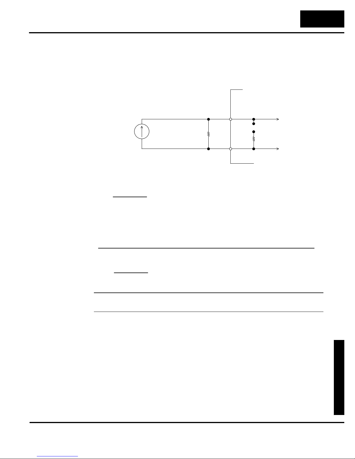
F
3
-
-
1
6
A
D
1
6
-
C
hanne
l
A
n
alo
gInpu
t
5--
7
F3--16AD 16-Channel Analog Input
Custom Input
Ranges
Occasionally you may have the need to connect a transmitter with an unusual signal
range. By changing the wiring slightly and adding an external resistor to convert the
current to voltage, you can easily adapt this module to meet the specifications for a
transmitter that does not adhere to one of the standard input ranges. The following
diagram shows how this works.
Internal
Module
Circuitry
+CH1
R
COM
Jumper
Removed
250O
V
max
+
--
50mA
Current
Transmitter
R =
I
max
R = value of external resistor
V
= high limit of selected voltage range
max
I
= maximum current supplied by the transmitter
max
Example: current transmitter capable of 50mA, 0 -- 10V range selected.
10V
R =
R = 200 ohms
50mA
NOTE: Your choice of resistor can affect the accuracy of the module. A resistor that
has ? 0.1% tolerance and a ? 50ppm / _C temperature coefficient is recommended.
Page 83
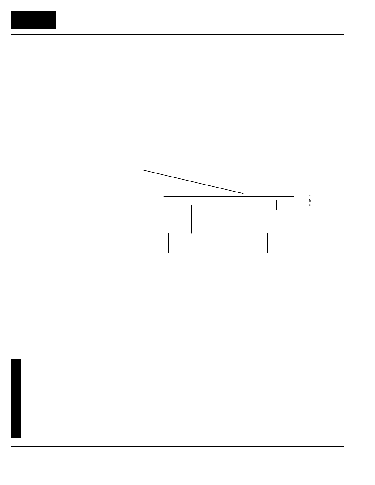
16-ChannelAnalogInput
5--
8
F3--16AD 16-Channel Analog Input
Current Loop
Transmitter
Impedance
Standard 4 to 20 mA transmitters and transducers can operate froma wide variety of
power supplies. Not all transmitters are alike and the manufacturers often specify a
minimum loop or load resistance that must be used with the transmitter at the various
voltages.
The F3--16AD provides 500 ohm resistance for each channel. If your transmitter
requires a load resistance below 500 ohms, then you do not have to make any
adjustments. However, if your transmitter requires a load resistancehigher than 500
ohms, then you need to add a resistor in series with the module.
Consider the following example for a transmitter being operated from a 36 VDC
supply with a recommended load resistance of 750 ohms. Since the module has a
500 ohm resistor, you need to add an additional resistor.
R = Tr - Mr
R = 750 - 500
R = 250
DC Supply
0V
+36V
R -- Resistor to add
Tr -- Transmitter Requirement
Mr -- Module resistance (internal 500 ohms)
Module Channel 1
R
--
+
500O
+ --
Two-wire Transmitter
Page 84
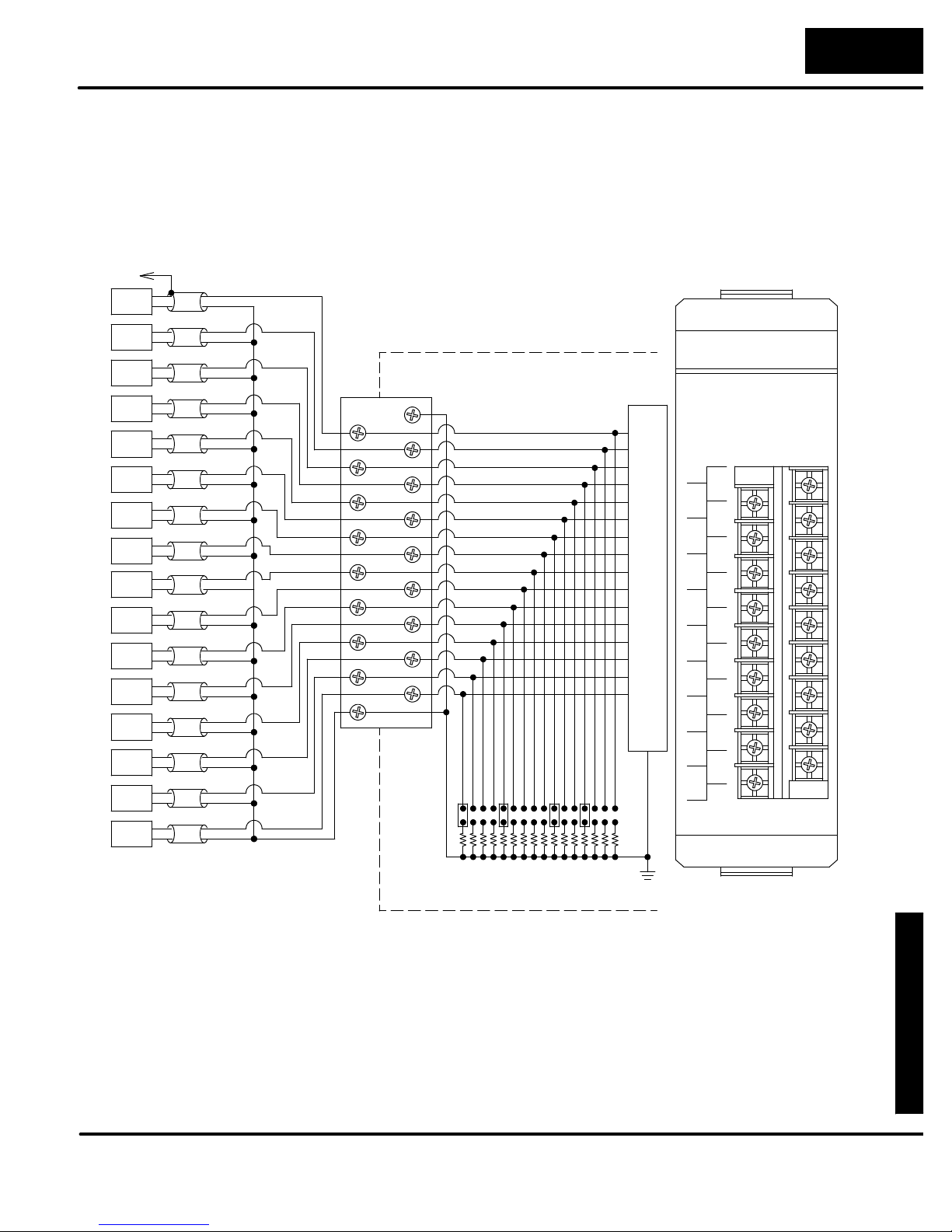
F
3
-
-
1
6
A
D
1
6
-
C
hanne
l
A
n
alo
gInpu
t
5--
9
F3--16AD 16-Channel Analog Input
Note1:Terminateallshieldsattheirrespectivesignalsource.
Removable
Connector
The F3--16AD module has a removable connector to make wiring easier. Simply
squeeze the top and bottom tabs and gently pull the connector from the module.
Wiring Diagram
Note 2: Jumpers for CH4, 7, 12 and 16 are installed for current input.
See note
CH1
CH2
CH3
CH4
CH5
CH6
CH7
CH8
CH9
CH10
CH11
CH12
CH13
CH14
CH15
CH16
Volatage
Transmitter
Volatage
Transmitter
Volatage
Transmitter
Current
Transmitter
Volatage
Transmitter
Volatage
Transmitter
Current
Transmitter
Volatage
Transmitter
Volatage
Transmitter
Volatage
Transmitter
Volatage
Transmitter
Current
Transmitter
Volatage
Transmitter
Volatage
Transmitter
Volatage
Transmitter
Current
Transmitter
+
+
+
+
+
+
+
+
+
+
+
+
+
+
+
+
1
3
5
7
9
11
13
15
COM
COM
2
4
6
8
10
12
14
16
Internal Module Wiring
Analog
Switch
ANALOG INPUT
F3--16AD
C
O
M
CH
1
CH
CH
2
3
CH
4
CH
5
CH
6
CH
CH
7
CH
8
9
CH
CH
10
11
CH
CH
12
13
CH
CH
14
15
CH
C
16
O
M
All resistors are 500O
Page 85
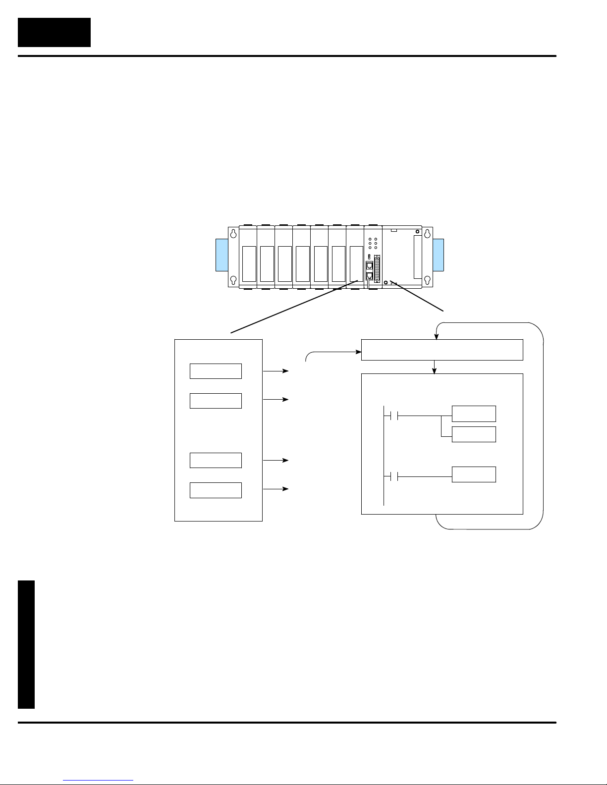
16-ChannelAnalogInput
5--10
F3--16AD 16-Channel Analog Input
Module Operation
Before you begin writing the control program, it is important to take a few minutes to
understand how the module processes and represents the analog signals.
Channel Scanning
Sequence
The F3--16AD module supplies 1 channel of data per each CPU scan. Since there
are sixteen channels, it can take up to sixteen scans to get data for all channels.
Once all channels have been scanned the process starts over with channel 1.
You do not have to select all of the channels. Unused channels are not processed, so
if you select only eight channels, then the channels will be updated within eight
scans.
Scan
I/O Update
Channel 1
Scan N
Execute Application Program
Channel 2
.
.
.
Channel 16
Channel 1
Scan N+1
.
.
.
Scan N+15
Scan N+16
Read the data
Store data
Even though the channel updates to the CPU are synchronous with the CPU scan,
the module asynchronously monitors the analog transmitter signal and converts the
signal to a 12-bit binary representation. This enables the module to continuously
provide accurate measurements without slowing down the discrete control logic in
the RLL program.
Page 86
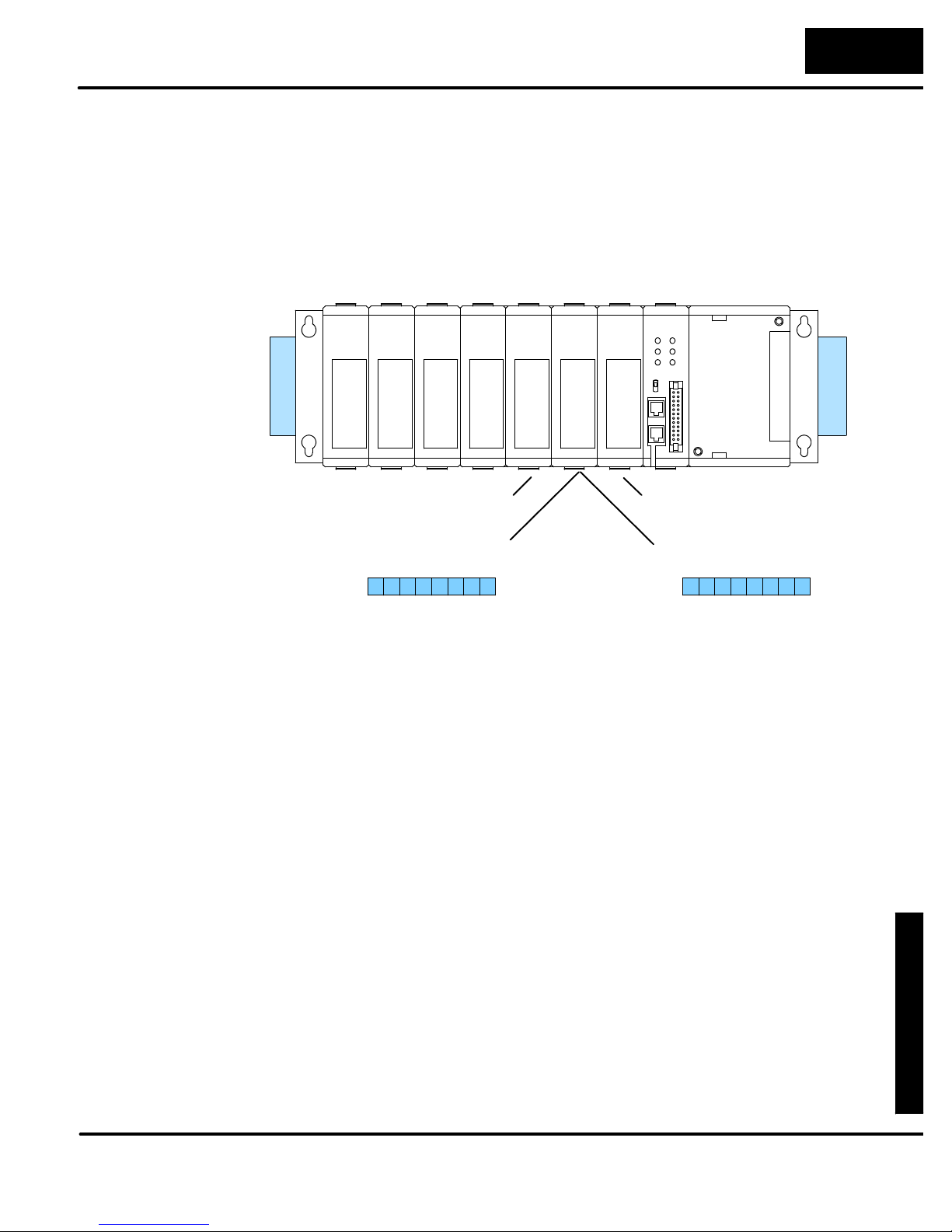
F
3
-
-
1
6
A
D
1
6
-
C
hanne
l
A
n
alo
gInpu
t
5--11
F3--16AD 16-Channel Analog Input
F3--16A
D
Understanding the
I/O Assignments
You may recall the F3--16AD module appears to the CPU as a 16-point module.
These 16 points provide:
S an indication of which channel is active.
S the digital representation of the analog signal.
Since all I/O points are automatically mapped into Register (R) memory, it is very
easy to determine the location of the data word that will be assigned to the module.
8pt
Relay
050
057
8pt
Output
Output
040
--
--
047
R 002, R012 R 000, R010
R 011
MSB LSB
8pt
030
--
037
16pt
Input
020
027
120
127
010
017
-110
117
16pt
Input
000
007
100
107
--
16ch
(Analog)
--
R 001
MSB LSB
1
1
7
1
1
0
0
1
7
0
1
0
Within these two register locations, the individual bits represent specific information
about the analog signal.
Page 87

16-ChannelAnalogInput
5--12
F3--16AD 16-Channel Analog Input
Active Channel
Indicator Inputs
The last four inputs of the upper Register
indicate the active channel. The
indicators automatically increment with
each CPU scan.
Channel Active
Scan Inputs Channel
N 0000 1
N+1 0001 2
N+2 0010 3
N+3 0011 4
N+4 0100 5
N+5 0101 6
N+6 0110 7
N+7 0111 8
N+8 1000 9
N+9 1001 10
N+10 1010 11
N+11 1011 12
N+12 1100 13
N+13 1101 14
N+14 1110 15
N+15 1111 16
R011
MSB LSB
1
1
1
1
1
1
1
1
1
1
7
6
5
4
3
1
1
1
1
1
1
0
2
1
-- channel indicator inputs
Page 88
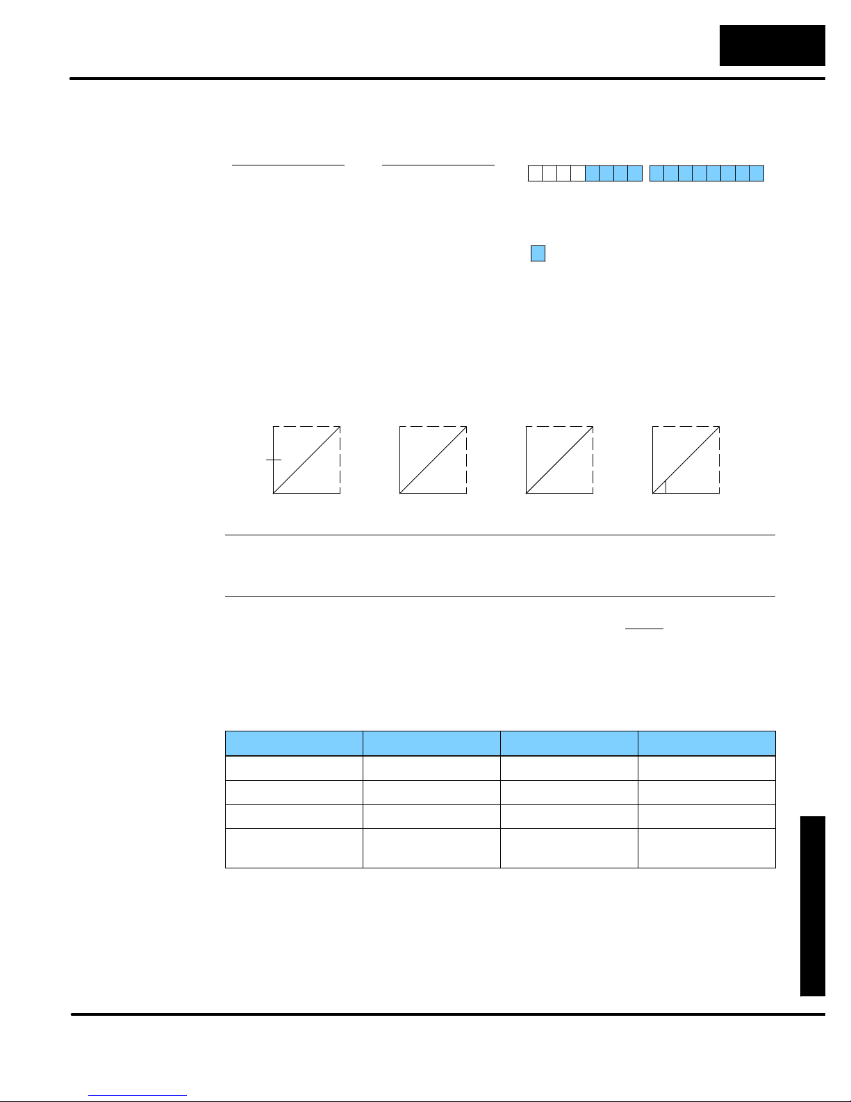
F
3
-
-
1
6
A
D
1
6
-
C
hanne
l
A
n
alo
gInpu
t
5--13
Theremainingtwelvebitsrepresentth
e
Analog Data Bits
F3--16AD 16-Channel Analog Input
analog data in binary format.
Bit Value Bit Value
0 (LSB) 1 6 64
1 2 7 128
2 4 8 256
3 8 9 512
4 16 10 1024
R011
MSB LSB
1
1
1
1
1
1
1
1
1
1
1
1
1
1
1
1
7
6
5
4
3
2
1
0
-- data bits
R001
0
0
0
0
0
1
1
1
1
1
7
6
5
4
3
0
0
0
1
1
1
0
2
1
5 32 11 2048
Since the module has 12-bit resolution, the analog signal is converted into 4096
“pieces” ranging from 0 -- 4095 (212). For example, with a 0 to 10V scale, a 0V signal
would be 0, and a 10V signal would be 4095. This is equivalent to a a binary value of
0000 0000 0000 to 1111 1111 1111, or 000 to FFF hexadecimal. The following
diagram shows how this relates to each signal range.
--10V -- +10V
--5V -- +5V
0V -- 10V
0 -- 20mA
4 -- 20mA
+V
0V
-- V
0 4095
+V
0V
0 4095
20mA
0mA
0 4095
20mA
4mA
819 4095
0
NOTE: When you use 4--20mA signals, you have to use the 0--20mA scale. You do
not have resolution of 4096 if the 4--20mA signal is present. In this case, the range is
819 to 4095. This is because a 0 still represents 0mA, not 4mA.
Each “piece” can also be expressed in
terms of the signal level by using the
Resolution =
H - L
4095
equation shown. The following table
shows the smallest signal levels that will
possibly result in a change in the data
value for each signal range.
H = high limit of the signal range
L = low limit of the signal range
Range Highest Signal Lowest Signal Smallest Change
--10 to +10V +10V --10V 4.88 mV
--5 to +5V +5 V --5V 2.44 mV
0 to 10V 10V 0V 2.44 mV
0 to 20mA
(4 to 20mA also)
Now that you understand how the module and CPU work together to gather and
store the information, you’re ready to write the control program.
20mA 0mA
4.88 µA
Page 89
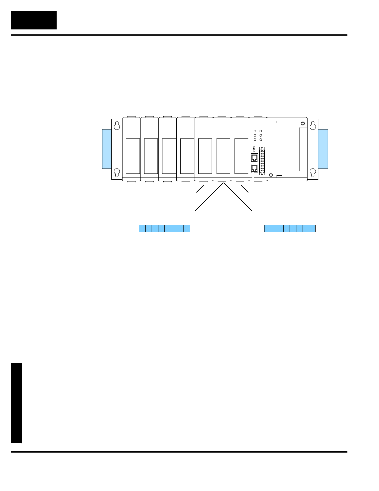
16-ChannelAnalogInput
5--14
F3--16AD 16-Channel Analog Input
F3--16A
D
Writing the Control Program
Identifying the
Data Locations
Since all channels are multiplexed into a single data word, the control program must
be setup to determine which channel is being read. Since the module provides input
points to the CPU, it is very easy to use the active channel status bits to determine
which channel is being monitored.
8pt
Relay
050
057
8pt
Output
--
Output
040
--
047
R 002, R012 R 000, R010
R 011
MSB LSB
1
1
7
8pt
030
--
037
16pt
Input
020
027
-120
127
(Analog)
16ch
010
017
-110
117
16pt
Input
000
007
100
107
--
R 001
MSB LSB
1
1
0
0
1
7
0
1
0
Page 90
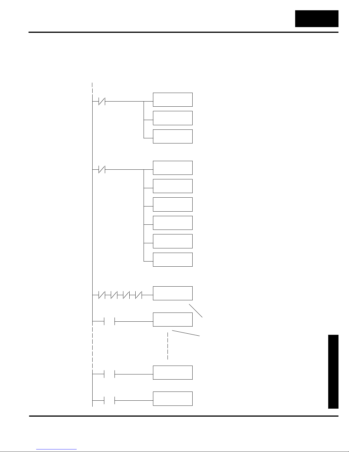
F
3
-
-
1
6
A
D
1
6
-
C
hanne
l
A
n
alo
gInpu
t
5--15
F3--16AD 16-Channel Analog Input
Example Program
The following example shows a program designed to read any of the available
channels of analog data into Register locations. Once the data is in a Register, you
can perform math on the data, compare the data against preset values, etc. Since
the DL305 CPUs use 8-bit word instructions, you have to move the data in pieces. It’s
pretty simple if you follow the example.
Read the channel ID
374
Read the data
374
DSTR2
R011
BCD F86
DOUT
R600
DSTR3
R011
DOUT1
R501
DSTR1
R001
F52
F60
F53
F61
F51
This rung loads the channel ID bits into the
accumulator from Register 011 on every scan.
Convert the channel ID status to BCD. (We’ll use
relational contacts later to make the chanel
selection much easier.)
Store the channel ID in R600. (Note, you don’t
absolutely have to do it this way. If you use R600,
then you can’t use Timer/Counter 600. You could
just use the channel indicators. See the Store
Channel 1 example that follows.)
This rung loads the four most significant data bits into
the accumulator from Register 011 on every scan.
Temporarily store the bits to Register 501.
This rung loads the eight least significant data bits
into the accumulator from Register 001.
Store channel 1
114
115 117
116
Store channel 2
CT600
K0001
=
Store channel 15
CT600=K0014
DOUT1
R500
DSTR
R500
BCD F86
DOUT
R400
DOUT
R402
DOUT
R434
F61
F50
F60
F60
F60
Temporarily store the bits to Register 500. Since
the most significant bits were loaded into 501, now
R500 and R501 contain all twelve bits in order.
Now that all the bits are stored, load all twelve bits
into the accumulator.
Math operations are performed in BCD. This
instruction converts the binary data to BCD. (You
can omit this step if your application does not
require the conversion.)
The channel selection inputs are used to let the
CPU know which channel has been loaded into the
accumulator. By using these inputs to control a
DOUT instruction, you can easily move the data to
a storage register. Notice the DOUT instruction
stores the data in two bytes. (Two bytes are
required for four digit BCD numbers.)
This rung shows how you would use the channel
indicator inputs as contacts to control the channel
selection.
This rung shows an easier way. Earlier we loaded
the channel ID bits (in BCD format) into R600. Now
we can use one relational contact to examine this
value. However, this method uses the register
associated with Timer/Counter 600. If you use this
method, make sure you don’t use the
Timer/Counter associated with the register
elsewhere in the program.
Store channel 16
CT600=K0015
DOUT
R436
F60
Page 91
16-ChannelAnalogInput
5--16
F3--16AD 16-Channel Analog Input
DL350 with a
Conventional
DL305 Base
The example below shows how to read multiple channels on an F3--08AD Analog
module in the 20--27/120--127 address slot. This module must be placed in a 16 bit
slot in order to work.
Load the data
_On
SP1
LDFK8X120
SHFL
ORFK8X20
ANDD
BCD
OUT
K8
Kfff
V2200
This rung loads the upper byte of analog data from
the module.
SHFL K8 shifts the data to the left eight places to
make room for the lower byte of data.
The ORF X20 brings the lower byte of data from
the module into the accumulator. At this time there
is a full word of data from the analog module in the
accumulator.
The ANDD Kfff masks off the twelve least
significant bits of data from the word. This is the
actual analog value.
The BCD command converts the data to BCD
format.
Stores the data in V2200.
Channel 1 Select Bit States
X125X124 X126 X127
Channel 2 Select Bit States
X125X124 X126 X127
Channel 3 Select Bit States
X125X124 X126 X127
LD
OUT
LD
OUT
LD
OUT
V2200
V3000
V2200
V3001
V2200
V3002
This sends channel one analog data to
V3000 when bits X124, X125, X126
and X127 are as shown.
This sends channel two analog data to
V3000 when bits X124, X125, X126
and X127 are as shown.
This sends channel two analog data to
V3000 when bits X124, X125, X126
and X127 are as shown.
Page 92
F
3
-
-
1
6
A
D
1
6
-
C
hanne
l
A
n
alo
gInpu
t
5--17
F3--16AD 16-Channel Analog Input
DL350 with a
D3--XX--1 Base
The example below shows how to read multiple channels on an F3--16AD Analog
module in the X0 address of the D3--XX--1 base.
_On
SP1
_On
SP1
LD VX0
SHFR
OUT
LDF X0
BCD
OUT
K12
V1400
K12
V1401
This rung loads the upper byte of analog data from
the module.
SHFL K12 shifts the word to the right twelve
places.
Puts the four channel select bits in the lower nibble
(four bits) of word V1400. This will increment once
with each scan from 0 to F.
This rung loads the twelve bits of analog data to
the module and converts it to BCD. It is the OUT to
V1401.
This convertsthe data to BCD.
The analog data (in BCD format) is then stored in
the Holding Register, V1401.
Rungs 3--18 compare the count of the chennel select bits. When the corresponding bits are true, the
channel data for that channel is stored in the proper V-memory location. For sixteen channels of
analog data, the module will require sixteen scans in order to update all channels.
Channel Selection Data
V1400
=
Channel Selection Data
V1400
=
Channel Selection Data
V1400
=
K0
K1
K2
LD
OUT
LD
OUT
LD
OUT
V1401
V2000
V1401
V2001
V1401
V2002
Channel #1 Data
Channel #2 Data
Channel #3 Data
Page 93
16-ChannelAnalogInput
5--18
F3--16AD 16-Channel Analog Input
Channel Selection Data
V1400
=
Channel Selection Data
V1400
=
Channel Selection Data
V1400
=
K3
K4
K5
LD
OUT
LD
OUT
LD
OUT
V1401
V2003
V1401
V2004
V1401
V2005
Channel #4 Data
Channel #5 Data
Channel #6 Data
Channel Selection Data
V1400
=
Channel Selection Data
V1400
=
Channel Selection Data
V1400
=
Channel Selection Data
V1400
=
K6
K7
K8
K9
LD
OUT
LD
OUT
LD
OUT
LD
V1401
V2006
V1401
V2007
V1401
V2010
V1401
Channel #7 Data
Channel #8 Data
Channel #9 Data
Channel #10 Data
OUT
V2011
Page 94
F
3
-
-
1
6
A
D
1
6
-
C
hanne
l
A
n
alo
gInpu
t
5--19
Channel Selection Data
V1400
=
Channel Selection Data
V1400
=
Channel Selection Data
V1400
=
Ka
Kb
Kc
LD
OUT
LD
OUT
LD
OUT
F3--16AD 16-Channel Analog Input
V1401
Channel #11 Data
V2012
V1401
Channel #12 Data
V2013
V1401
Channel #13 Data
V2014
Channel Selection Data
V1400
=
Channel Selection Data
V1400
=
Channel Selection Data
V1400
=
Kd
Ke
Kf
LD
OUT
LD
OUT
LD
OUT
V1401
Channel #14 Data
V2015
V1401
Channel #15 Data
V2016
V1401
Channel #16 Data
V2017
Page 95
16-ChannelAnalogInput
5--20
F3--16AD 16-Channel Analog Input
Thefollowingexampleshowshowyo
u
Scaling the Input
Data
Most applications usually require
measurements in engineering units,
which provide more meaningful data.
This is accomplished by using the
conversion formula shown.
would use the analog data to represent
pressure (PSI) from 0 to 100. This
example assumes the analog value is
1760. This should yield approximately
42.9 PSI.
Units =
Units = value in Engineering Units
A = Analog value (0 -- 4095)
S = high limit of the Engineering
unit range
A
S
4096
Units =
Units =
Units = 42.9
4096
1760
4096
A
S
100
Page 96
F
3
-
-
1
6
A
D
1
6
-
C
hanne
l
A
n
alo
gInpu
t
5--21
F3--16AD 16-Channel Analog Input
The following instructions are required to scale the data. (We’ll continue to use the
42.9 PSI example.) In this example we’re using channel 1. The active channel
indicator inputs are all off when channel 1 data is being read. Of course, if you were
using a different channel, you would use the active channel indicator point
combination that corresponds to the channel you were using.
This example assumes you have already read the analog data
and stored the BCD equivalent in R400 and R401
Scale the data
114 115 117116
DSTR
R400
F50
This instruction brings the analog value (in BCD)
into the accumulator.
Accumulator
1 7 6 0
Aux. Accumulator
0 0 0 0
R577 R576
DIV
K4096
DSTR
R576
MUL
K100
DSTR
R576
DOUT
R450
F74
F50
F73
F50
F60
The analog value is divided by the resolution of the
module, which is 4096. (1760 / 4096 = 0.4296)
Accumulator
0 0 0 0
This instruction moves the two-byte decimal
portion into the accumulator for further operations.
Accumulator
4 2 9 6
The accumulator is then multiplied by the scaling
factor, which is 100. (100 x 4296 = 429600). Notice
the most significant digits are now stored in the
auxilliary accumulator. (This is different from the
way the Divide instruction operates.)
Accumulator
9 6 0 0
This instruction moves the two-byte auxilliary
accumulator for further operations.
Accumulator
0 0 4 2
Aux. Accumulator
4 2 9 6
R577 R576
Aux. Accumulator
4 2 9 6
R577 R576
Aux. Accumulator
0 0 4 2
R577 R576
Aux. Accumulator
0 0 4 2
R577 R576
This instruction stores the accumulator to R450.
R450 now contains the PSI, which is 42 PSI.
Accumulator
0 0 4 2
Store in R451 & R450
0 0 4 2
R451 R450
Page 97
16-ChannelAnalogInput
5--22
F3--16AD 16-Channel Analog Input
You probably noticed the previous example yielded 42 PSI when the real value
should have been 42.9 PSI. By changingthe scalingvalue slightly, we can “imply” an
extra decimal of precision. Notice in the following example we’ve added another digit
to the scale. Instead of a scale of 100, we’re using 1000, which implies 100.0 for the
PSI range.
This example assumes you have already read the analog data
and stored the BCD equivalent in R400 and R401
Scale the data
114 115 117116
DSTR
R400
F50
This instruction brings the analog value (in BCD)
into the accumulator.
Accumulator
1 7 6 0
Aux. Accumulator
0 0 0 0
R577 R576
DIV
K4096
DSTR
R576
MUL
K1000
DSTR
R576
DOUT
R450
F74
F50
F73
F50
F60
The analog value is divided by the resolution of the
module, which is 4096. (1760 / 4096 = 0.4296)
Accumulator
0 0 0 0
This instruction moves the two-byte decimal
portion into the accumulator for further operations.
Accumulator
4 2 9 6
The accumulator is multiplied by the scaling factor,
which is now 1000. (1000 x 4296 = 4296000). The
most significant digits are now stored in the
auxilliary accumulator. (This is different from the
way the Divide instruction operates.)
Accumulator
6 0 0 0
This instruction moves the two-byte auxilliary
accumulator for further operations.
Accumulator
0 4 2 9
This instruction stores the accumulator to R450
and R451. R450 and R451 now contain the PSI,
which implies 42.9.
Accumulator
0 4 2 9
Aux. Accumulator
4 2 9 6
R577 R576
Aux. Accumulator
4 2 9 6
R577 R576
Aux. Accumulator
0 4 2 9
R577 R576
Aux. Accumulator
0 4 2 9
R577 R576
Store in R451 & R450
0 4 2 9
R451 R450
Page 98

F
3
-
-
1
6
A
D
1
6
-
C
hanne
l
A
n
alo
gInpu
t
5--23
F3--16AD 16-Channel Analog Input
This example program shows how you can use the instructions to load these
equation constants into data registers. The example is written for channel 1, but you
can easily use a similar approach to use different scales for all channels if required.
You may just use the appropriate constants in the instructions dedicated for each
channel, but this method allows easier modifications. For example, you could easily
use an operator interface or a programming device to change the constants if they
are stored in Registers.
Load the constants
374
DSTR
K4096
F50
On the first scan, these first two instructions load
the analog resolution (constant of 4096) into R460
and R461.
Read the data
374
Store channel 1
114 115 117116
DOUT
R460
DSTR
K1000
DOUT
R462
DSTR3
R011
DOUT1
R501
DIV
R460
DSTR
R576
MUL
R462
F60
F50
F60
F53
F61
F74
F50
F73
These two instructions load the high limit of the
Engineering unit scale (constant of 1000) into
R462 and R463. Note, if you have different scales
for each channel, you’ll also have to enter the
Engineering unit high limit for those as well.
This rung loads the four most significant data bits into
the accumulator from Register 011 on every scan.
Temporarily store the bits to Register 501.
The analog value is divided by the resolution of the
module, which is stored in R460.
This instruction moves the decimal portion from the
auxilliary accumulator into the regular accumulator
for further operations.
The accumulator is multiplied by the scaling factor,
which is stored in R462.
DSTR
R576
DOUT
R400
F50
F60
This instruction moves most significant digits (now
stored in the auxilliary accumulator) into the
regular accumulator for further operations.
The scaled value is stored in R400 and R401 for
further use.
Page 99
16-ChannelAnalogInput
5--24
F3--16AD 16-Channel Analog Input
Scaling on a DL350
with a
Conventional
DL305 Base
The example below shows how to scale input data from an F3--04ADS Analog
module in the 20--27/120--127 address slot. This module must be placed in a 16 bit
slot in order to work.
Load the data
_On
SP1
LDFK8X120
SHFL K8
ORF
ANDD Kfff
BCD
OUT V2200
X20
K8
This loads the upper byte of the analog data from
the module.
SHFL K8 shifts the data to the left eight places to
make room for the lower byte of data.
The ORF X20 brings the lower byte of data from
the module into the accumulator. At this time there
is a full word of data from the analog module in the
accumulator.
The ANDD Kfff masks off the twelve least
significant bits of data from the word. This is the
actual analog value.
The BCD command converts the data to BCD
format.
The scaled value is stored in V3010 with an
implied decimal.
Channel 1 Select Bit States
X125X124 X126 X127
Scale the data
_On
SP1
LD
OUT
LD
Channel 2
Analog Data
Register (BCD)
V3000
MUL K2000
DIV K4096
OUT V3010
This writes channel one analog data to
V2200
V3000
Rung 3 scales a 0 to 200 range of a transducer
over the 4096 counts. The raw analog value is
loaded to the accumulator from V3001
(Channel #1).
It is then multiplied by 2000. The additional zero
provides a higher degree of resolution.
It is then divided by 4096, which is the resolution of
the module.
The scaled value is stored in V3010 with an
implied decimal.
V3000 when bits X124, X125, X126
and X127 are as shown.
Page 100
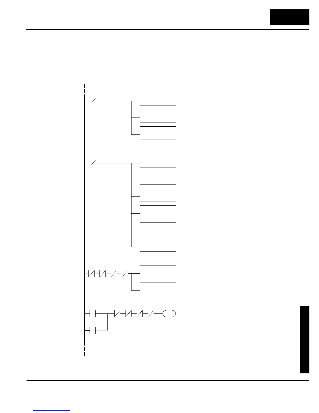
F
3
-
-
1
6
A
D
1
6
-
C
hanne
l
A
n
alo
gInpu
t
5--25
F3--16AD 16-Channel Analog Input
Broken Transmitter
Detection
If you use 4--20mA signals you can easily check for broken transmitter conditions.
Since you have to use the 0--20mA range and the lowest signal for the 4--20mA
transmitter is 4mA, the lowest digital value for the signal is not 0, but instead is 819.
If the transmitter is workingproperly thesmallest valueyou should ever see is 819. If
you see a value of less than about 750 (allowing for tolerance), then you know the
transmitter is broken.
Read the channel ID
374
Read the data
374
DSTR2
R011
BCD F86
DOUT
R600
DSTR3
R011
DOUT1
R501
DSTR1
R001
F52
F60
F53
F61
F51
This rung loads the channel ID bits into the
accumulator from Register 011 on every scan.
Convert the channel ID status to BCD. We’ll use
relational contacts later to make the chanel
selection much easier.)
Store the channel ID in R600.
This rung loads the four most significant data bits into
the accumulator from Register 011 on every scan.
Temporarily store the bits to Register 501.
This rung loads the eight least significant data bits
into the accumulator from Register 001.
DOUT1
R500
DSTR
R500
BCD F86
Store channel 1
114 115 117116
Broken transmitter indicator on channel 1
773
774
114 115 117116
DOUT
R400
CMP
K0100
F61
F50
F60
F70
040
OUT
Temporarily store the bits to Register 500. Since
the most significant bits were loaded into 501, now
R500 and R501 contain all twelve bits in order.
Now that all the bits are stored, load all twelve bits
into the accumulator.
Math operations are performed in BCD. This
instruction converts the binary data to BCD. (You
can omit this step if your application does not
require the conversion.)
The DOUT instruction copies the accumulator data
to R400 and R401. Since the data is still in the
accumulator, we can compare it against a
constant. Since the minimum value for a 4mA
signal is 819 (minus the module tolerance), we can
choose a value for the compare. We picked 100,
but you could choose something else from 0 to
about 750.
Flags 773 and 774 are used with the Compare
instruction. In this example if the analog value is
less than or equal to 100, then output 040 is turned
on.
You may want to latch 040 to catch intermittent
broken transmitters.
 Loading...