

AUSTN AS8E128K32Q-15-XT, AS8E128K32Q-15-IT Datasheet
EEPROM
AS8ER128K32
Austin Semiconductor, Inc.
AS8ER128K32
Rev. 3.0 1/02
Austin Semiconductor, Inc. reserves the right to change products or specifications without notice.
1
GENERAL DESCRIPTION
The Austin Semiconductor, Inc. AS8ER128K32 is a 4 Megabit
Radiation Tolerant EEPROM Module organized as 128K x 32 bit.
User configurable to 256K x16 or 512Kx 8. The module achieves high
speed access, low power consumption and high reliability by employing advanced CMOS memory technology.
The military grade product is manufactured in compliance to
MIL-STD 883, making the AS8ER128K32 ideally suited for military
or space applications.
The module is offered as a 68 lead 0.990 inch square ceramic
quad flat pack. It has a max. height of 0.200 inch. This package design
is targeted for those applications which require low profile SMT Packaging.
* contact factory for test reports. ASI does not guarantee or warrant these
performance levels, but references these third party reports.
FEATURES
• Access time of 150ns
• Operation with single 5V + 10% supply
• Power Dissipation:
Active: 1.43 W (MAX), Max Speed Operation
Standby: 7.7 mW (MAX), Battery Back-up Mode
• On-Chip Latches: Address, Data, CE\, OE\, WE\
• Automatic Byte Write: 10 ms (MAX)
• Automatic Page Write (128 bytes): 10 ms (MAX)
• Data protection circuit on power on/off
• Low power CMOS
•104 Erase/Write cycles (in Page Mode)
• Software data protection
• TTL Compatible Inputs and Outputs
• Data Retention: 10 years
• Ready/Busy\ and Data Polling Signals
• Write protection by RES\ pin
• Radiation Tolerant: Proven total dose 40K to 100K RADS*
• Operating Temperature Ranges:
Military: -55oC to +125oC
Industrial: -40oC to +85oC
OPTIONS MARKINGS
• Timing
150 ns -1 5
• Package
Ceramic Quad Flat pack Q No. 703
AVAILABLE AS MILITARY
SPECIFICATIONS
• MIL-STD-883
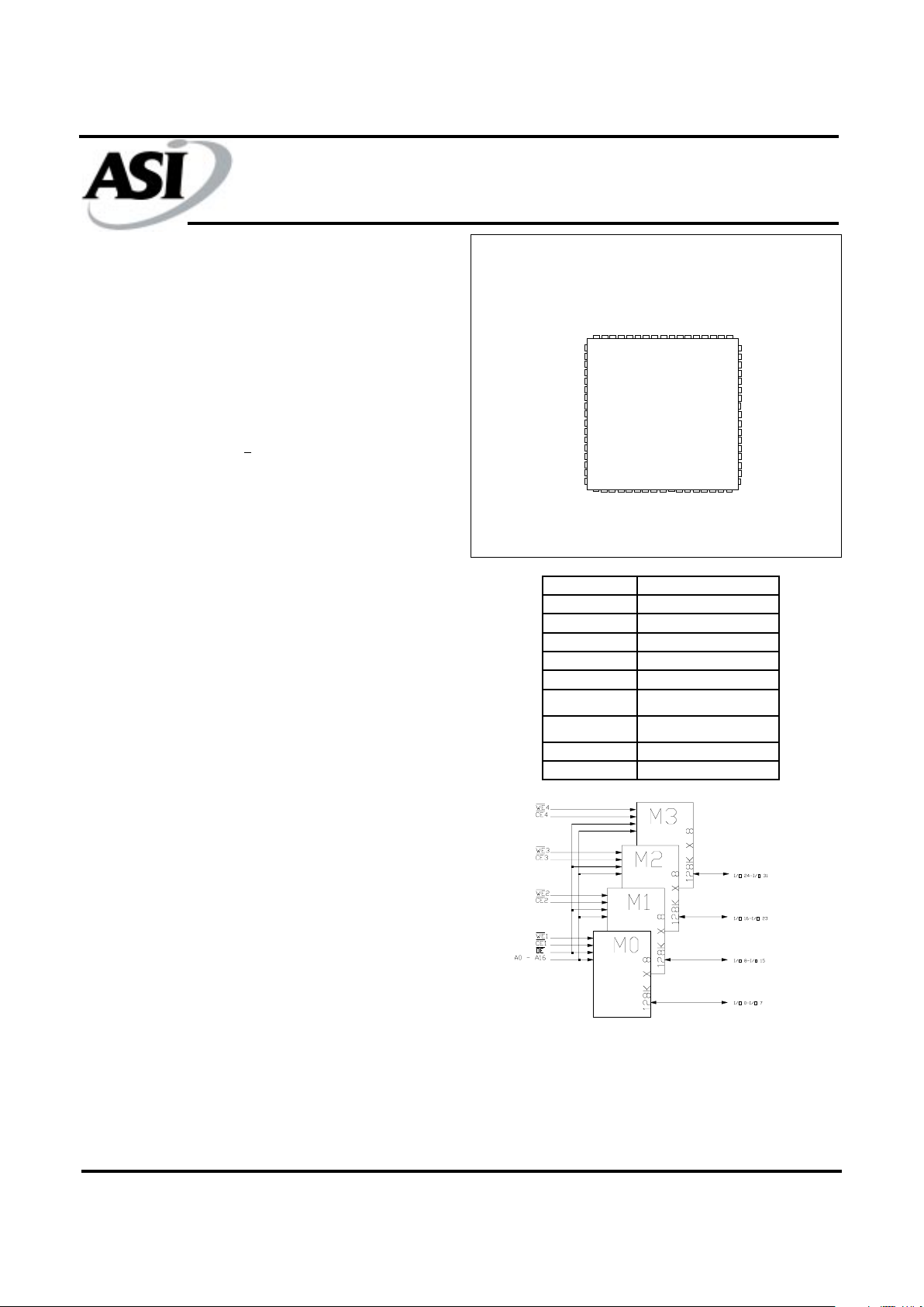
PIN ASSIGNMENT
(T op Vie w)
68 Lead CQFP
128K x 32 EEPROM
Radiation Tolerant
EEPROM Memory Array
For more products and information
please visit our web site at
www.austinsemiconductor .com
I/O0
I/O1
I/O2
I/O3
I/O4
I/O5
I/O6
I/O7
GND
I/O8
I/O9
I/O10
I/O11
I/O12
I/O13
I/O14
I/O15
9 8 7 6 5 4 3 2 1 68 67 66 65 64 63 62 61
RES\A0A1A2A3A4A5
CS3\
GND
CS4\
WE1\A6A7A8A9
A10
Vcc
27 28 29 30 31 32 33 34 35 36 37 38 39 40 41 42 43
Vcc
A11
A12
A13
*A15
*A14
A16
CS1\
OE\
CS2\
NC
WE2\
WE3\
WE4\
NC
NC
RDY
10
11
12
13
14
15
16
17
18
19
20
21
22
23
24
25
26
60
59
58
57
56
55
54
53
52
51
50
49
48
47
46
45
44
I/O16
I/O17
I/O18
I/O19
I/O20
I/O21
I/O22
I/O23
GND
I/O24
I/O25
I/O26
I/O27
I/O28
I/O29
I/O30
I/O31
PIN NAME
FUNCTION
A0 to A16 Address Input
I/O0 to I/O31 Data Input/Output
OE\ Output Enable
CE\ Chip Enable
WE\ Write Enable
V
CC
Power Supply
V
SS
Ground
RDY/BUSY\ Ready Busy
RES\ Reset
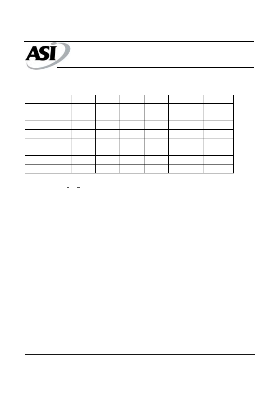
FUNCTIONAL BLOCK DIAGRAM
*Pin #'s 31 and 32, A15 and A14 respectively, are reversed from the AS8E128K32. Correct
use of these address lines is required for operation of the SDP mode to work properly.
EEPROM
AS8ER128K32
Austin Semiconductor, Inc.
AS8ER128K32
Rev. 3.0 1/02
Austin Semiconductor, Inc. reserves the right to change products or specifications without notice.
2
NOTES: 1. RDY/Busy\ output has only active LOW VOL and high impedance state. It can not go to HIGH (VOH) state.
2. VCC -0.5 < VH < VCC +1.0
3. X : DON'T CARE
TRUTH T ABLE
MODE CE\ OE\ WE\ RES\
RDY/BUSY\
1
I/O
Read
V
IL
V
IL
V
IH
V
H
2
High-Z Dout
Standby
V
IH
X
3
X X High-Z High-Z
Write
V
IL
V
IH
V
IL
V
H
High-Z to V
OL
Din
Deselect
V
IL
V
IH
V
IH
V
H
High-Z High-Z
XX
V
IH
X --- ---
X
V
IL
X X --- ---
Data\ Polling
V
IL
V
IL
V
IH
V
H
V
OL
Dout (I/O7)
Program Reset X X X
V
IL
High-Z High-Z
Wirte Inhibit
EEPROM
AS8ER128K32
Austin Semiconductor, Inc.
AS8ER128K32
Rev. 3.0 1/02
Austin Semiconductor, Inc. reserves the right to change products or specifications without notice.
3
*Stresses greater than those listed under "Absolute Maximum
Ratings" may cause permanent damage to the device. This is
a stress rating only and functional operation of the device at
these or any other conditions above those indicated in the
operation section of this specification is not implied. Exposure
to absolute maximum rating conditions for extended periods
may affect reliability .
**Junction temperature depends upon package type, cycle time,
loading, ambient temperature and airflow, and humidity
(plastics).
ABSOLUTE MAXIMUM RATINGS*
Voltage on Vcc Supply Relative to Vss
Vcc ....................................................................-0.6V to +7.0V
Operating Temperature Range
(1)
..................-55°C to +125°C
Storage Temperature Range .........................-65°C to +150°C
Voltage on any Pin Relative to Vss..............-0.5V to +7.0V
(2)
Max Junction T emperature**.......................................+150°C
Thermal Resistance junction to case (θ
JC
):
Package T ype Q...........................................11.3° C/W
Package T ype P & PN..................................2.8° C/W
NOTES:
1) Including electrical characteristics and data retention.
2) VIN MIN = -3.0V for pulse width < 20ns.
ELECTRICAL CHARACTERISTICS AND RECOMMENDED DC OPERATING CONDITIONS
(-55oC<TA<125oC or -40oC to +85oC; Vcc = 5V + 10%)
MAX
CONDITIONS SYM -15 UNITS
Iout = 0mA, V
CC
= 5.5V
Cycle = 1µS, Duty = 100%
80
Iout = 0mA, V
CC
= 5.5V
Cycle = MIN, Duty = 100%
260
CE\ = V
CC,
VCC = 5.5V I
CC1
1.4 mA
CE\ = V
IH,
VCC = 5.5V I
CC2
12 mA
Power Supply Current:
Standby
I
cc3
mA
PARAMETER
Power Supply Current:
Operating
PARAMETER CONDITIONS SYMBOL MIN MAX UNITS
Input High Voltage
V
IH
2.2
V
CC
+0.3
V
Input High Voltage (RES\)
V
H
VCC -0.5 VCC +1.0
V
Input Low Voltage
V
IL
-0.3
1
0.8 V
INPUT LEAKAGE CURRENT
OV <
VIN < V
CC
I
LI
-10 10
µΑ
OUTPUT LEAKAGE CURRENT
Outputs(s) Disabled,
OV <
V
OUT
< V
CC
I
LO
-10 10
µΑ
Output High Voltage
I
OH
= -0.4mA V
OH
2.4 -- V
Output Low Voltage
I
OL
= 2.1mA V
OL
-- 0.4 V
Supply Voltage
V
CC
4.5 5.5 V
2
NOTE: 1) V
IL
(MIN): -1.0V for pulse width < 20ns.
2) ILI on RES\ : 500µA (MAX)
EEPROM
AS8ER128K32
Austin Semiconductor, Inc.
AS8ER128K32
Rev. 3.0 1/02
Austin Semiconductor, Inc. reserves the right to change products or specifications without notice.
4
NOTE: 1. This parameter is guaranteed but not tested.
CAP ACIT ANCE T ABLE
1
(V
IN
= 0V, f = 1 MHz, TA = 25oC)
SYMBOL PARAMETER MAX UNITS
C
ADD
A0 - A16 Capacitance 40 pF
C
OE
OE\, RES\, RDY Capacitance 40 pF
C
WE, CCE
WE\ and CE\ Capacitance 12 pF
C
IO
I/O 0- I/O 31 Capacitance 20 pF
ELECTRICAL CHARACTERISTICS AND RECOMMENDED AC OPERATING CONDITIONS
(-55oC < TA < +125oC or -40oC to +85oC; Vcc = 5V +10%)
MIN MAX
Address to Output Delay
CE\ = OE\ = V
IL
, WE\ = V
IH
t
ACC
150 ns
CE\ to Output Delay
OE\ = V
IL
, WE\ = V
IH
t
CE
150 ns
OE\ to Output Delay OE\ = V
IL
, WE\ = V
IH
t
OE
10 75 ns
Address to Output Hold CE\ = OE\ = V
IL
, WE\ = V
IH
t
OH
0ns
CE\ or OE\ high to Output Float (1)
OE\ = V
IL
, WE\ = V
IH
t
DF
050ns
RES\ low to Output Float (1) CE\ = OE\ = V
IL
, WE\ = V
IH
t
DFR
0 350 ns
RES\ to Output Delay CE\ = OE\ = V
IL
, WE\ = V
IH
t
RR
0 450 ns
DESCRIPTION
150
SYMBOL UNITS
TEST CONDITIONS
AC TEST CHARACTERISTICS
TEST SPECIFICA TIONS
Input pulse levels...........................................VSS to 3V
Input rise and fall times...........................................5ns
Input timing reference levels.................................1.5V
Output reference levels.........................................1.5V
Output load................................................See Figure 1
OH
OL
I
I
Current Source
Current Source
Vz = 1.5V
(Bipolar
Supply)
Device
Under
Test
Ceff = 50pf
-+
+
NOTES:
Vz is programmable from -2V to + 7V.
IOL and IOH programmable from 0 to 16 mA.
Vz is typically the midpoint of VOH and VOL.
IOL and IOH are adjusted to simulate a typical resistive load
circuit.
Figure 1

EEPROM
AS8ER128K32
Austin Semiconductor, Inc.
AS8ER128K32
Rev. 3.0 1/02
Austin Semiconductor, Inc. reserves the right to change products or specifications without notice.
5
ELECTRICAL CHARACTERISTICS AND RECOMMENDED AC WRITE CHARACTERISTICS
(-55
o
C < TA < +125oC; Vcc = 5V +10%)
SYMBOL PARAMETER MIN
(2)
MAX UNITS
t
AS
Address Setup Time 0 ms
t
AH
Address Hold Time 150 ns
t
CS
CE\ to Write Setup Time (WE\ controlled) 0 ns
t
CH
CE\ Hold Time (WE\ controlled) 0 ns
t
WS
WE\ to Write Setup Time (CE\ controlled) 0 ns
t
WH
WE\ to Hold Time (CE\ controlled) 0 ns
t
OES
OE\ to Write Setup Time 0 ns
t
OEH
OE\ to Hold Time 0 ns
t
DS
Data Setup Time 100 ns
t
DH
Data Hold Time 10 ns
t
WP
WE\ Pulse Width (WE\ controlled) 250 ns
t
CW
CE\ Pulse Width (CE\ controlled) 250 ns
t
DL
Data Latch Time 300 ns
t
BLC
Byte Load Cycle 0.55 30 µs
t
BL
Byte Load Window 100 µs
t
WC
Write Cycle Time
10
(3)
ms
t
DB
Time to Device Busy 120 ns
t
DW
Write Start Time
150
(4)
ns
t
RP
Reset Protect Time 100 µs
t
RES
Reset High Time
(5)
1µs
READ TIMING WA VEFORM
t
ACC
t
CE
t
OE
t
OH
t
DF
t
DFR
t
RR
HIGH-Z
ADDRESS
CE\
OE\
WE\
Data Out
RES\
DA T A OUT V ALID
V
IH
 Loading...