

AUSTN AS4LC4M4883C Datasheet
AUSTIN SEMICONDUCTOR, INC.
1
2
3
4
5
6
8
9
10
11
12
13
26
25
24
23
22
21
19
18
17
16
15
14
AS4LC4M4 883C
4 MEG x 4 DRAM
DRAM
4 MEG x 4 DRAM
3.3V, EDO PAGE MODE
AVAILABLE IN MILITARY
SPECIFICATIONS
• MIL-STD-883
• SMD Planned
FEATURES
• Industry-standard x4 pinout, timing, functions and
packages
• High-performance CMOS silicon-gate process
• Single +3.3V ±0.3V power supply
• Low power, 1mW standby; 150mW active, typical
• All inputs, outputs and clocks are TTL-compatible
• Refresh modes: ?R?A/S ONLY, ?C?A/S-BEFORE-?R?A/S (CBR)
HIDDEN
• 2,048-cycle (11 row-, 11 column-addresses)
• Extended Data-Out (EDO) PAGE access cycle
• 5V-tolerant I/Os (5.5V maximum V
IH level)
OPTIONS MARKING
• Timing
60ns access (Contact Factory) -6
70ns acess -7
80ns access -8
• Packages
Ceramic SOJ ECJ No. 505
Ceramic LCC EC No. 212
Ceramic Gull Wing ECG No. 603
KEY TIMING PARAMETERS
SPEEDtRCtRACtPC
-6 110ns 60ns 30ns 30ns 15ns 12ns
-7 130ns 70ns 35ns 35ns 18ns 15ns
-8 150ns 80ns 40ns 40ns 20ns 20ns
t
AAtCACtCAS
GENERAL DESCRIPTION
The AS4LC4M4 is a randomly accessed solid-state
memory containing 16,777,216 bits organized in a x4 configuration. The AS4LC4M4 ?R?A/S is used to latch the first 11
bits and ?C?A/S the latter 11 bits. READ and WRITE cycles are
selected with the ?W/E input. A logic HIGH on
?W/E dictates READ mode while a logic LOW on ?W/E dictates
WRITE mode. During a WRITE cycle, data-in (D) is latched
by the falling edge of ?W/ E or ?C?A/S, whichever occurs last. If
?W/E goes LOW prior to ?C?A/S going LOW, the output pins
remain open (High- Z) until the next ?C?A/S cycle, regardless
of ?O/E.
AS4LC4M4 Austin Semiconductor, Inc., reserves the right to change products or specifications without notice.
Rev. 11/97
DS000022
LOW on ?W/E dictates WRITE mode. During a WRITE cycle,
data-in (D) is latched by the falling edge of ?W/E or /C/A/S,
whichever occurs last. An EARLY WRITE occurs when
?W/E is taken LOW prior to /C/A/S falling. A LATE WRITE or
READ-MODIFY-WRITE occurs when ?W/E falls after /C/A/S
was taken LOW. During EARLY WRITE cycles, the dataoutputs (Q) will remain High-Z regardless of the state of
?O/E. During LATE WRITE or READ-MODIFY-WRITE cycles,
?O/E must be taken HIGH to disable the data-outputs prior to
applying input data. If a LATE WRITE or READ-MODIFYWRITE is attempted while keeping ?O/E LOW, no write will
occur, and the data-outputs will drive read data from the
accessed location.
through four pins using common I/O, and pin direction is
controlled by ?W/E and ?O/E.
FAST PAGE MODE
(READ, WRITE or READ-MODIFY-WRITE) within a rowaddress-defined page boundary. The FAST PAGE cycle is
always initiated with a row-address strobed-in by ?R?A/S
followed by a column-address strobed-in by ?C?A/S. ?C?A/S may
be toggled-in by holding ?R?A/S LOW and strobing-in different column-addresses, thus executing faster memory cycles.
Returning R?A/S HIGH terminates the FAST PAGE MODE
of operation.
2-73
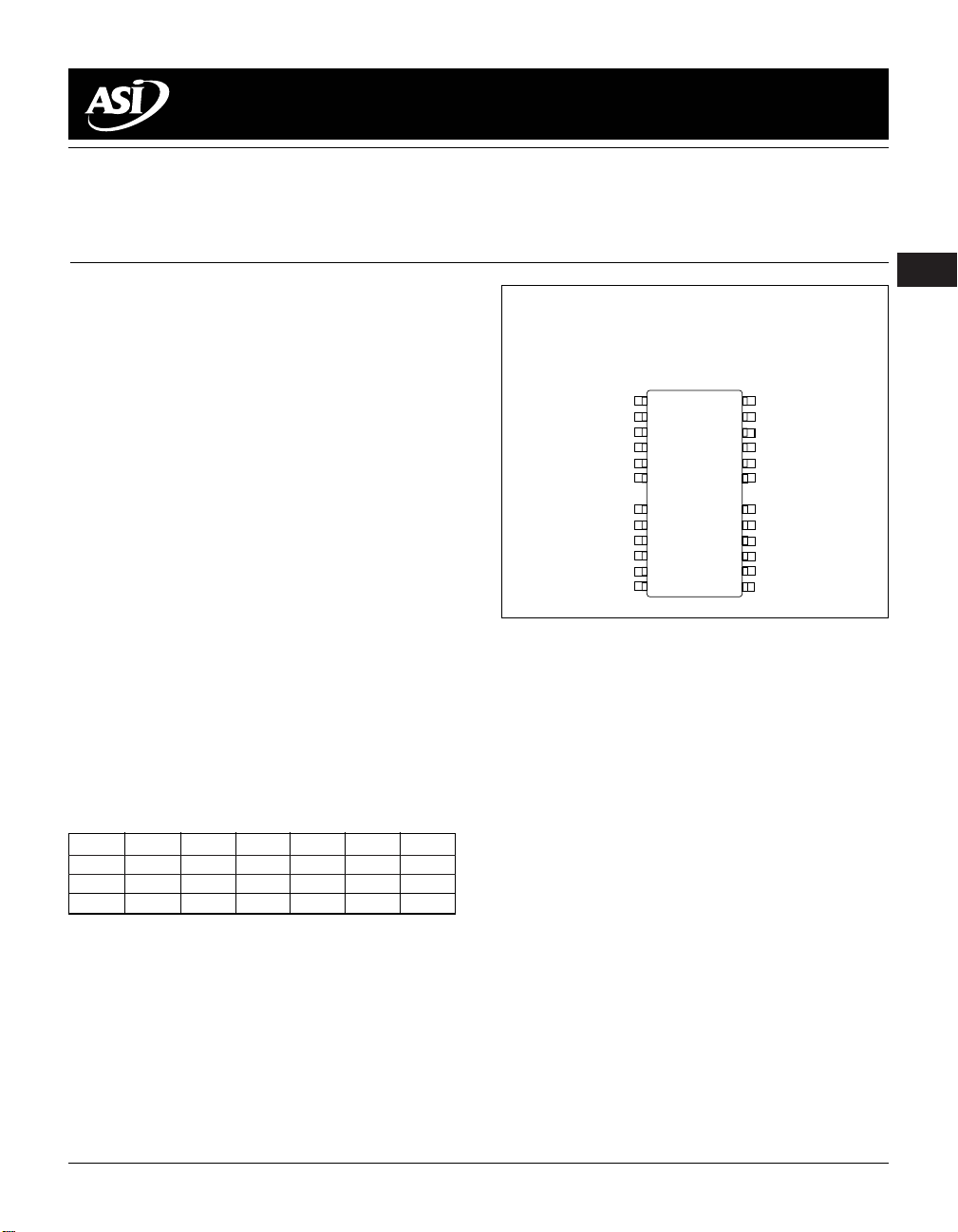
PIN ASSIGNMENT (Top View)
24/28-Pin
28
1
VCC
2
DQ1
3
DQ2
4
/W/E
5
/R/A/S
6
NC
9
A10
10
A0
11
A1
12
A2
13
A3
14
V
CC
A logic HIGH on ?W/E dictates READ mode while a logic
The four data inputs and the four data outputs are routed
FAST PAGE operations allow faster data operations
VSS
27
DQ4
26
DQ3
25
/C/A/S
24
/O/E
23
A9
20
A8
19
A7
18
A6
17
A5
16
A4
15
Vss
AUSTIN SEMICONDUCTOR, INC.
,
,,
,,
,,,
,,
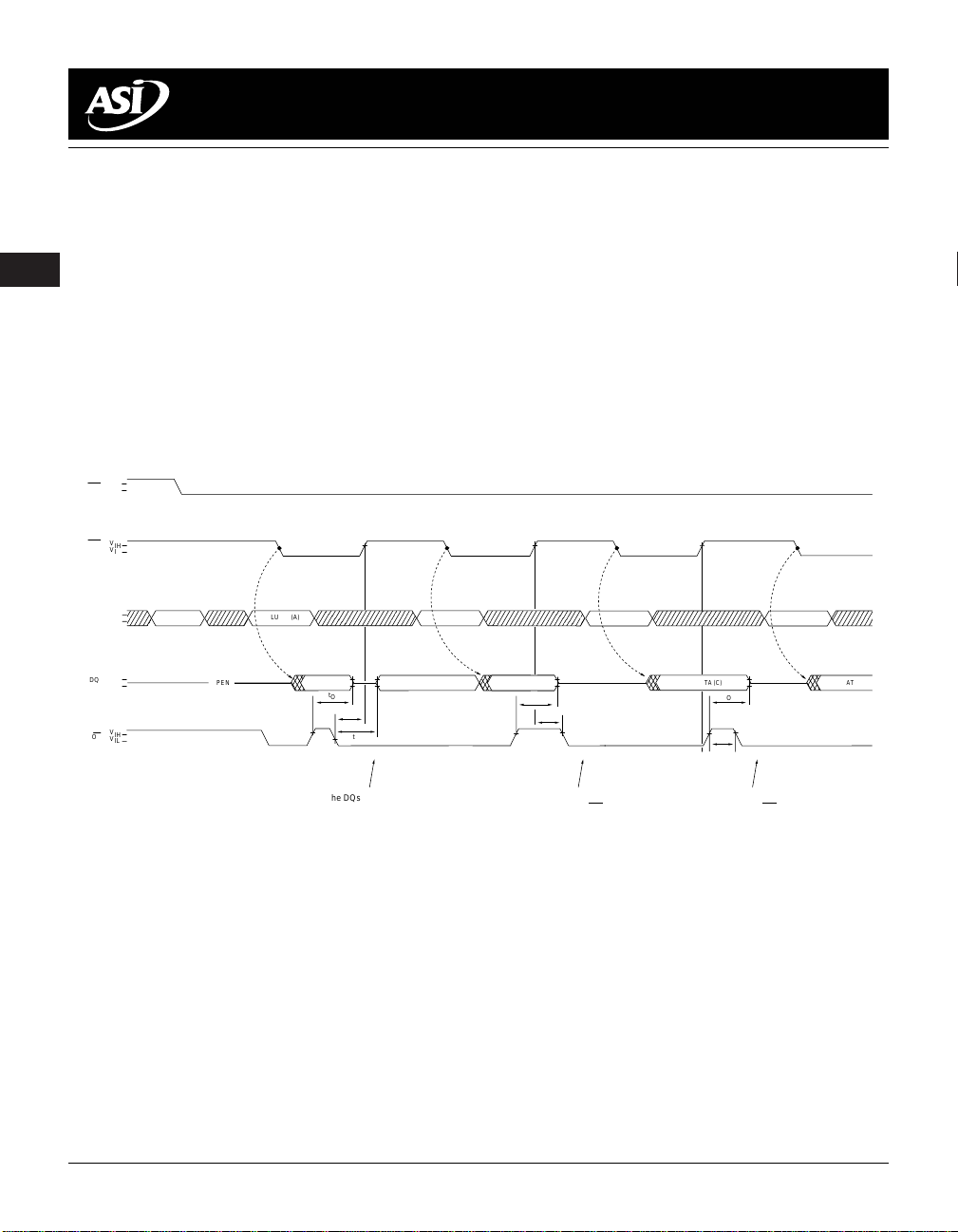
EDO PAGE MODE
The AS4LC4M4E8 provides EDO PAGE MODE which is
an accelerated FAST PAGE MODE cycle. The primary
advantage of EDO is the availability of data-out even after
?C?A/S returns HIGH. EDO allows ?C?A/S precharge time (
to occur without the output data going invalid. This elimination of ?C?A/S output control allows pipeline READs.
FAST-PAGE-MODE DRAMs have traditionally turned
the output buffers off (High-Z) with the rising edge of
?C?A/S. EDO-PAGE-MODE DRAMs operate similarly to
FAST-PAGE-MODE DRAMs, except data will remain valid
or become valid after ?C?A/S goes HIGH during READs,
provided ?R?A/S and ?O/E are held LOW. If ?O/E is pulsed while
V
IH
RAS
V
IL
V
CAS
IH
V
IL
V
IH
ADDR
V
ROW
IL
COLUMN (A)
t
CP)
COLUMN (B)
AS4LC4M4 883C
4 MEG x 4 DRAM
?R?A/S and ?C?A/S are LOW, data will toggle from valid data to
High-Z and back to the same valid data. If ?O/E is toggled or
pulsed after ?C?A/S goes HIGH while ?R?A/S remains LOW,
data will transition to and remain High-Z (refer to Figure 1).
?W/E can also perform the function of disabling the output
devices under certain conditions, as shown in Figure 2.
During an application, if the DQ outputs are wire OR’d,
?O/E must be used to disable idle banks of DRAMs. Alternatively, pulsing ?W/E to the idle banks during ?C?A/S high time
will also High-Z the outputs. Independent of ?O/E control,
the outputs will disable after
from the rising edge of ?R?A/S or ?C?A/S, whichever occurs last.
COLUMN (C)
t
OFF, which is referenced
COLUMN (D)
DQ
OE
AS4LC4M4 Austin Semiconductor, Inc., reserves the right to change products or specifications without notice.
Rev. 11/97
DS000022
V
IOH
V
IOL
V
IH
V
IL
OPEN
VALID DATA (A)
t
OD
t
OES
The DQs go back to
Low-Z if
t
OE
t
OES is met.
VALID DATA (A)
VALID DATA (B)
t
OD
t
OEHC
The DQs remain High-Z
until the next CAS cycle
t
OEHC is met.
if
VALID DATA (C)
t
OEP
The DQs remain High-Z
until the next CAS cycle
t
OEP is met.
if
t
OD
VALID DATA (D)
Figure 1
OUTPUT ENABLE AND DISABLE
2-74
AUSTIN SEMICONDUCTOR, INC.
,
,
,
,,,
AS4LC4M4 883C
4 MEG x 4 DRAM
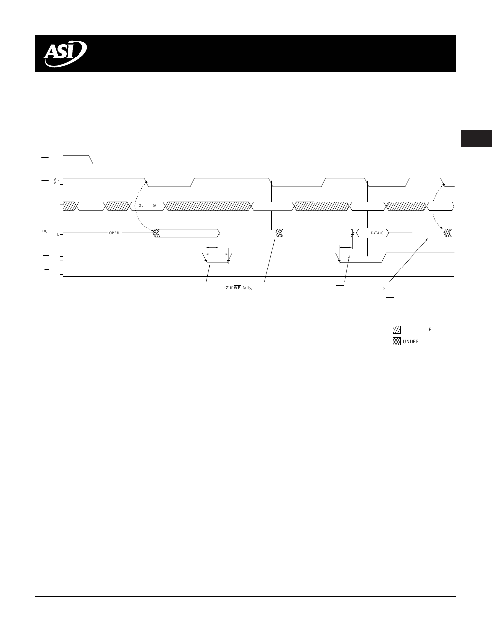
REFRESH
Preserve correct memory cell data by maintaining power and executing a ?R?A/S cycle (READ, WRITE) or ?R?A/S refresh cycle
(?R?A/S ONLY, CBR, or HIDDEN) so that all 2,048 combinations of ?R?A/S addresses are executed at least every 32ms, regardless
of sequence. The CBR REFRESH cycle will invoke the refresh counter for automatic ?R?A/S addressing.
V
IH
RAS
V
IL
V
IH
CAS
V
IL
V
ADDR
IH
V
IL
V
IOH
DQ
V
IOL
V
IH
WE
V
IL
V
IH
OE
V
IL
ROW
OPEN
COLUMN (A)
COLUMN (B)
VALID DATA (A)
t
WHZ
t
WPZ
The DQs go to High-Z if WE falls, and if tWPZ is met,
will remain High-Z until CAS goes LOW with
WE HIGH (i.e., until a READ cycle is initiated).
VALID DATA (B)
COLUMN (C)
INPUT DATA (C)
t
WHZ
WE may be used to disable the DQs to prepare
for input data in an EARLY WRITE cycle. The DQs
will remain High-Z until CAS goes LOW with
WE HIGH (i.e., until a READ cycle is initiated).
COLUMN (D)
DON’T CARE
UNDEFINED
Figure 2
??
//
?W
/E CONTROL OF DQs
??
//
AS4LC4M4 Austin Semiconductor, Inc., reserves the right to change products or specifications without notice.
Rev. 11/97
DS000022
2-75
AUSTIN SEMICONDUCTOR, INC.
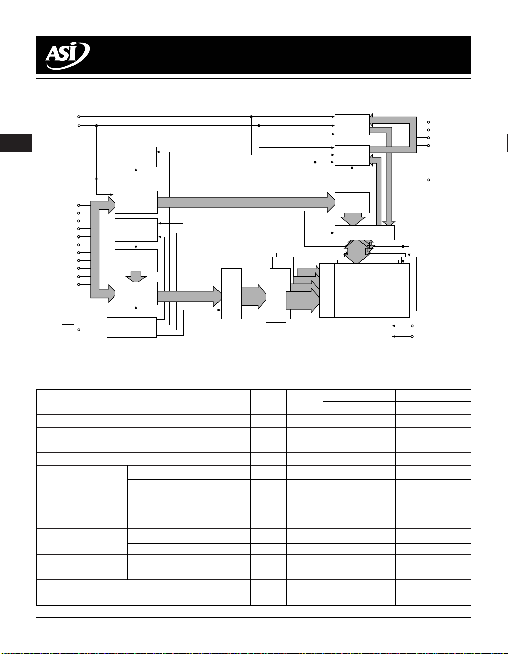
FUNCTIONAL BLOCK DIAGRAM
AS4LC4M4 883C
4 MEG x 4 DRAM
WE
CAS
A10
RAS
DATA-IN
BUFFER
NO. 2 CLOCK
GENERATOR
COLUMNADDRESS
A0
A1
A2
A3
A4
A5
A6
A7
A8
A9
11
11
BUFFER(11)
REFRESH
CONTROLLER
REFRESH
COUNTER
11
ROW-
ADDRESS
BUFFERS (11)
NO. 1 CLOCK
GENERATOR
11
10
ROW
DECODER
1
2048
2048
2048
2048
2048
SELECT
COMPLEMENT
DATA-OUT
BUFFER
COLUMN
DECODER
1024
SENSE AMPLIFIERS
I/O GATING
1024
4096 x 1024 x 4
MEMORY
(2 of 4096)
ROW SELECT
ARRAY
4
4
4
4
(1 OF 2)
(1 OF 2)
ROW TRANSFER
ROW TRANSFER
DD
V
Vss
DQ1
DQ2
DQ3
DQ4
OE
TRUTH TABLE
ADDRESSES DATA-IN/OUT
FUNCTION ?R?A/S ?C?A/S ?W/E ?O/E
t
R
Standby H H>XXXXX High-Z
READ L L H L ROW COL Data-Out
EARLY WRITE L L L X ROW COL Data-In
READ WRITE L L H>LL>H ROW COL Data-Out, Data-In
EDO-PAGE-MODE 1st Cycle L H>L H L ROW COL Data-Out
READ 2nd Cycle L H>L H L n/a COL Data-Out
EDO-PAGE-MODE 1st Cycle L H>L L X ROW COL Data-In
EARLY-WRITE 2nd Cycle L H>L L X n/a COL Data-In
Any Cycle L L>H H L n/a n/a Data-Out
EDO-PAGE-MODE 1st Cycle L H>LH>LL>H ROW COL Data-Out, Data-In
READ-WRITE 2nd Cycle L H>LH>LL>H n/a COL Data-Out, Data-In
HIDDEN READ L>H>L L H L ROW COL Data-Out
REFRESH WRITE L>H>L L L X ROW COL Data-In
?R?A/S-ONLY REFRESH L H X X ROW n/a High-Z
CBR REFRESH H>L L H X X X High-Z
t
C DQ1-DQ4
AS4LC4M4 Austin Semiconductor, Inc., reserves the right to change products or specifications without notice.
Rev. 11/97
DS000022
2-76
AUSTIN SEMICONDUCTOR, INC.
AS4LC4M4 883C
4 MEG x 4 DRAM
ABSOLUTE MAXIMUM RATINGS*
Voltage on VCC pin Relative to VSS .................-1V to +4.6V
Voltage on NC, Inputs or I/O pins
Relative to V
Operating Temperature, T
...................................................................TC (MAX) = 125°C
Storage Temperature................................... -55°C to +150°C
SS .................................................... -1V to +5.5V
(ambient) .. TA(MIN) = -55°C
A
*Stresses greater than those listed under “Absolute Maximum Ratings” may cause permanent damage to the device. This is a stress rating only and functional operation of
the device at these or any other conditions above those
indicated in the operational sections of this specification is
not implied. Exposure to absolute maximum rating conditions for extended periods may affect reliability.
Power Dissipation ............................................................. 1W
Short Circuit Output Current ..................................... 50mA
ELECTRICAL CHARACTERISTICS AND RECOMMENDED DC OPERATING CONDITIONS
(Notes: 1, 6, 7) (VCC = +3.3V ±0.3V)
PARAMETER/CONDITION SYMBOL MIN MAX UNITS NOTES
Supply Voltage VCC 3.0 3.6 V
Input High (Logic 1) Voltage, all inputs (including NC pins) VIH 2.0 VCC+1 V
Input Low (Logic 0) Voltage, all inputs (including NC pins) VIL -1.0 0.8 V
INPUT LEAKAGE CURRENT
Any input 0V ≤ V
(All other pins not under test = 0V) (NC pins not tested)
OUTPUT LEAKAGE CURRENT (Q is disabled; 0V ≤ VOUT ≤ 5.5V) Vcc=3.6V IOZ -10 10 µA
OUTPUT LEVELS V
Output High Voltage (I
Output Low Voltage (I
PARAMETER/CONDITION SYM -6 -7 -8 UNITS NOTES
STANDBY CURRENT: (TTL) I
(?R?A/S = ?C?A/S = VIH)
STANDBY CURRENT: (CMOS) I
(?R?A/S = ?C?A/S = other inputs = V
OPERATING CURRENT: Random READ/WRITE
Average power supply current I
(?R?A/S, ?C?A/S, address cycling: tRC = tRC [MIN])
OPERATING CURRENT: EDO PAGE MODE
Average power supply current ICC4 110 100 9 0 mA 3, 4, 12
(?R?A/S = VIL, ?C?A/S, address cycling: tPC = tPC [MIN])
REFRESH CURRENT: ?R?A/S ONLY
Average power supply current ICC5 120 110 100 mA 3, 12
(?R?A/S cycling, ?C?A/S = VIH: tRC = tRC [MIN])
REFRESH CURRENT: CBR
Average power supply current I
(?R?A/S, ?C?A/S, address cycling: tRC = tRC [MIN])
IN ≤ 5.5V Vcc = 3.6V II -2 2 µA
OH 2.4 V
OUT = -2mA)
OUT = 2mA) VOL 0.4 V
MAX
CC1 222mA
CC2 111mA
CC -0.2V
CC3 120 110 100 mA 3, 4, 12
CC6 120 110 100 mA 3, 5
AS4LC4M4 Austin Semiconductor, Inc., reserves the right to change products or specifications without notice.
Rev. 11/97
DS000022
2-77

AUSTIN SEMICONDUCTOR, INC.
AS4LC4M4 883C
4 MEG x 4 DRAM
CAPACITANCE
PARAMETER SYMBOL MAX UNITS NOTES
Input Capacitance: Address pins CI1 7pF2
Input Capacitance: ?R?A/S, ?C?A/S, ?W/E, ?O/ECI27pF2
Input/Output Capacitance: DQ C
ELECTRICAL CHARACTERISTICS AND RECOMMENDED AC OPERATING CONDITIONS
(Notes: 6, 7, 8, 9, 10, 11, 12, 13) (VCC = +3.3V ±0.3V)
AC CHARACTERISTICS -6 -7 -8
PARAMETER SYM MIN MAX MIN MAX MIN MAX UNITS NOTES
Access time from column-address
Column-address set-up to ?C?A/S precharge during writetACH 15 15 20 ns
Column-address hold time (referenced to ?R?A/S)
Column-address setup time
Row-address setup time
Column-address to ?W/E delay time
Access time from ?C?A/S
Column-address hold time
?C?A/S pulse width
?C?A/S hold time (CBR REFRESH)
?C?A/S to output in Low-Z
Data output hold after next ?C?A/S LOW
?C?A/S precharge time
Access time from ?C?A/S precharge
?C?A/S to ?R?A/S precharge time
?C?A/S hold time
?C?A/S setup time (CBR REFRESH)
?C?A/S to ?W/E delay time
Write command to ?C?A/S lead time
Data-in hold time
Data-in hold time (referenced to ?R?A/S)
Data-in setup time
Output disable
Output Enable
?O/E hold time from ?W/E during READ-MODIFY-WRITE cycletOEH 10 12 15 ns
?O/E HIGH hold from ?C?A/S HIGH
?O/E HIGH pulse width
?O/E LOW to ?C?A/S HIGH setup time
t
AA 30 35 40 ns
t
AR 45 55 60 ns
t
ASC 0 0 0 ns
t
ASR 0 0 0 ns
t
AWD 55 65 65 ns 20
t
CAC 15 20 20 ns 14
t
CAH 10 15 15 ns
t
CAS 12 10,000 15 10,000 20 10,000 ns
t
CHR 10 15 15 ns 5
t
CLZ 0 0 0 ns
t
COH 5 5 5 ns
t
CP 10 10 10 ns 15
t
CPA 35 40 40 ns
t
CRP 5 5 5 ns
t
CSH 50 55 60 ns
t
CSR 5 5 10 ns 5
t
CWD 35 40 45 ns 20
t
CWL 15 15 20 ns
t
DH 10 12 15 ns 21
t
DHR 40 56 55 ns
t
DS 0 0 0 ns 21
t
OD 015015 20 ns
t
OE 15 20 20 ns 22
t
OEHC 10 10 10 ns
t
OEP 10 10 10 ns
t
OES 5 5 5 ns
IO 8pF2
AS4LC4M4 Austin Semiconductor, Inc., reserves the right to change products or specifications without notice.
Rev. 11/97
DS000022
2-78
 Loading...