

AUSTIN SMJ55161-75, SMJ55161-80 Datasheet
t
a(R)
(MAX)
t
a(SQ)
(MAX)
t
c(W)
(MIN)
SMJ55161-75
80 ns 25 ns 150 nsSMJ55161-80
75 ns 23 ns 140 ns
t
c(P)
(MIN)
t
c(SC)
(MIN)
I
CC1
(MAX)
I
CC1A
(MAX)
50 ns 30 ns 160 mA 195 mA
48 ns 24 ns 165 mA 210 mA
ROW ENABLE SERIAL DATA CYCLE TIME PAGE MODE CYCLE TIME
SERIAL PORT STAND-BYSERIAL PORT AC-
TIVE
ACCESS TIME ACCESS TIME DRAM DRAM SERIAL
OPERATING CURRENT OPERATING CURRENT
SMJ55161
262144 BY 16-BIT
MULTIPORT VIDEO RAM
SGMS056D – MA Y 1995 – REVISED OCT OBER 1997
1
POST OFFICE BOX 1443 • HOUSTON, TEXAS 77251–1443
D
Organization:
– DRAM: 262 144 by 16 Bits
– SAM: 256 by 16 Bits
D
Dual-Port Accessibility – Simultaneous and
Asynchronous Access From the DRAM and
SAM Ports
D
Data-Transfer Function From the DRAM to
the Serial-Data Register
D
(4 × 4) × 4 Block-Write Feature for Fast
Area-Fill Operations; as Many as Four
Memory-Address Locations Written Per
Cycle From the 16-Bit On-Chip Color
Register
D
Write-Per-Bit Feature for Selective Write to
Each RAM I/O; Two Write-Per-Bit Modes to
Simplify System Design
D
Byte-Write Control (CASL, CASU) Provides
Flexibility
D
Extended Data Output for Faster System
Cycle Time
D
Enhanced Page-Mode Operation for Faster
Access
D
CAS-Before-RAS (CBR) and
Hidden-Refresh Modes
D
Long Refresh Period
Every 8 ms (Maximum)
D
Up to 45-MHz Uninterrupted Serial-Data
Streams
D
256 Selectable Serial-Register Starting
Locations
D
SE-Controlled Register-Status QSF
D
Split-Register-Transfer Read for Simplified
Real-Time Register Load
D
Performance Ranges:
D
Programmable Split-Register Stop Point
D
3-State Serial Outputs Allow Easy
Multiplexing of Video-Data Streams
D
All Inputs/Outputs and Clocks TTL
Compatible
D
Compatible With JEDEC Standards
D
Designed to Work With the Texas
Instruments Graphics Family
TRG
SC
SE
V
SS
SQ15
DQ15
SQ14
DQ14
V
CC
SQ13
DQ13
SQ12
DQ12
V
SS
SQ11
DQ11
SQ10
DQ10
V
CC
SQ9
DQ9
SQ8
DQ8
DSF
V
SS
NC / GND
CASU
QSF
A0
A1
A2
A3
V
SS
V
CC
V
SS
SQ0
DQ0
SQ1
DQ1
V
CC
SQ2
DQ2
SQ3
DQ3
V
SS
SQ4
DQ4
SQ5
DQ5
V
CC
SQ6
DQ6
SQ7
DQ7
V
SS
CASL
WE
RAS
A8
A7
A6
A5
A4
V
CC
1
2
3
4
5
6
7
8
9
10
11
12
13
14
15
16
17
18
19
20
21
22
23
24
25
26
27
28
29
30
31
32
64
63
62
61
60
59
58
57
56
55
54
53
52
51
50
49
48
47
46
45
44
43
41
42
40
39
38
37
36
35
34
33
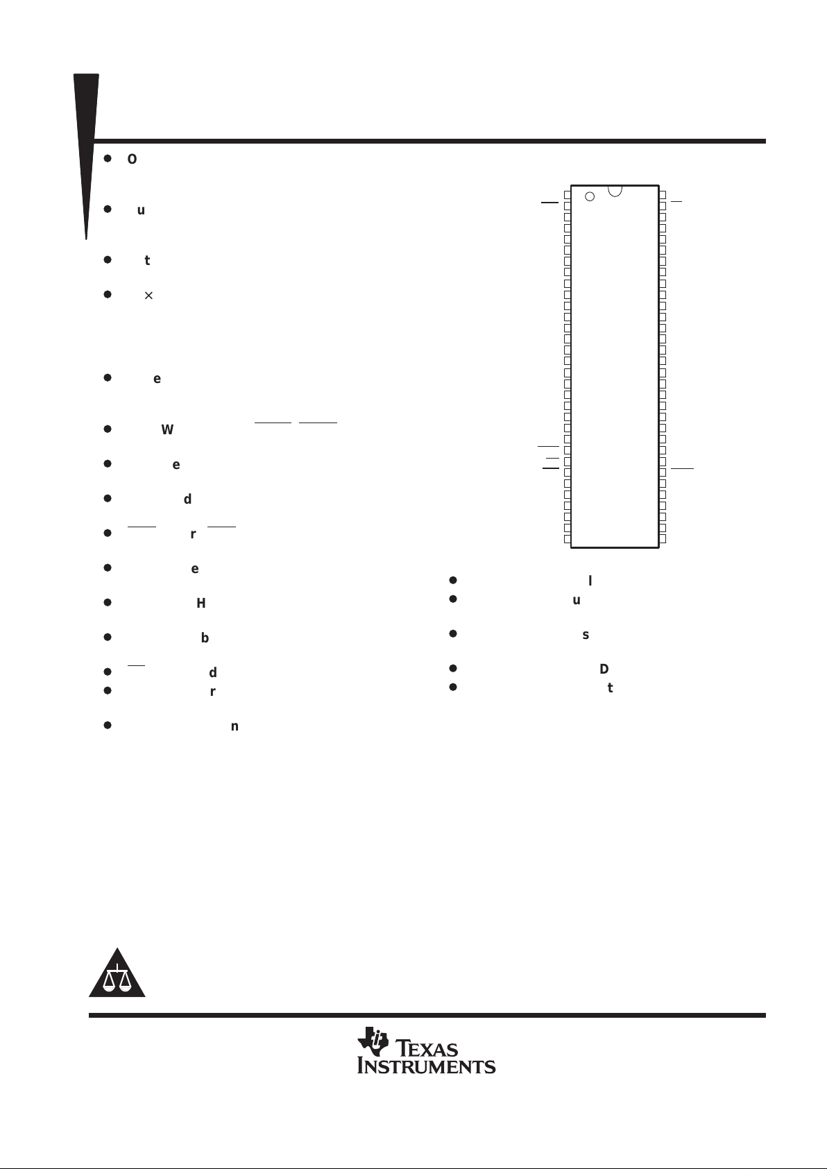
HKC PACKAGE
(TOP VIEW)
PRODUCTION DATA information is current as of publication date.
Products conform to specifications per the terms of Texas Instruments
standard warranty. Production processing does not necessarily include
testing of all parameters.
Copyright 1997, Texas Instruments Incorporated
Please be aware that an important notice concerning availability, standard warranty, and use in critical applications of
Texas Instruments semiconductor products and disclaimers thereto appears at the end of this data sheet.
SMJ55161
262144 BY 16-BIT
MULTIPORT VIDEO RAM
SGMS056D – MA Y 1995 – REVISED OCT OBER 1997
2
POST OFFICE BOX 1443 • HOUSTON, TEXAS 77251–1443
98765432
J
H
G
F
E
D
C
B
A
1
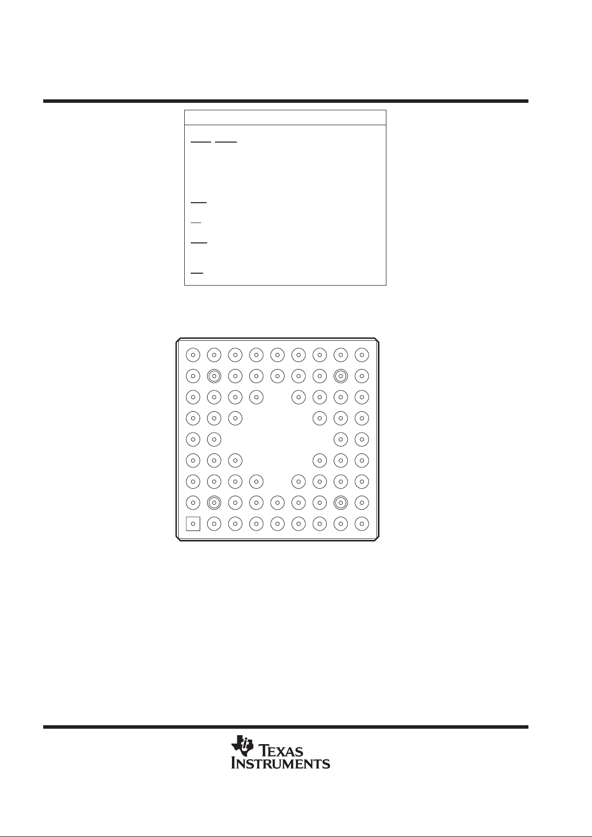
GB PACKAGE
(BOTTOM VIEW)
PIN NOMENCLATURE
A0–A8 Address Inputs
CASL
, CASU Column-Address Strobe/Byte Selects
DQ0 –DQ15 DRAM Data I/O, Write Mask Data
DSF Special-Function Select
NC/GND No Connect/Ground (Important: Not
connected internally to VSS)
QSF Special-Function Output
RAS Row-Address Strobe
SC Serial Clock
SE Serial Enable
SQ0–SQ15 Serial-Data Output
TRG Output Enable, Transfer Select
V
CC
5-V Supply (TYP)
V
SS
Ground
WE
DRAM Write-Enable Select
SMJ55161
262144 BY 16-BIT
MULTIPORT VIDEO RAM
SGMS056D – MA Y 1995 – REVISED OCT OBER 1997
3
POST OFFICE BOX 1443 • HOUSTON, TEXAS 77251–1443
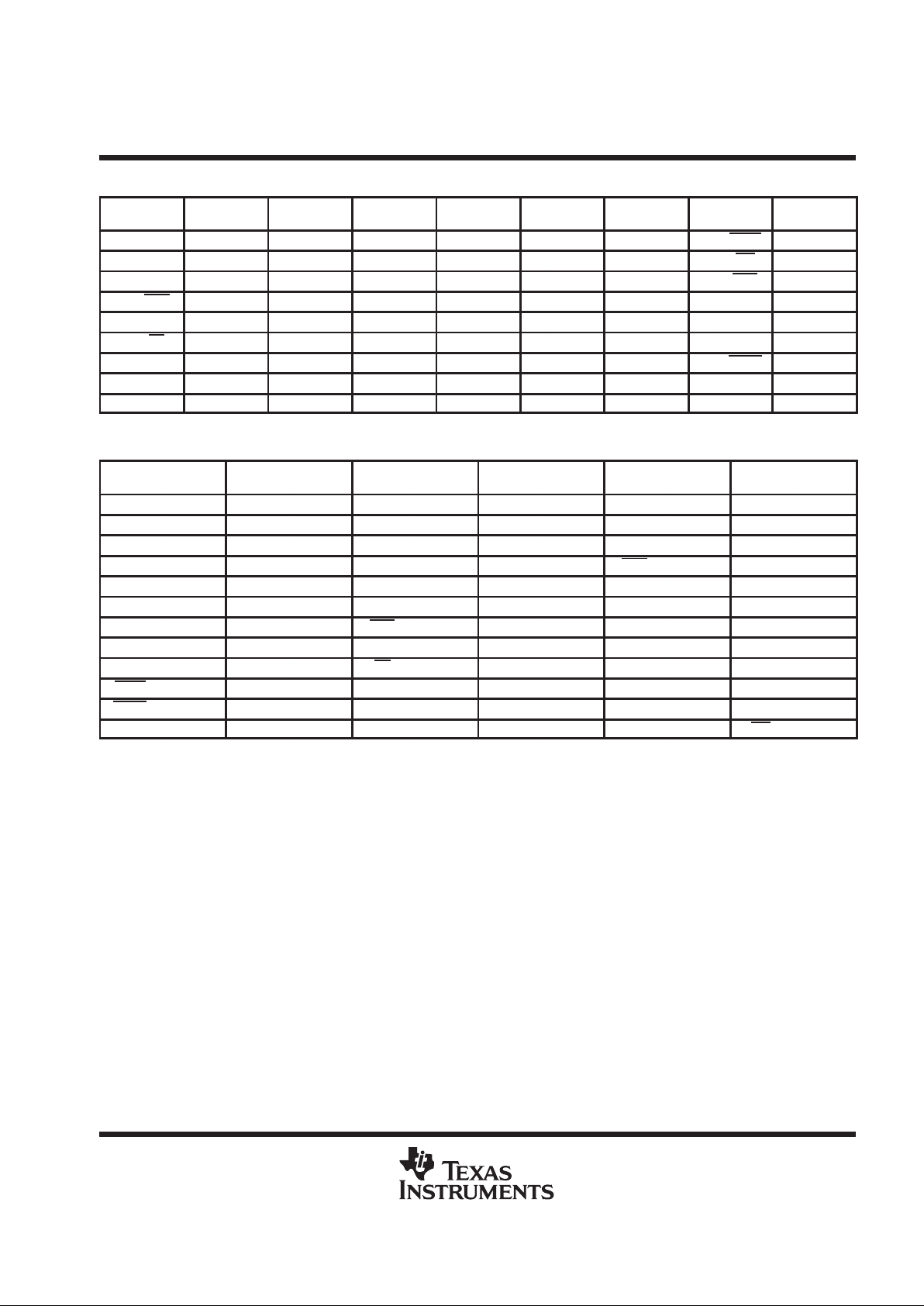
GB Package Pin Assignments – By Location
PIN PIN PIN PIN PIN PIN PIN PIN PIN
NO. NAME NO. NAME NO. NAME NO. NAME NO. NAME NO. NAME NO. NAME NO. NAME NO. NAME
J1 DQ1 J2 SQ3 J3 DQ3 J4 DQ4 J5 DQ5 J6 DQ6 J7 SQ7 J8 CASL J9 A8
H1 DQ0 H2 SQ2 H3 DQ2 H4 SQ4 H5 SQ5 H6 SQ6 H7 DQ7 H8 WE H9 A7
G1 SQ0 G2 SQ1 G3 V
DD2
G4 V
SS2
G6 V
DD2
G7 V
SS2
G8 RAS G9 A6
F1 TRG F2 V
SS1
F3 V
DD1
F7 V
DD1
F8 V
DD1
F9 A5
E1 SC E2 V
DD1
E8 V
SS1
E9 A4
D1 SE D2 V
SS1
D3 V
DD1
D7 V
SS1
D8 A3 D9 A2
C1 SQ15 C2 V
SS1
C3 V
DD2
C4 V
SS2
C6 V
DD2
C7 V
SS2
C8 CASU C9 A1
B1 DQ15 B2 DQ14 B3 DQ13 B4 DQ12 B5 DQ11 B6 DQ10 B7 SQ8 B8 DSF B9 A0
A1 SQ14 A2 SQ13 A3 SQ12 A4 SQ11 A5 SQ10 A6 SQ9 A7 DQ9 A8 DQ8 A9 QSF
GB Package Pin Assignments – By Signal
PIN PIN PIN PIN PIN PIN
NAME NO. NAME NO. NAME NO. NAME NO. NAME NO. NAME NO.
A0 B9 DQ1 J1 DQ12 B4 SQ2 H2 SQ13 A2 V
DD2
G6
A1 C9 DQ2 H3 DQ13 B3 SQ3 J2 SQ14 A1 V
DD2
C6
A2 D9 DQ3 J3 DQ14 B2 SQ4 H4 SQ15 C1 V
SS1
F2
A3 D8 DQ4 J4 DQ15 B1 SQ5 H5 TRG F1 V
SS1
D2
A4 E9 DQ5 J5 DSF B8 SQ6 H6 V
DD1
E2 V
SS1
C2
A5 F9 DQ6 J6 QSF A9 SQ7 J7 V
DD1
F3 V
SS1
D7
A6 G9 DQ7 H7 RAS G8 SQ8 B7 V
DD1
D3 V
SS1
E8
A7 H9 DQ8 A8 SC E1 SQ9 A6 V
DD1
F7 V
SS2
G4
A8 J9 DQ9 A7 SE D1 SQ10 A5 V
DD1
F8 V
SS2
C4
CASL J8 DQ10 B6 SQ0 G1 SQ11 A4 V
DD2
G3 V
SS2
G7
CASU C8 DQ11 B5 SQ1 G2 SQ12 A3 V
DD2
C3 V
SS2
C7
DQ0 H1 WE H8

SMJ55161
262144 BY 16-BIT
MULTIPORT VIDEO RAM
SGMS056D – MA Y 1995 – REVISED OCT OBER 1997
4
POST OFFICE BOX 1443 • HOUSTON, TEXAS 77251–1443
description
The SMJ55161 multiport-video random-access memory (RAM) is a high-speed, dual-port memory device. It
consists of a dynamic RAM (DRAM) module organized as 262 144 words of 16 bits each interfaced to a
serial-data register (serial-access memory [SAM]) organized as 256 words of 16 bits each. The SMJ55161
supports three basic types of operation: random access to and from the DRAM, serial access from the serial
register, and transfer of data from any row in the DRAM to the serial register . Except during transfer operations,
the SMJ55161 can be accessed simultaneously and asynchronously from the DRAM and SAM ports.
The SMJ55161 is equipped with several features designed to provide higher system-level bandwidth and to
simplify design integration on both the DRAM and SAM ports. On the DRAM port, greater pixel-draw rates are
achieved by the device’s (4 × 4) × 4 block-write feature. The block-write mode allows 16 bits of data (present
in an on-chip color-data register) to be written to any combination of four adjacent column-address locations.
As many as 64 bits of data can be written to memory during each CAS
cycle time. Also, on the DRAM port, a
write mask or a write-per-bit feature allows masking of any combination of the 16 inputs/outputs on any write
cycle. The persistent write-per-bit feature uses a mask register that, once loaded, can be used on subsequent
write cycles without reloading. The SMJ55161 also offers byte control which can be applied in read cycles, write
cycles, block-write cycles, load-write-mask-register cycles, and load-color-register cycles. The SMJ55161 also
offers extended-data-output (EDO) mode. The EDO mode is effective in both the page-mode and standard
DRAM cycles.
The SMJ55161 offers a split-register-transfer read (DRAM-to-SAM) feature for the serial register (SAM port)
that enables real-time-register-load implementation for continuous serial-data streams without critical timing
requirements. The register is divided into a high half and a low half. While one half is being read out of the SAM
port, the other half can be loaded from the memory array . For applications not requiring real-time register load
(for example, loads done during CRT -retrace periods), the full-register mode of operation is retained to simplify
system design.
The SAM port is designed for maximum performance. Data can be accessed from the SAM at serial rates up
to 45 MHz. During the split-register-transfer read operations, internal circuitry detects when the last bit position
is accessed from the active half of the register and immediately transfers control to the opposite half. A separate
output, QSF, is included to indicate which half of the serial register is active.
All inputs, outputs, and clock signals on the SMJ55161 are compatible with Series 74 TTL. All address lines and
data-in lines are latched on-chip to simplify system design. All data-out lines are unlatched to allow greater
system flexibility .
The SMJ55161 is offered in a 68-pin ceramic pin-grid-array package (GB suffix) and a 64-pin ceramic flatpack
(HKC suffix).
The SMJ55161 and other TI multiport-video RAMs are supported by a broad line of graphic processors and
control devices from TI. See Table 2 and Table 4 for additional information.
SMJ55161
262144 BY 16-BIT
MULTIPORT VIDEO RAM
SGMS056D – MA Y 1995 – REVISED OCT OBER 1997
5
POST OFFICE BOX 1443 • HOUSTON, TEXAS 77251–1443
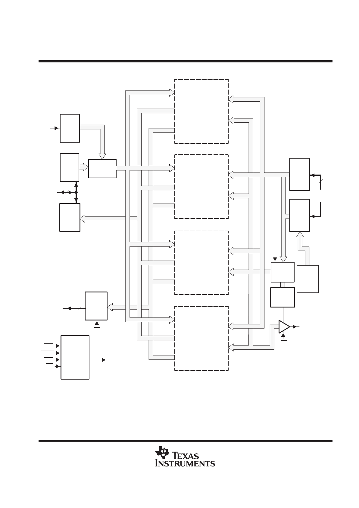
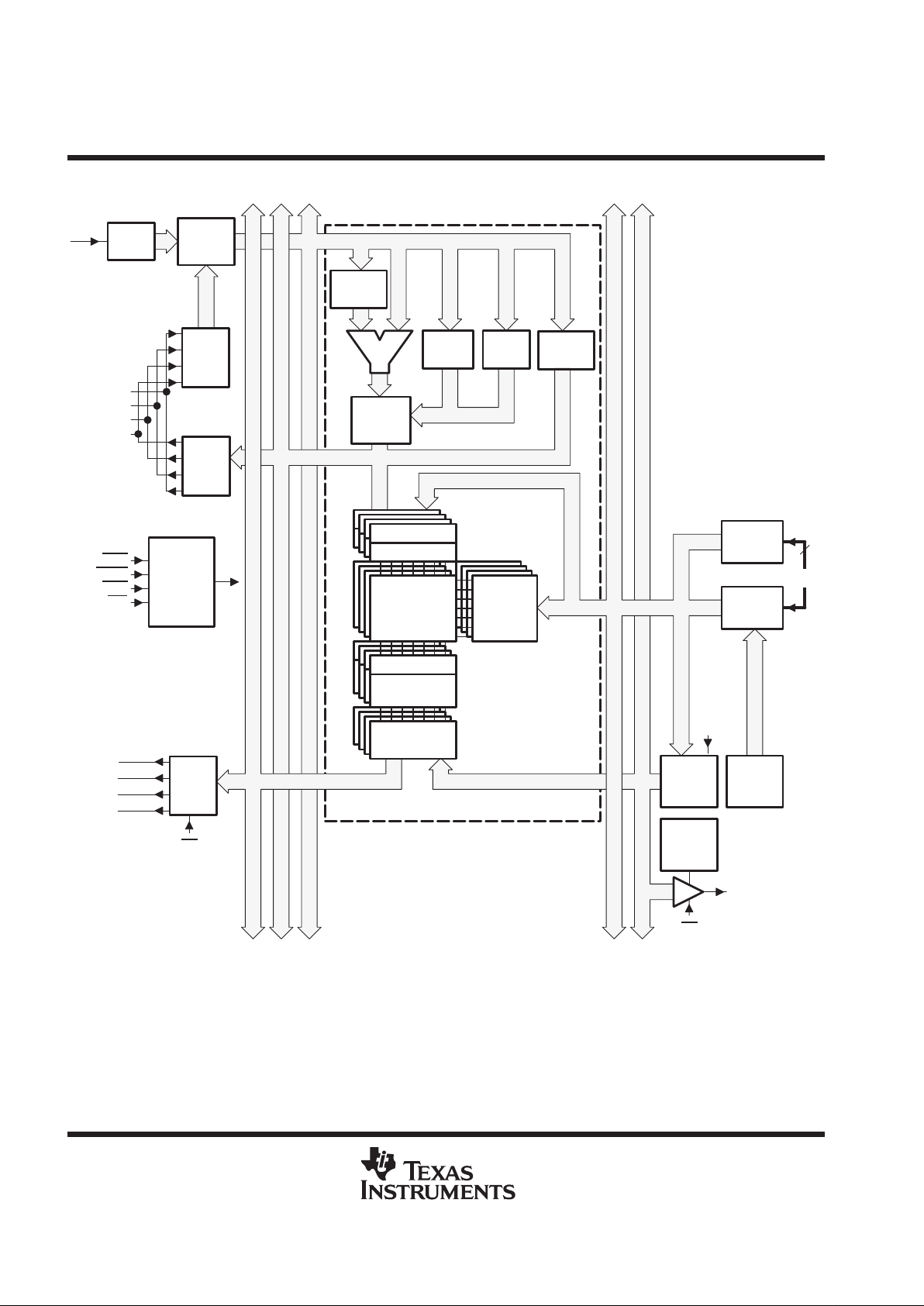
functional block diagram
Split-
Register
Status
SerialAddress
Counter
DRAM
Output
Buffer
DRAM
Input
Buffer
Input
Buffer
Row
Buffer
Column
Buffer
DQ0–
DQ15 A0–A8
DSF
1 of 4 Subblocks
(see next page)
1 of 4 Subblocks
(see next page)
1 of 4 Subblocks
(see next page)
1 of 4 Subblocks
(see next page)
QSF
SE
RAS
CASx
WE
TRG
Special-
Function
Logic
Refresh
Counter
Serial-
Output
Buffer
Timing
Generator
SQ0–
SQ15
SC
SE
16
16
9
SMJ55161
262144 BY 16-BIT
MULTIPORT VIDEO RAM
SGMS056D – MA Y 1995 – REVISED OCT OBER 1997
6
POST OFFICE BOX 1443 • HOUSTON, TEXAS 77251–1443
functional block diagram (continued)
SE
1 of 4 Subblocks
Refresh
Counter
Row
Decoder
Split-
Register
Status
SerialAddress
Counter
Color
Register
Address
Mask
W/B
Latch
W/B
Unlatch
MUX
Write-
Per-Bit
Control
Serial-Data
Pointer
Serial-Data
Register
512 × 512
Memory
Array
Sense AMP
Column DEC
Special-
Function
Logic
Input
Buffer
DQi
DQi+1
DQi+2
DQi+3
RAS
CASx
TRG
WE
Column
Buffer
A0–A8
DSF
Row
Buffer
QSF
DRAM
Output
Buffer
DRAM
Input
Buffer
Timing
Generator
SQi
SQi + 1
SQi +2
SQi + 3
Serial-
Output
Buffer
SE
SC
9
SMJ55161
262144 BY 16-BIT
MULTIPORT VIDEO RAM
SGMS056D – MA Y 1995 – REVISED OCT OBER 1997
7
POST OFFICE BOX 1443 • HOUSTON, TEXAS 77251–1443
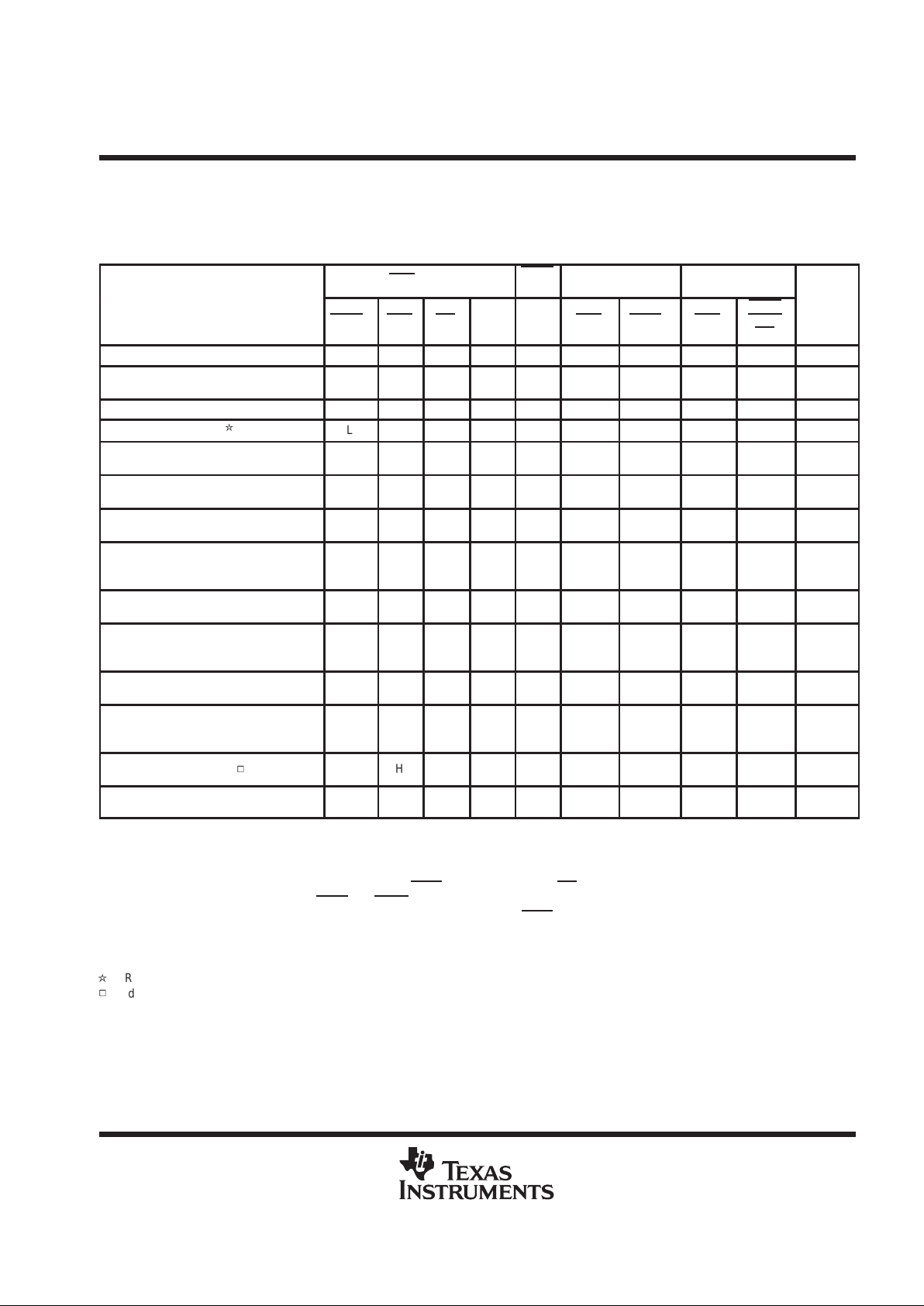
functional operation description
Table 1 lists the DRAM and SAM functions, summarizing Table 3 and Table 4.
Table 1. DRAM and SAM Functions
RAS FALL
CASx
FALL
ADDRESS DQ0 –DQ15
†
FUNCTION
CASx‡TRG WE DSF DSF RAS CASx
§
RAS
CASL
CASU
WE
MNE
CODE
Reserved (do not use) L L L L X X X X X —
CBR refresh (no reset) and stop-point
set
¶
L X L H X
Stop
Point
#
X X X CBRS
CBR refresh (option reset)
||
L X H L X X X X X CBR
CBR refresh (no reset)
k
L X H H X X X X X CBRN
Full-register-transfer read H L H L X
Row
Address
Tap
Point
X X RT
Split-register-transfer read H L H H X
Row
Address
Tap
Point
X X SRT
DRAM write
(nonpersistent write-per-bit)
H H L L L
Row
Address
Column
Address
Write
Mask
Valid
Data
RWM
DRAM block write
(nonpersistent write-per-bit)
H H L L H
Row
Address
Block
Address
A2–A8
Write
Mask
Column
Mask
BWM
DRAM write
(persistent write-per-bit)
H H L L L
Row
Address
Column
Address
X
Valid
Data
RWM
DRAM block write
(persistent write-per-bit)
H H L L H
Row
Address
Block
Address
A2–A8
X
Column
Mask
BWM
DRAM write (nonmasked) H H H L L
Row
Address
Column
Address
X
Valid
Data
RW
DRAM block write (nonmasked) H H H L H
Row
Address
Block
Address
A2–A8
X
Column
Mask
BW
Load write-mask register
h
H H H H L
Refresh
Address
X X
Write
Mask
LMR
Load color register H H H H H
Refresh
Address
X X
Color
Data
LCR
Legend:
Col Mask = H: Write to address/column enabled
Write Mask = H: Write to I/O enabled
X = Don’t care
†
DQ0–DQ15 are latched on either the first falling edge of CASx
or the falling edge of WE, whichever occurs later.
‡
Logic L is selected when either or both CASL
and CASU are low.
§
The column address and block address are latched on the first falling edge of CASx
.
¶
CBRS cycle should be performed immediately after the powerup initialization cycle.
#
A0–A3, A8: don’t care; A4–A7: stop-point code
||
CBR refresh (option reset) mode ends persistent write-per-bit mode and stop-point mode.
k
CBR refresh (no reset) mode does not end persistent write-per-bit mode or stop-point mode.
h
Load-write-mask-register cycle sets the persistent write-per-bit mode. The persistent write-per-bit mode is reset only by the CBR (option reset)
cycle.
SMJ55161
262144 BY 16-BIT
MULTIPORT VIDEO RAM
SGMS056D – MA Y 1995 – REVISED OCT OBER 1997
8
POST OFFICE BOX 1443 • HOUSTON, TEXAS 77251–1443
pin definitions
Table 2. Pin Description Versus Operational Mode
PIN DRAM TRANSFER SAM
A0 –A8 Row, column address Row address, tap point
CASL
CASU
Column-address strobe, DQ output enable Tap-address strobe
DQ DRAM data I/O, write mask
DSF
Block-write enable
Write-mask-register load enable
Color-register load enable
CBR (option reset)
Split-register-transfer enable
RAS Row-address strobe Row-address strobe
SE
SQ output enable,
QSF output enable
SC Serial clock
SQ Serial-data output
TRG DQ output enable Transfer enable
WE Write enable, write-per-bit enable
QSF Special-function output Serial-register status
NC/GND Either make no external connection or tie to system GND (VSS)
V
CC
†
5-V supply
V
SS
†
Ground
†
For proper device operation, all VCC pins must be connected to a 5-V supply, and all VSS pins must be tied to ground.
address (A0–A8)
Eighteen address bits are required to decode each one of the 262 144 storage cell locations. Nine row-address
bits are set up on pins A0–A8 and latched onto the chip on the falling edge of RAS
. Nine column-address bits
are set up on pins A0–A8 and latched onto the chip on the first falling edge of CASx
. All addresses must be
stable on or before the falling edge of RAS
and the first falling edge of CASx.
During the full-register-transfer read operation, the states of A0–A8 are latched on the falling edge of RAS
to
select one of the 512 rows where the transfer occurs. At the first falling edge of CASx
, the column-address bits
A0–A8 are latched. The most significant column-address bit (A8) selects which half of the row is transferred
to the SAM. The appropriate 8-bit column address (A0–A7) selects one of 256 tap points (starting positions)
for the serial-data output.
During the split-register-transfer read operation, address bit A7 is ignored at the falling edge of CASx
. An internal
counter selects which half of the register is used. If the high half of the SAM is currently in use, the low half of
the SAM is loaded with the low half of the DRAM half row and vice versa. Column address (A8) selects the DRAM
half row. The remaining seven address bits (A0–A6) are used to select one of 127 possible starting locations
within the SAM. Locations 127 and 255 are not valid tap points.
row-address strobe (RAS
)
RAS
is similar to a chip enable so that all DRAM cycles and transfer cycles are initiated by the falling edge of
RAS
. RAS is a control input that latches the states of the row address, WE, TRG, CASL, CASU, and DSF onto
the chip to invoke DRAM and transfer-read functions of the SMJ55161.

SMJ55161
262144 BY 16-BIT
MULTIPORT VIDEO RAM
SGMS056D – MA Y 1995 – REVISED OCT OBER 1997
9
POST OFFICE BOX 1443 • HOUSTON, TEXAS 77251–1443
column-address strobe (CASL, CASU)
CASL
and CASU are control inputs that latch the states of the column address and DSF to control DRAM and
transfer functions of the SMJ55161. CASx
also acts as output enable for the DRAM output pins DQ0–DQ15.
In DRAM operation, CASL
enables data to be written to or read from the lower byte (DQ0–DQ7), and CASU
enables data to be written to or from the upper byte (DQ8–DQ15). In transfer operations, address bits A0–A8
are latched at the first falling edge of CASx
as the start position (tap) for the serial-data output (SQ0–SQ15).
output enable/transfer select (TRG
)
TRG
selects either DRAM or transfer operation as RAS falls. For DRAM operation, TRG must be held high as
RAS
falls. During DRAM operation, TRG functions as an output enable for the DRAM output pins DQ0–DQ15.
For transfer operation, TRG
must be brought low before RAS falls.
write-mask select, write enable (WE
)
In DRAM operation, WE
enables data to be written to the DRAM. WE is also used to select the DRAM
write-per-bit mode. Holding WE
low on the falling edge of RAS invokes the write-per-bit operation. The
SMJ55161 supports both the nonpersistent write-per-bit mode and the persistent write-per-bit mode.
special-function select (DSF)
The DSF input is latched on the falling edge of RAS
or the first falling edge of CASx, similar to an address. DSF
determines which of the following functions are invoked on a particular cycle:
D
CBR refresh with reset (CBR)
D
CBR refresh with no reset (CBRN)
D
CBR refresh with no reset and stop-point set (CBRS)
D
Block write
D
Loading write-mask register for the persistent write-per-bit mode (LMR)
D
Loading color register for the block-write mode
D
Split-register-transfer read
DRAM data I/O, write mask data (DQ0–DQ15)
DRAM data is written or read through the common I/O DQ pins. The 3-state DQ-output buffers provide direct
TTL compatibility (no pullup resistors) with a fanout of one Series 54 TTL load. Data out is the same polarity
as data in. During a normal access cycle, the outputs remain in the high-impedance state until TRG
is brought
low. Data appears at the outputs until TRG
returns high, CASx returns high following RAS returning high, or RAS
returns high following CASx returning high. The write mask is latched into the device through the random DQ
pins by the falling edge of RAS
and is used on all write-per-bit cycles. In a transfer operation, the DQ outputs
remain in the high-impedance state for the entire cycle.
serial-data outputs (SQ0 –SQ15)
Serial data is read from the SQ pins. The SQ output buffers provide direct TTL compatibility (no pullup resistors)
with a fanout of one Series 54 TTL load. The serial outputs are in the high-impedance (floating) state as long
as the serial-enable pin, SE
, is high. The serial outputs are enabled when SE is brought low.
serial clock (SC)
Serial data is accessed out of the data register during the rising edge of SC. The SMJ55161 is designed to work
with a wide range of clock duty cycles to simplify system design. There is no refresh requirement because the
data registers that comprise the SAM are static. There is also no minimum SC-clock operating frequency.

SMJ55161
262144 BY 16-BIT
MULTIPORT VIDEO RAM
SGMS056D – MA Y 1995 – REVISED OCT OBER 1997
10
POST OFFICE BOX 1443 • HOUSTON, TEXAS 77251–1443
serial enable (SE)
During serial-access operations, SE
is used as an enable / disable for the SQ outputs. SE low enables the
serial-data output while SE
high disables the serial-data output. SE is also used as an enable/disable for output
pin QSF.
IMPORT ANT: While SE
is held high, the serial clock is not disabled. External SC pulses increment the internal
serial-address counter regardless of the state of SE
. This ungated serial-clock scheme minimizes access time
of serial output from SE
low because the serial-clock input buffer and the serial-address counter are not disabled
by SE
.
special-function output (QSF)
QSF is an output pin that indicates which half of the SAM is being accessed. When QSF is low, the serial-address
pointer is accessing the lower (least significant) 128 bits of the serial register (SAM). When QSF is high, the
pointer is accessing the higher (most significant) 128 bits of the SAM.
During full-register-transfer operations, QSF can change state upon completing the cycle. This state is
determined by the tap point loaded during the transfer cycle. QSF is enabled by SE
; therefore, if SE is high, the
QSF output is in the high-impedance state.
no connect /ground (NC/GND)
NC/GND must be tied to system ground or left floating for proper device operation.
SMJ55161
262144 BY 16-BIT
MULTIPORT VIDEO RAM
SGMS056D – MA Y 1995 – REVISED OCT OBER 1997
11
POST OFFICE BOX 1443 • HOUSTON, TEXAS 77251–1443
random access operation
Table 3 lists the DRAM functions.
Table 3. DRAM Functions
RAS FALL
CASx
FALL
ADDRESS DQ0 –DQ15
†
FUNCTION
CASx‡TRG WE DSF DSF RAS CASx
§
RAS
CASL
CASU
WE
MNE
CODE
Reserved (do not use) L L L L X X X X X —
CBR refresh (no reset) and stop-point
set
¶
L X L H X
Stop
Point
#
X X X CBRS
CBR refresh (option reset)
||
L X H L X X X X X CBR
CBR refresh (no reset)
k
L X H H X X X X X CBRN
DRAM write
(nonpersistent write-per-bit)
H H L L L
Row
Address
Column
Address
Write
Mask
Valid
Data
RWM
DRAM block write
(nonpersistent write-per-bit)
H H L L H
Row
Address
Block
Address
A2–A8
Write
Mask
Column
Mask
BWM
DRAM write
(persistent write-per-bit)
H H L L L
Row
Address
Column
Address
X
Valid
Data
RWM
DRAM block write
(persistent write-per-bit)
H H L L H
Row
Address
Block
Address
A2–A8
X
Column
Mask
BWM
DRAM write (nonmasked) H H H L L
Row
Address
Column
Address
X
Valid
Data
RW
DRAM block write (nonmasked) H H H L H
Row
Address
Block
Address
A2–A8
X
Column
Mask
BW
Load write-mask register
h
H H H H L
Refresh
Address
X X
Write
Mask
LMR
Load color register H H H H H
Refresh
Address
X X
Color
Data
LCR
Legend:
Col Mask = H: Write to address/column enabled
Write Mask = H: Write to I/O enabled
X = Don’t care
†
DQ0–DQ15 are latched on either the first falling edge of CASx
or the falling edge of WE, whichever occurs later.
‡
Logic L is selected when either or both CASL
and CASU are low.
§
The column address and block address are latched on the first falling edge of CASx
.
¶
CBRS cycle should be performed immediately after the power-up initialization cycle.
#
A0–A3, A8: don’t care; A4–A7: stop-point code
||
CBR refresh (option reset) mode ends persistent write-per-bit mode and stop-point mode.
k
CBR refresh (no reset) mode does not end persistent write-per-bit mode or stop-point mode.
h
Load-write-mask-register cycle sets the persistent write-per-bit mode. The persistent write-per-bit mode is reset only by the CBR (option reset)
cycle.

SMJ55161
262144 BY 16-BIT
MULTIPORT VIDEO RAM
SGMS056D – MA Y 1995 – REVISED OCT OBER 1997
12
POST OFFICE BOX 1443 • HOUSTON, TEXAS 77251–1443
enhanced page mode
Enhanced page-mode operation allows faster memory access by keeping the same row address while selecting
random column addresses. This mode eliminates the time required for row-address setup, row-address hold,
and address multiplex. The maximum RAS
low time and CAS page cycle time used determine the number of
columns that can be accessed.
Unlike conventional page-mode operations, the enhanced page mode allows the SMJ55161 to operate at a
higher data bandwidth. Data retrieval begins as soon as the column address is valid rather than when CASx
transitions low. A valid column address can be presented immediately after the row-address hold time has been
satisfied, usually well in advance of the falling edge of CASx
. In this case, data is obtained after t
a(C)
MAX
(access time from CASx
low) if t
a(CA)
MAX (access time from column address) has been satisfied.
refresh
CAS-before-RAS (CBR) refresh
CBR refreshes are accomplished by bringing either or both CASL and CASU low earlier than RAS. The external
row address is ignored, and the refresh row address is generated internally . Three types of CBR refresh cycles
are available. The CBR refresh (option reset) ends the persistent write-per-bit mode and the stop-point mode.
The CBRN and CBRS refreshes (no reset) do not end the persistent write-per-bit mode or the stop-point mode.
The 512 rows of the DRAM do not necessarily need to be refreshed consecutively as long as the entire refresh
is completed within the required time period, t
rf(MA)
. The output buffers remain in the high-impedance state
during the CBR refresh cycles regardless of the state of TRG
.
hidden refresh
A hidden refresh is accomplished by holding both CASL and CASU low in the DRAM read cycle and cycling
RAS
. The output data of the DRAM read cycle remains valid while the refresh is carried out. Like the CBR
refresh, the refreshed row addresses are generated internally during the hidden refresh.
RAS-only refresh
A RAS-only refresh is accomplished by cycling RAS at every row address. Unless CASx and TRG are low, the
output buffers remain in the high-impedance state to conserve power. Externally-generated addresses must
be supplied during RAS
-only refresh. Strobing each of the 512 row addresses with RAS causes all bits in each
row to be refreshed.
SMJ55161
262144 BY 16-BIT
MULTIPORT VIDEO RAM
SGMS056D – MA Y 1995 – REVISED OCT OBER 1997
13
POST OFFICE BOX 1443 • HOUSTON, TEXAS 77251–1443
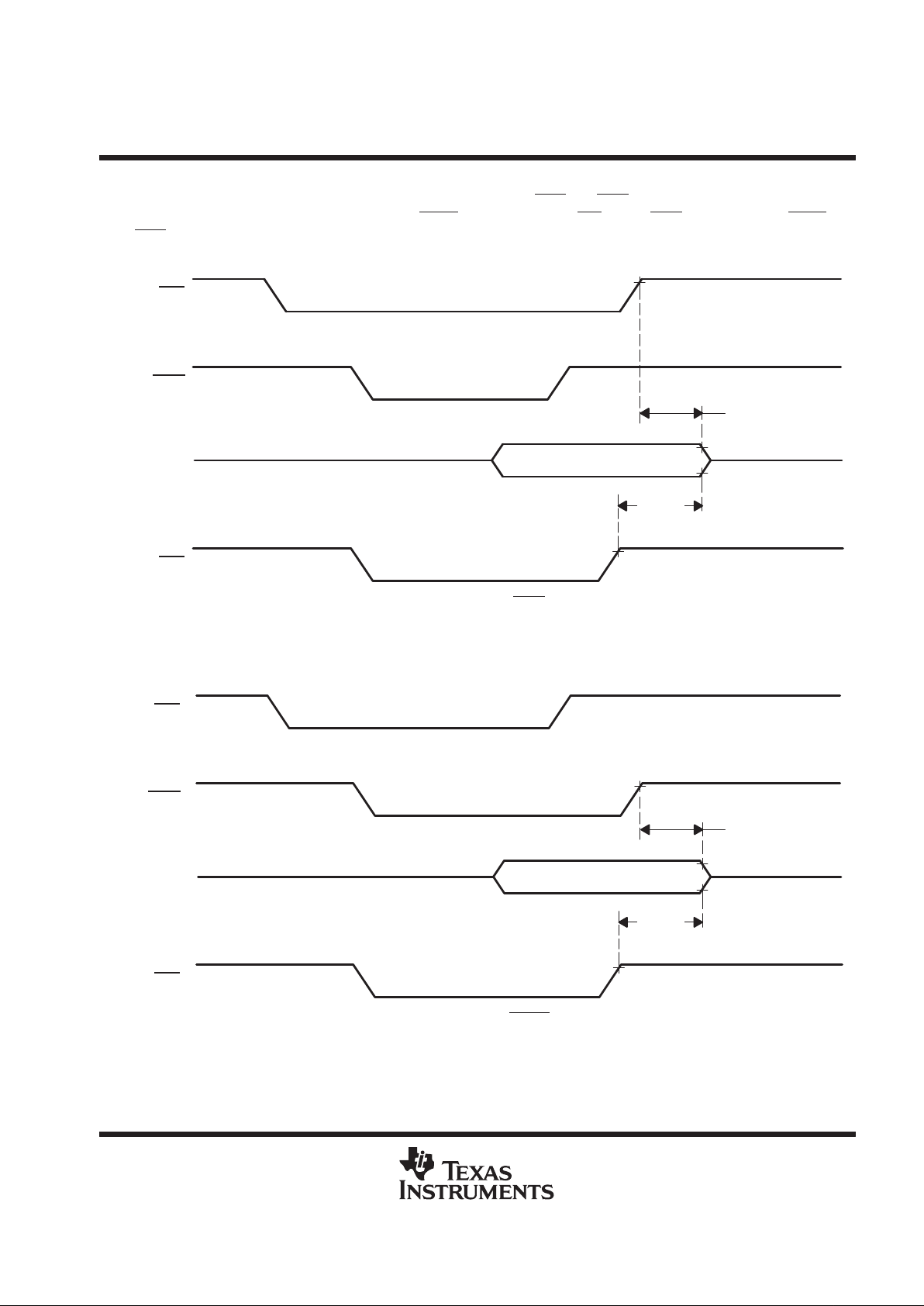
extended data output
The SMJ55161 features EDO during DRAM accesses. While RAS
and TRG are low, the DRAM output remains
valid. The output remains valid even when CASx
returns high until WE is low, TRG is high, or both CASx and
RAS
are high (see Figure 1 and Figure 2). The EDO mode functions during all read cycles including DRAM read,
page-mode read, and read-modify-write cycles (see Figure 3).
RAS
CASx
DQ0–DQ15
TRG
Valid Output
t
dis(RH)
t
dis(G)
Figure 1. DRAM Read Cycle With RAS-Controlled Output
RAS
CASx
DQ0–DQ15
TRG
Valid Output
t
dis(CH)
t
dis(G)
Figure 2. DRAM Read Cycle With CASx-Controlled Output
SMJ55161
262144 BY 16-BIT
MULTIPORT VIDEO RAM
SGMS056D – MA Y 1995 – REVISED OCT OBER 1997
14
POST OFFICE BOX 1443 • HOUSTON, TEXAS 77251–1443
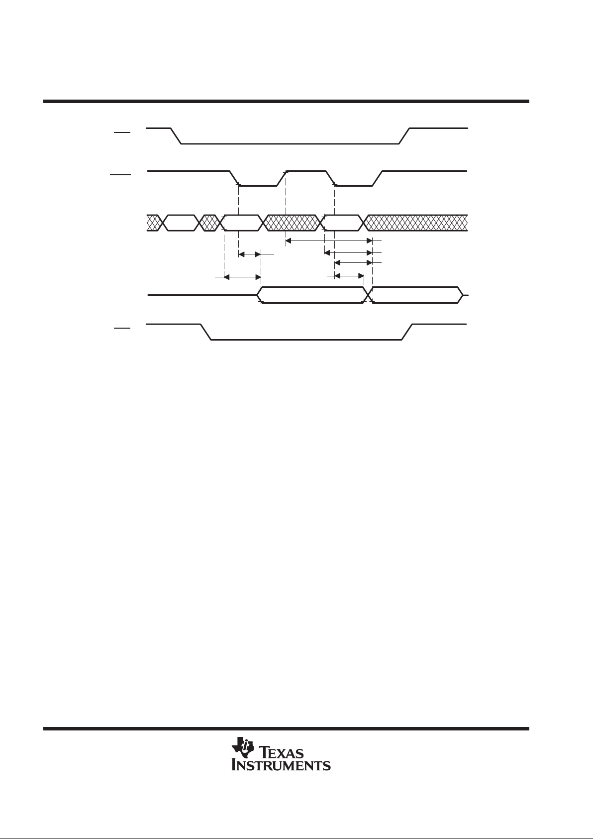
extended-data output (continued)
RAS
A0–A8
DQ0–DQ15
Valid Output
t
a(CA)
Row
CASx
TRG
Valid Output
t
a(C)
t
h(CLQ)
t
a(C)
t
a(CP)
Column Column
t
a(CA)
Figure 3. DRAM Page-Read Cycle With Extended Output
SMJ55161
262144 BY 16-BIT
MULTIPORT VIDEO RAM
SGMS056D – MA Y 1995 – REVISED OCT OBER 1997
15
POST OFFICE BOX 1443 • HOUSTON, TEXAS 77251–1443
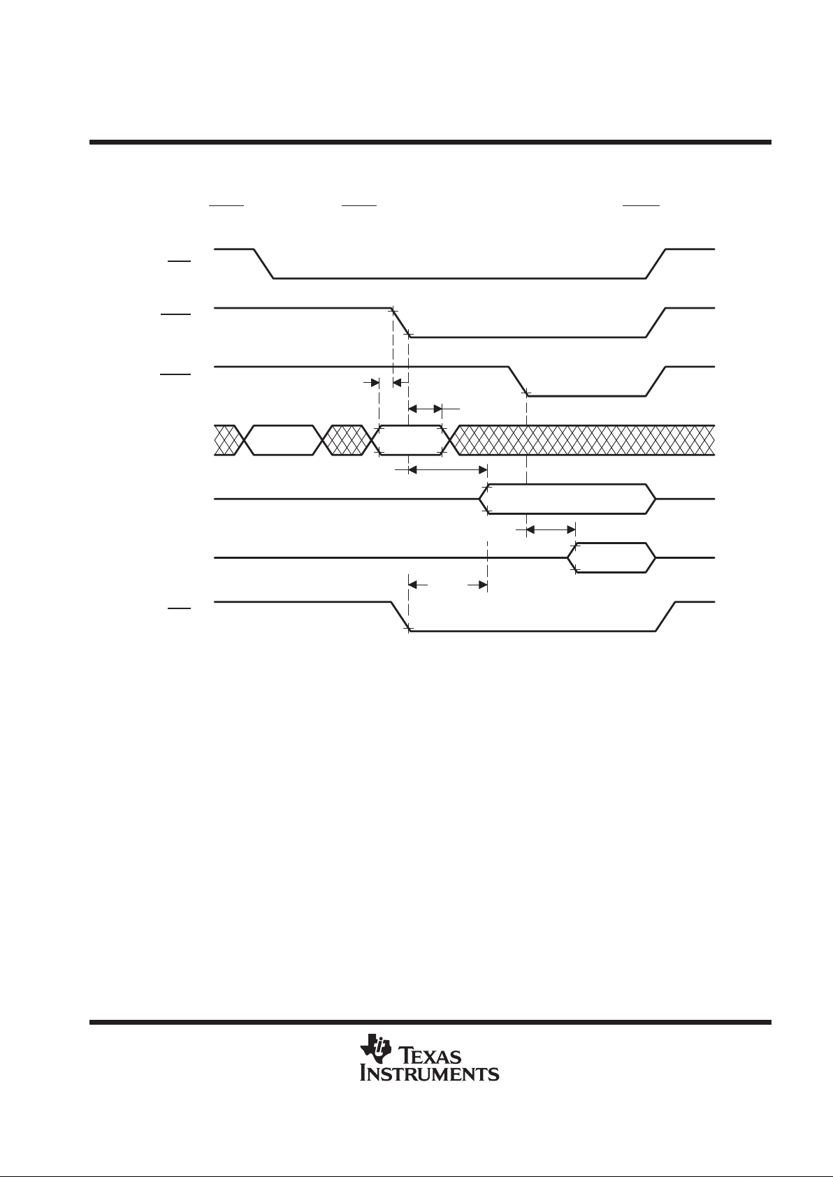
byte operation
Byte operation can be applied in DRAM-read cycles, write cycles, block-write cycles, load-write-mask-register
cycles, and load-color-register cycles. In byte operation, the column address (A0 –A8) is latched at the first
falling edge of CASx
. In read cycles, CASL enables the lower byte (DQ0–DQ7) and CASU enables the upper
byte (DQ8–DQ15) (see Figure 4).
Row
t
h(CLCA)
RAS
t
su(CA)
Column
Lower Byte Output
Upper Byte
Output
t
a(C)
CASL
CASU
A0–A8
DQ0–DQ7
DQ8–DQ15
TRG
t
a(G)
t
a(C)
Figure 4. Example of a Byte-Read Cycle
SMJ55161
262144 BY 16-BIT
MULTIPORT VIDEO RAM
SGMS056D – MA Y 1995 – REVISED OCT OBER 1997
16
POST OFFICE BOX 1443 • HOUSTON, TEXAS 77251–1443
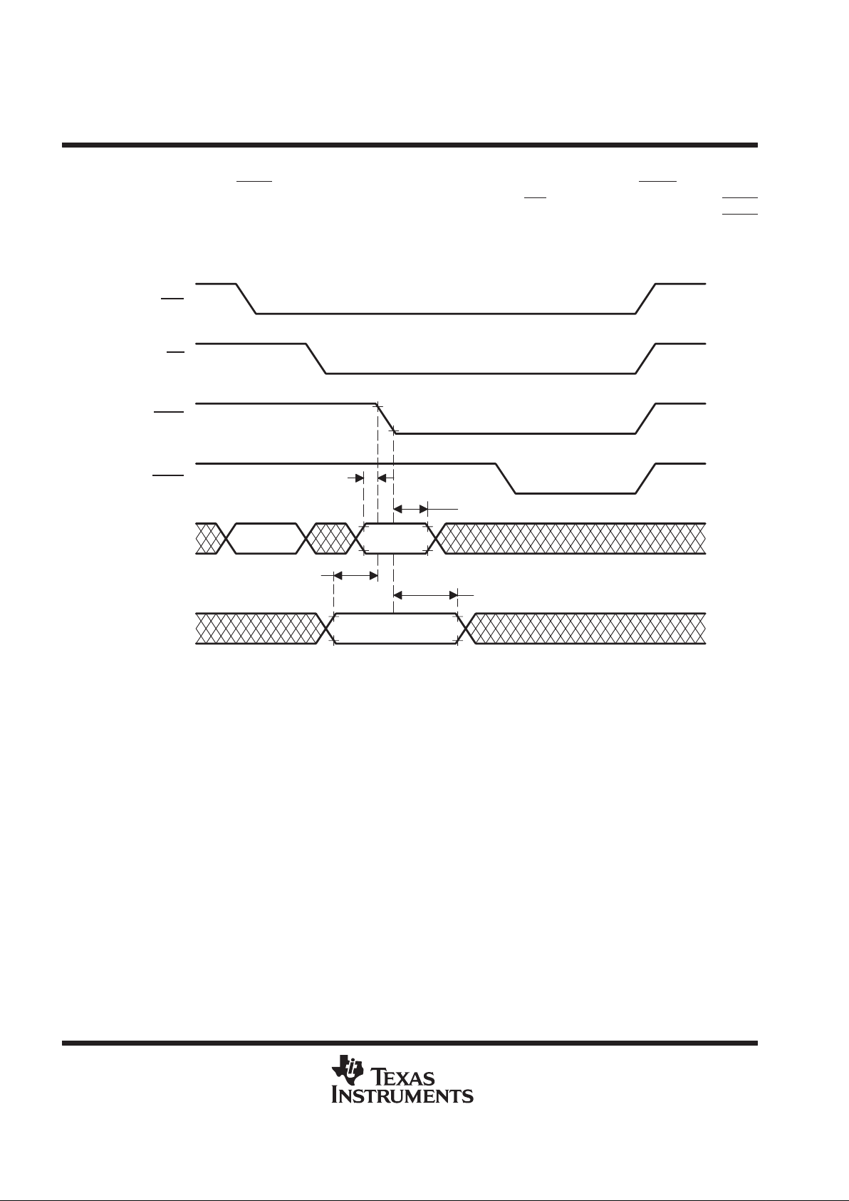
byte operation (continued)
In byte-write operation, CASL
enables data to be written to the lower byte (DQ0–DQ7), and CASU enables data
to be written to the upper byte (DQ8 –DQ15). In an early write cycle, WE
is brought low prior to both CASx
signals, and data setup and hold times for DQ0 – DQ15 are referenced to the first falling edge of CASx
(see Figure 5).
RAS
WE
CASU
A0–A8
DQ0–DQ15
Valid Input
t
h(CLD)
t
su(DCL)
CASL
t
h(CLCA)
t
su(CA)
Row Column
Figure 5. Example of an Early-Write Cycle
SMJ55161
262144 BY 16-BIT
MULTIPORT VIDEO RAM
SGMS056D – MA Y 1995 – REVISED OCT OBER 1997
17
POST OFFICE BOX 1443 • HOUSTON, TEXAS 77251–1443
byte operation (continued)
For late-write or read-modify-write cycles, WE
is brought low after either or both CASL and CASU fall. The data
is strobed in with data setup and hold times for DQ0–DQ15 referenced to WE
(see Figure 6).
RAS
CASL
CASU
WE
DQ0–DQ15
Valid Input
t
h(WLD)
t
su(DWL)
Figure 6. Example of a Late-Write Cycle
SMJ55161
262144 BY 16-BIT
MULTIPORT VIDEO RAM
SGMS056D – MA Y 1995 – REVISED OCT OBER 1997
18
POST OFFICE BOX 1443 • HOUSTON, TEXAS 77251–1443
write-per-bit
The write-per-bit feature allows masking any combination of the 16 DQs on any write cycle. The write-per-bit
operation is invoked when WE is held low on the falling edge of RAS. If WE is held high on the falling edge of
RAS
, the write operation is performed without any masking. The SMJ55161 offers two write-per-bit modes:
nonpersistent write-per-bit and persistent write-per-bit.
nonpersistent write-per-bit
When WE is low on the falling edge of RAS, the write mask is reloaded. A 16-bit binary code (the write-per-bit
mask) is input to the device through the DQ pins and latched on the falling edge of RAS
. The write-per-bit mask
selects which of the 16 I/Os are to be written and which are not. After RAS
has latched the on-chip write-per-bit
mask, input data is driven onto the DQ pins and is latched on either the first falling edge of CASx
or the falling
edge of WE
, whichever occurs later. CASL enables the lower byte (DQ0–DQ7) to be written through the mask
and CASU
enables the upper byte (DQ8–DQ15) to be written through the mask. If a data low (write mask = 0)
is strobed into a particular I /O pin on the falling edge of RAS
, data is not written to that I /O. If a data high
(write mask = 1) is strobed into a particular I / O pin on the falling edge of RAS
, data is written to that I / O
(see Figure 7).
RAS
CASL
CASU
WE
DQ0–DQ15 Valid Input
t
h(WLD)
t
su(DQR)
t
su(DWL)
t
h(RDQ)
Write Mask
Figure 7. Example of a Nonpersistent Write-Per-Bit (Late-Write) Operation
SMJ55161
262144 BY 16-BIT
MULTIPORT VIDEO RAM
SGMS056D – MA Y 1995 – REVISED OCT OBER 1997
19
POST OFFICE BOX 1443 • HOUSTON, TEXAS 77251–1443
persistent write-per-bit
The persistent write-per-bit mode is initiated by performing a load-write-mask-register (LMR) cycle. In the
persistent write-per-bit mode, the write-per-bit mask is overwritten but remains valid over an arbitrary number
of write cycles until another LMR cycle is performed or power is removed.
The LMR cycle is performed using DRAM write-cycle timing with DSF held high on the falling edge of RAS
and
held low on the first falling edge of CASx
. A binary code is input to the write-mask register via the random I/O
pins and latched on either the first falling edge of CASx
or the falling edge of WE, whichever occurs later. Byte
write control can be applied to the write mask during the LMR cycle. The persistent write-per-bit mode can then
be used in exactly the same way as the nonpersistent write-per-bit mode except that the input data on the falling
edge of RAS
is ignored. When the device is set to the persistent write-per-bit mode, it remains in this mode and
is reset only by a CBR refresh (option-reset) cycle (see Figure 8).
RAS
CASx
A0–A8
DSF
Load-Write-Mask Register Persistent Write-Per-Bit
DQ0–
DQ15
Write-Mask
Data
Valid
Input
CBR Refresh (option reset)
WE
Refresh
Address
Row Column
Mask Data = 1: Write to I/O enabled
= 0: Write to I/O disabled
Figure 8. Example of a Persistent Write-Per-Bit Operation
SMJ55161
262144 BY 16-BIT
MULTIPORT VIDEO RAM
SGMS056D – MA Y 1995 – REVISED OCT OBER 1997
20
POST OFFICE BOX 1443 • HOUSTON, TEXAS 77251–1443
block write
The block-write feature allows up to 64 bits of data to be written simultaneously to one row of the memory array .
This function is implemented as four columns by four DQs and repeated in four quadrants. In this manner, each
of the four 1M-bit quadrants can have up to four consecutive columns written at a time with up to four DQs per
column (see Figure 9).
DQ4
DQ14
DQ0
Four Consecutive Columns of 0–511
DQ1
DQ2
DQ3
DQ5
DQ6
DQ7
DQ8
DQ9
DQ10
DQ11
DQ12
DQ13
DQ15
4th Quadrant
3rd Quadrant
2nd Quadrant
1st Quadrant
One Row of 0–511
Figure 9. Block-Write Operation
Each 1M-bit quadrant has a 4-bit column mask to mask off and prevent any or all of the four columns from being
written with data. Nonpersistent write-per-bit or persistent write-per-bit functions can be applied to the
block-write operation to provide write-masking options. The DQ data is provided by 4 bits from the on-chip color
register. Bits 0–3 from the 16-bit write-mask register, bits 0–3 from the 16-bit column-mask register, and bits
0–3 from the 16-bit color-data register configure the block write for the first quadrant, while bits 4 –7, 8–11,
and 12–15 of the corresponding registers control the other quadrants in a similar fashion (see Figure 10).
 Loading...