

AUSTIN SMJ4C1024-10, SMJ4C1024-12, SMJ4C1024-80, SMJ4C1024-15 Datasheet
SMJ4C1024
1048576 BY 1-BIT
DYNAMIC RANDOM-ACCESS MEMORY
SGMS023E – DECEMBER 1988 – REVISED MARCH 1996
1
POST OFFICE BOX 1443 • HOUSTON, TEXAS 77251–1443
D
Organization...1048576 × 1-Bit
D
Processed to MIL-STD-883, Class B
D
Single 5-V Supply (10% Tolerance)
D
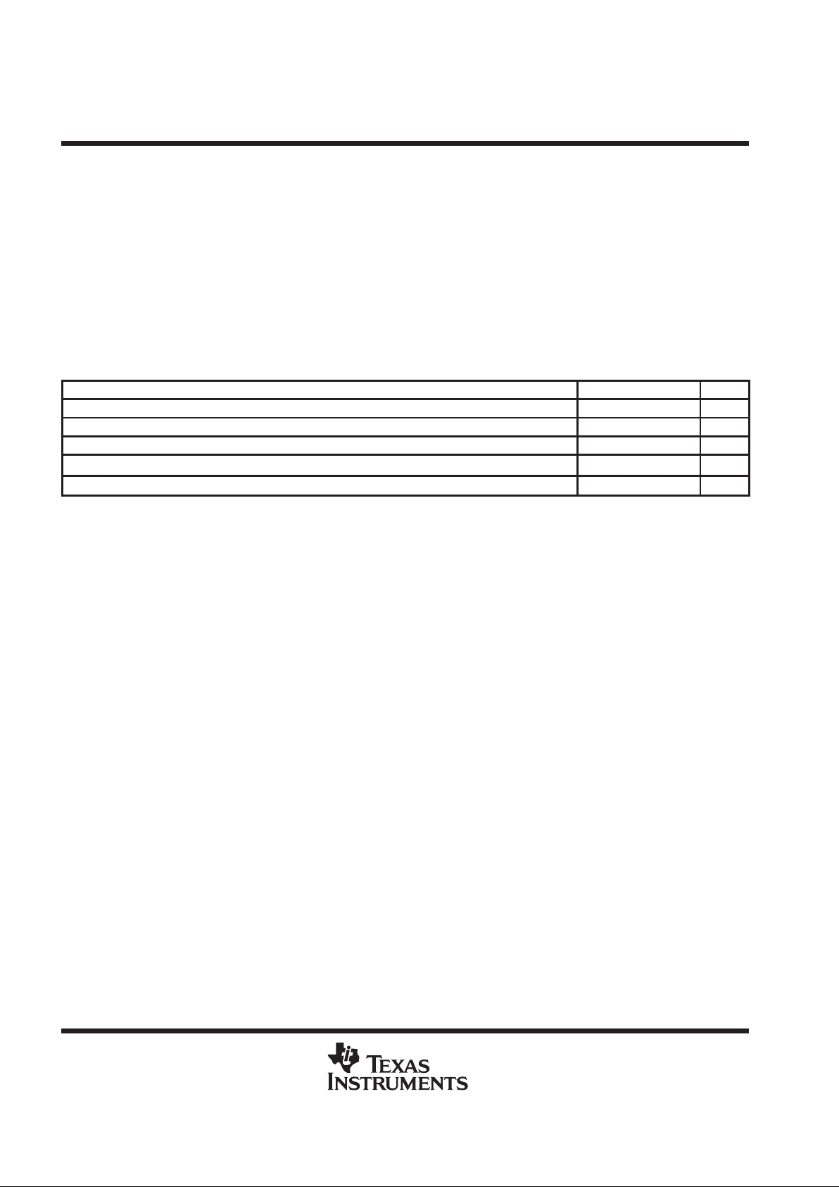
Performance Ranges:
ACCESS ACCESS ACCESS READ
TIME TIME TIME OR
t
a(R)
t
a(C)ta(CA)
WRITE
(t
RAC
)(t
CAC
) (tAA) CYCLE
(MAX) (MAX) (MAX) (MIN)
’4C1024-80 80 ns 20 ns 40 ns 150 ns
’4C1024-10 100 ns 25 ns 45 ns 190 ns
’4C1024-12 120 ns 30 ns 55 ns 220 ns
’4C1024-15 150 ns 40 ns 70 ns 260 ns
D
Enhanced Page-Mode Operation for Faster
Memory Access
– Higher Data Bandwidth Than
Conventional Page Mode Parts
– Random Single-Bit Access Within a Row
With a Column Address
D
One of TI’s CMOS Megabit Dynamic
Random-Access Memory (DRAM) Family
Including SMJ44C256 — 256K × 4
Enhanced Page Mode
D
CAS-Before-RAS (CBR) Refresh
D
Long Refresh Period
512-Cycle Refresh in 8 ms (Max)
D
3-State Unlatched Output
D
Low Power Dissipation
D
All Inputs/Outputs and Clocks Are
TTL-Compatible
D
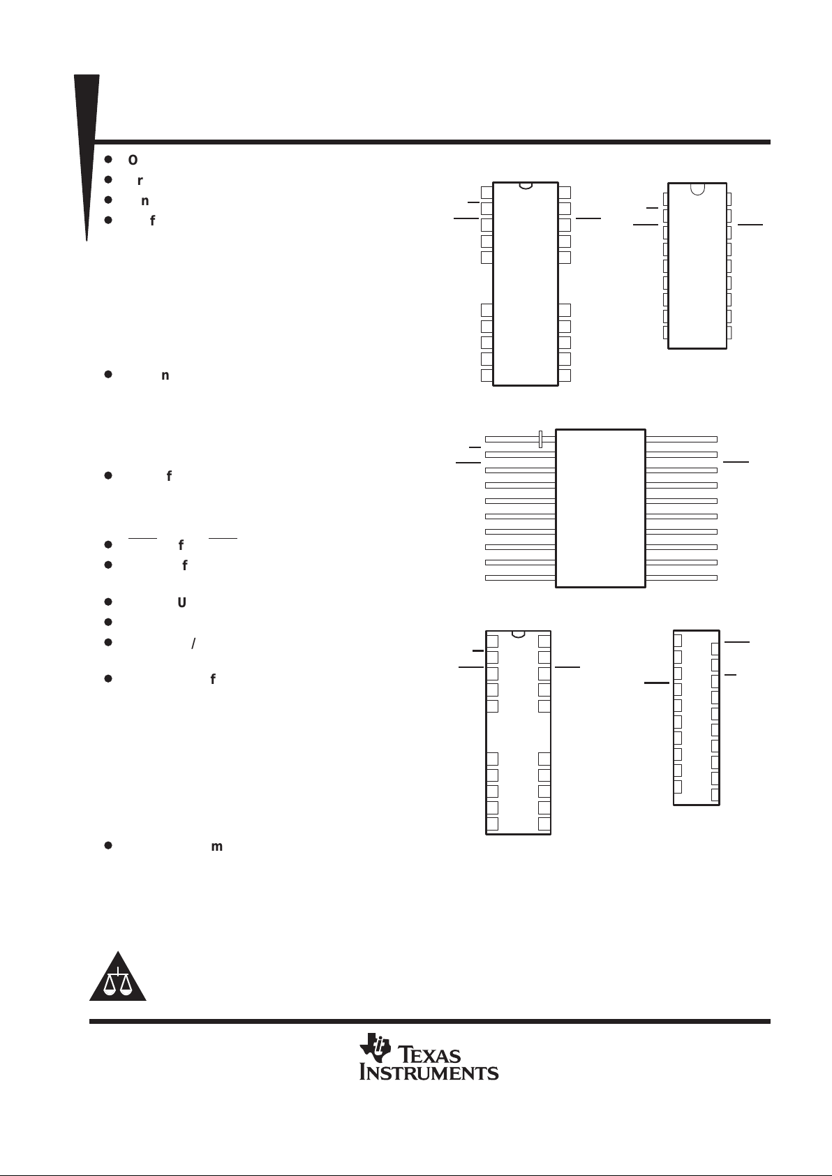
Packaging Offered:
– 20/26-Pin J-Leaded Ceramic Surface
Mount Package (HJ Suffix)
– 18-Pin 300-Mil Ceramic Dual-In-Line
Package (JD Suffix)
– 20-Pin Ceramic Flatpack (HK Suffix)
– 20/26-Terminal Leadless Ceramic
Surface Mount Package (FQ/HL Suffixes)
– 20-Pin Ceramic Zig-Zag In-Line Package
(SV Suffix)
D
Operating Temperature Range
– 55°C to 125°C
Please be aware that an important notice concerning availability, standard warranty, and use in critical applications of
Texas Instruments semiconductor products and disclaimers thereto appears at the end of this data sheet.
V
SS
Q
CAS
NC
A9
A8
A7
A6
A5
A4
D
W
RAS
TF
NC
A0
A1
A2
A3
V
CC
V
SS
Q
CAS
NC
A9
A8
A7
A6
A5
A4
20
19
18
17
16
15
14
13
12
11
1
2
3
4
5
6
7
8
9
10
HJ PACKAGE
(TOP VIEW)
1
2
3
4
5
6
7
8
9
18
17
16
15
14
13
12
11
10
D
W
RAS
TF
A0
A1
A2
A3
V
CC
V
SS
Q
CAS
A9
A8
A7
A6
A5
A4
JD PACKAGE
(TOP VIEW)
1
2
3
4
5
6
7
8
9
10
20
19
18
17
16
15
14
13
12
11
D
W
RAS
TF
NC
A0
A1
A2
A3
V
CC
HK PACKAGE
(TOP VIEW)
A9
Q
D
RAS
NC
A0
V
CC
A5
A7
A2
CAS
V
SS
W
TF
NC
A1
A3
A4
A6
A8
1
3
5
7
9
11
13
15
17
19
2
4
6
8
10
12
14
16
18
20
SV PACKAGE
(SIDE VIEW)
FQ/HL PACKAGES
(TOP VIEW)
11
12
13
14
15
16
17
18
19
20
10
9
8
7
6
5
4
3
2
1
D
W
RAS
TF
NC
A0
A1
A2
A3
V
CC
V
SS
Q
CAS
NC
A9
A8
A7
A6
A5
A4
Copyright 1996, Texas Instruments Incorporated
PRODUCTION DATA information is current as of publication date.
Products conform to specifications per the terms of Texas Instruments
standard warranty. Production processing does not necessarily include
testing of all parameters.
SMJ4C1024
1048576 BY 1-BIT
DYNAMIC RANDOM-ACCESS MEMORY
SGMS023E – DECEMBER 1988 – REVISED MARCH 1996
2
POST OFFICE BOX 1443 • HOUSTON, TEXAS 77251–1443
PIN NOMENCLATURE
A0–A9 Address Inputs
CAS
Column Address Strobe
D Data In
NC No Internal Connection
Q Data Out
RAS
Row Address Strobe
TF Test Function
V
CC
5-V Supply
V
SS
Ground
W
Write Enable
description
The SMJ4C1024 is a 1048576-bit DRAM organized as 1048576 words of one bit each. It employs technology
for high performance, reliability, and low power at a low cost.
This device features maximum RAS
access times of 80 ns, 100 ns, 120 ns, and 150 ns. Maximum power
dissipation is as low as 305 mW operating and 16.5 mW standby on 150-ns devices.
I
DD
peaks are typIcally 140 mA and a –1 V input voltage undershoot can be tolerated, minimizing system noise.
All inputs and outputs, including clocks, are compatible with series 54 TTL. All addresses and data-in lines are
latched on-chip to simplify system design. Data out is unlatched to allow greater system flexibility.
The SMJ4C1024 is offered in an 18-pin ceramic dual-in-line package (JD suffix), a 20/26-terminal leadless
ceramic carrier package (FQ/HL suffixes), a 20/26-pin J-leaded carrier package (HJ suffix), a 20-pin flatpack
(HK suffix), and a 20-pin ceramic zig-zag in-line package (SV suffix). They are characterized for operation from
– 55°C to 125°C.
SMJ4C1024
1048576 BY 1-BIT
DYNAMIC RANDOM-ACCESS MEMORY
SGMS023E – DECEMBER 1988 – REVISED MARCH 1996
3
POST OFFICE BOX 1443 • HOUSTON, TEXAS 77251–1443
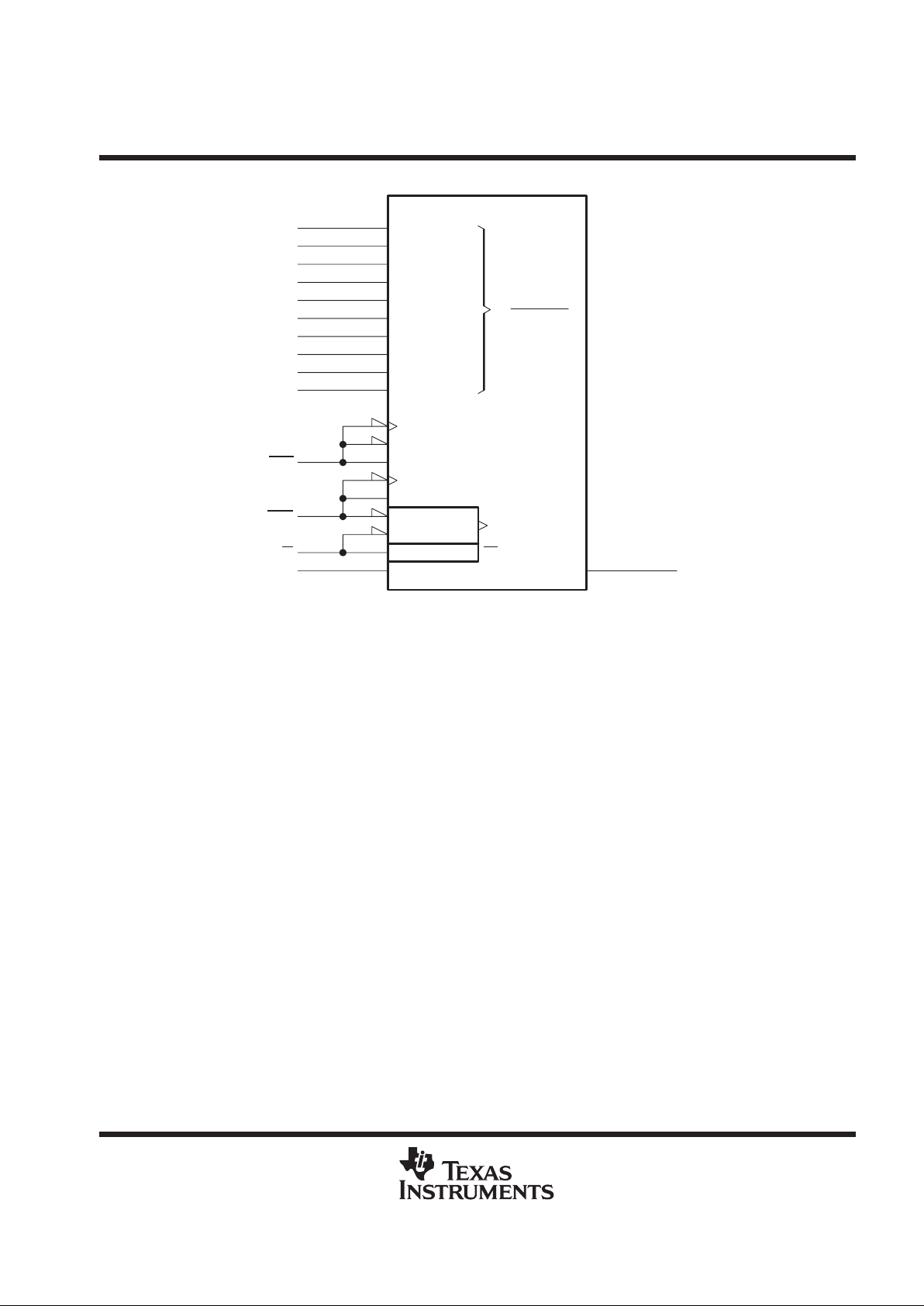
logic symbol
†
A0
A1
A2
A3
A4
A5
A6
A7
A8
RAS
CAS
W
D
5
6
7
8
10
11
12
13
14
3
16
2
1
20D10/21D0
20D19/21D9
C20 [ROW]
G23 [REFRESH ROW]
24 [PWR DWN]
C21 [COL]
G24
23C22
23,21D 24
EN
A, 22D
A
0
1 048 575
RAM 1024K × 1
&
A∇ Q
17
A9
15
†
This symbol is in accordance with ANSI/IEEE Std. 91-1984 and IEC Publication 617-12.
The pin numbers shown are for the 18-pin JD package.
SMJ4C1024
1048576 BY 1-BIT
DYNAMIC RANDOM-ACCESS MEMORY
SGMS023E – DECEMBER 1988 – REVISED MARCH 1996
4
POST OFFICE BOX 1443 • HOUSTON, TEXAS 77251–1443
functional block diagram
RAS CAS W
Timing and Control
Row
Address
Buffers
(10)
Column
Address
Buffers
(10)
A0
A1
A2
A3
A4
A5
A6
A7
A8
A9
256K
Array
Row
Decode
256K
Array
Sense Amplifiers
Sense Amplifiers
256K
Array
Row
Decode
256K
Array
Column Decode
I/O
Buffers
1 of 8
Selection
Data In
Reg.
Data
Out Reg.
D
Q
operation
enhanced page mode
Enhanced page-mode operation allows faster memory access by keeping the same row address while selecting
random column addresses. The time for row-address setup and hold and for address multiplexing is eliminated.
The maximum number of columns that can be accessed is determined by the maximum RAS
low time and the
CAS
page-cycle time used. With minimum CAS page-cycle time, all 1 024 columns specified by column
addresses A0 through A9 can be accessed without intervening RAS
cycles.
Unlike conventional page-mode DRAMs, the column-address buffers in this device are activated on the falling
edge of RAS
. The buffers act as transparent or flow-through latches while CAS is high. The falling edge of CAS
latches the column addresses. This feature lets the SMJ4C1024 operate at a higher data bandwidth than
conventional page-mode parts, since data retrieval begins as soon as the column address is valid rather than
when CAS
goes low. This performance improvement is referred to as enhanced page mode. A valid column
address can be presented immediately after the row-address hold time has been satisfied, usually well in
advance of the falling edge of CAS
. In this case, data is obtained after t
a(C)
maximum (access time from CAS
low) if t
a(CA)
maximum (access time from column address) has been satisfied. If the column addresses for the
next page cycle are valid at the same time CAS
goes high, access time for the next cycle is determined by the
later occurrence of t
a(CA)
or t
a(CP)
(access time from rising edge of CAS).
address (A0–A9)
Twenty address bits are required to decode one of 1048576 storage cell locations. Ten row-address bits are
set up on inputs A0 through A9 and latched onto the chip by RAS
. The ten column-address bits are set up on
pins A0 through A9 and latched onto the chip by CAS
. All addresses must be stable on or before the falling edges

SMJ4C1024
1048576 BY 1-BIT
DYNAMIC RANDOM-ACCESS MEMORY
SGMS023E – DECEMBER 1988 – REVISED MARCH 1996
5
POST OFFICE BOX 1443 • HOUSTON, TEXAS 77251–1443
address (A0–A9) (continued)
of RAS
and CAS. RAS is similar to a chip enable in that it activates the sense amplifiers as well as the row
decoder. CAS
is used as a chip select to activate the output buffer as well as to latch the address bits into the
column-address buffer.
write enable (W
)
The read or write mode is selected through W
. A logic high on the W input selects the read mode and a logic
low selects the write mode. The write-enable pin can be driven from standard TTL circuits without a pullup
resistor. The data input is disabled when the read mode is selected. When W
goes low prior to CAS (early write),
data out remains in the high-impedance state for the entire cycle, permitting common input/output operation.
data in (D)
Data-in is written during a write or a read-modify-write cycle. Depending on the mode of operation, the falling
edge of CAS
or W strobes data into the on-chip latch. In an early-write cycle, W is brought low prior to CAS,
and the data is strobed in by CAS
with setup and hold times referenced to this signal. In a delayed-write or a
read-modify-write cycle, CAS
is already low, and the data is strobed in by W with setup and hold times
referenced to this signal.
data out (Q)
The 3-state output buffers provide direct TTL compatibility (no pullup resistor required) with a fanout of two
series 54 TTL loads. Data out is the same polarity as data in. The output is in the high-impedance (floating) state
until CAS
is brought low. In a read cycle, the output becomes valid after the access time t
a(C)
. The access time
from CAS
low (t
a(C)
) begins with the negative transition of CAS as long as t
a(R)
and t
a(CA)
are satisfied. The output
becomes valid after the access time has elapsed and remains valid while CAS
is low; when CAS goes high, the
output returns to a high-impedance state. In a delayed-write or read-modify-write cycle, the output follows the
sequence for the read cycle.
refresh
A refresh operation must be performed at least once every 8 ms to retain data. This can be achieved by strobing
each of the 512 rows (A0–A8). A normal read or write cycle refreshes all bits in each selected row. A RAS
-only
operation can be used by holding CAS
at the high (inactive) level, conserving power as the output buffer remains
in the high-impedance state. Externally generated addresses must be used for a RAS
-only refresh. Hidden
refresh can be performed while maintaining valid data at the output pin. This is accomplished by holding CAS
at VIL after a read operation and cycling RAS after a specified precharge period, similar to a RAS-only refresh
cycle.
CAS
-before-RAS (CBR) refresh
CBR refresh is used by bringing CAS
low earlier than RAS (see parameter t
d(CLRL)R
) and holding it low after
RAS
falls (parameter t
d(RLCH)R
). For successive CBR refresh cycles, CAS can remain low while cycling RAS.
The external address is ignored and the refresh address is generated internally . The external address is also
ignored during the hidden refresh cycles.
power up
T o achieve proper device operation, an initial pause of 200 µs followed by a minimum of eight initialization cycles
is required after full V
CC
level is achieved.
test function (TF) pin
During normal device operation, TF must be disconnected or biased at a voltage ≤ V
CC
.
SMJ4C1024
1048576 BY 1-BIT
DYNAMIC RANDOM-ACCESS MEMORY
SGMS023E – DECEMBER 1988 – REVISED MARCH 1996
6
POST OFFICE BOX 1443 • HOUSTON, TEXAS 77251–1443
absolute maximum ratings over operating free-air temperature range (unless otherwise noted)
†
Voltage range on any pin (see Note 1) – 1 V to 7 V. . . . . . . . . . . . . . . . . . . . . . . . . . . . . . . . . . . . . . . . . . . . . . . . .
Voltage range on V
CC
– 1 V to 7 V. . . . . . . . . . . . . . . . . . . . . . . . . . . . . . . . . . . . . . . . . . . . . . . . . . . . . . . . . . . . . . . .
Short-circuit output current, I
OS
50 mA. . . . . . . . . . . . . . . . . . . . . . . . . . . . . . . . . . . . . . . . . . . . . . . . . . . . . . . . . . . .
Power dissipation 1 W. . . . . . . . . . . . . . . . . . . . . . . . . . . . . . . . . . . . . . . . . . . . . . . . . . . . . . . . . . . . . . . . . . . . . . . . . .
Operating free-air temperature range, T
A
– 55°C to 125°C. . . . . . . . . . . . . . . . . . . . . . . . . . . . . . . . . . . . . . . . . .
Storage temperature range, T
stg
–65°C to 150°C. . . . . . . . . . . . . . . . . . . . . . . . . . . . . . . . . . . . . . . . . . . . . . . . . .
†
Stresses beyond those listed under “absolute maximum ratings” may cause permanent damage to the device. These are stress ratings only, and
functional operation of the device at these or any other conditions beyond those indicated under “recommended operating conditions” is not
implied. Exposure to absolute-maximum-rated conditions for extended periods may affect device reliability.
NOTE 1: All voltage values are with respect to VSS.
recommended operating conditions
MIN NOM MAX UNIT
V
CC
Supply voltage 4.5 5 5.5 V
V
IH
High-level input voltage 2.4 6.5 V
V
IL
Low-level input voltage (see Note 2) –1 0.8 V
T
A
Minimum operating free-air temperature – 55
°C
T
C
Maximum operating case temperature 125
°C
NOTE 2: The algebraic convention, where the more negative (less positive) limit is designated as minimum, is used for logic-voltage levels only.
SMJ4C1024
1048576 BY 1-BIT
DYNAMIC RANDOM-ACCESS MEMORY
SGMS023E – DECEMBER 1988 – REVISED MARCH 1996
7
POST OFFICE BOX 1443 • HOUSTON, TEXAS 77251–1443
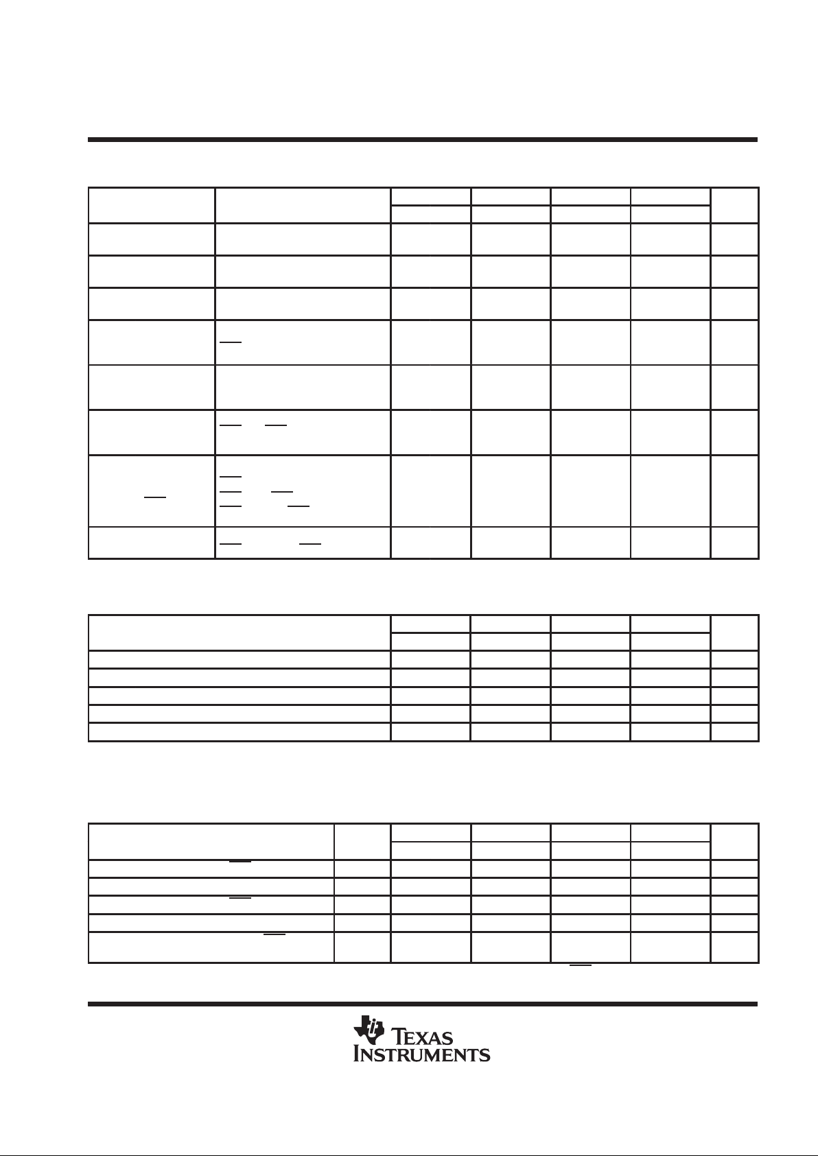
electrical characteristics over recommended ranges of supply voltage and operating free-air
temperature (unless otherwise noted)
TEST
’4C1024-80 ’4C1024-10 ’4C1024-12 ’4C1024-15
PARAMETER
CONDITIONS
MIN MAX MIN MAX MIN MAX MIN MAX
UNIT
V
OH
High-level
output voltage
IOH = – 5 mA 2.4 2.4 2.4 2.4 V
V
OL
Low-level
output voltage
IOL = 4.2 mA 0.4 0.4 0.4 0.4 V
I
I
Input current
(leakage)
VCC = 5.5 V, VI = 0 V to 6.5 V,
All other pins = 0 V to V
CC
± 10 ± 10 ± 10 ± 10 µA
I
O
Output
current
(leakage)
VCC = 5.5 V, VO = 0 V to VCC,
CAS
high
± 10 ± 10 ± 10 ± 10 µA
I
CC1
Read- or
write-cycle
current
VCC = 5.5 V, Minimum cycle 75 70 60 55 mA
I
CC2
Standby
current
After one memory cycle,
RAS
and CAS high,
VIH = 2.4 V
3 3 3 3 mA
I
CC3
Average
refresh
current
(RAS
only or
CBR)
VCC = 5.5 V, Minimum cycle,
RAS
cycling,
CAS
high (RAS only),
RAS
low after CAS low (CBR)
70 65 55 50 mA
I
CC4
Average page
current
VCC = 5.5 V, tPC = minimum,
RAS
low, CAS cycling
50 45 35 30 mA
capacitance over recommended ranges of supply voltage and operating free-air temperature,
f = 1 MHz (see Note 3)
HL/JD/FQ HJ HK SV
PARAMETER
MIN MAX MIN MAX MIN MAX MIN MAX
UNIT
C
i(A)
Input capacitance, address inputs 6 7 8 9 pF
C
i(D)
Input capacitance, data input 5 5 6 7 pF
C
i(RC)
Input capacitance, strobe inputs 7 7 8 8 pF
C
i(W)
Input capacitance, write-enable input 7 7 7 7 pF
C
o
Output capacitance 7 9 10 8 pF
NOTE 3: Capacitance is sampled only at initial design and after any major change. Samples are tested at 0 V and 25°C with a 1-MHz signal
applied to the pin under test. All other pins are open.
switching characteristics over recommended ranges of supply voltage and operating free-air
temperature (see Figure 1)
ALT.
’4C1024-80 ’4C1024-10 ’4C1024-12 ’4C1024-15
PARAMETER
SYMBOL
MIN MAX MIN MAX MIN MAX MIN MAX
UNIT
t
a(C)
Access time from CAS low t
CAC
20 25 30 40 ns
t
a(CA)
Access time from column address t
AA
40 45 55 70 ns
t
a(R)
Access time from RAS low t
RAC
80 100 120 150 ns
t
a(CP)
Access time from column precharge t
CPA
40 40 60 75 ns
t
dis(CH)
Output disable time after CAS high
(see Note 4)
t
OFF
20 25 30 35 ns
NOTE 4: t
dis(CH)
is specified when the output is no longer driven. The output is disabled by bringing CAS high.
SMJ4C1024
1048576 BY 1-BIT
DYNAMIC RANDOM-ACCESS MEMORY
SGMS023E – DECEMBER 1988 – REVISED MARCH 1996
8
POST OFFICE BOX 1443 • HOUSTON, TEXAS 77251–1443
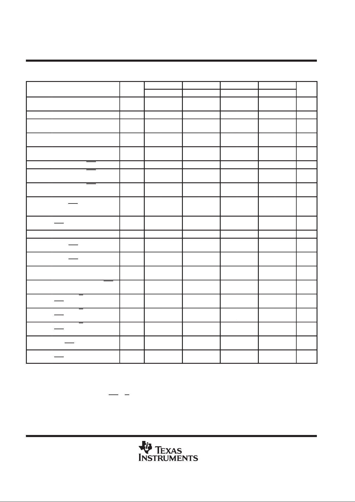
timing requirements over recommended ranges of supply voltage and operating free-air
temperature (see Note 5)
ALT.
’4C1024-80 ’4C1024-10 ’4C1024-12 ’4C1024-15
SYMBOL
MIN MAX MIN MAX MIN MAX MIN MAX
UNIT
t
c(rd)
Cycle time, read
(see Note 6)
t
RC
150 190 220 260 ns
t
c(W)
Cycle time, write t
WC
150 190 220 260 ns
t
c(rdW)
Cycle time,
read-write/read-modify-write
t
RWC
175 220 265 315 ns
t
c(P)
Cycle time, page-mode read
or write (see Note 7)
t
PC
50 55 65 80 ns
t
c(PM)
Cycle time, page-mode
read-modify-write
t
PRWC
75 85 110 135 ns
t
w(CH)
Pulse duration, CAS high t
CP
10 10 15 25 ns
t
w(CL)
Pulse duration, CAS low
(see Note 8)
t
CAS
20 10000 25 10000 30 10000 40 10000 ns
t
w(RH)
Pulse duration, RAS high
(precharge)
t
RP
60 80 90 100 ns
t
w(RL)
Pulse duration, nonpage
mode, RAS
low
(see Note 9)
t
RAS
80 10000 100 10000 120 10000 150 10000 ns
t
w(RL)P
Pulse duration, page mode,
RAS
low (see Note 9)
t
RASP
80 100000 100 100000 120 100000 150 100000 ns
t
w(WL)
Pulse duration, write t
WP
15 15 20 25 ns
t
su(CA)
Setup time, column address
before CAS
low
t
ASC
0 3 3 3 ns
t
su(RA)
Setup time, row address
before RAS
low
t
ASR
0 0 0 0 ns
t
su(D)
Setup time, data
(see Note 10)
t
DS
0 0 0 0 ns
t
su(rd)
Setup time, read before CAS
low
t
RCS
0 0 0 0 ns
t
su(WCL)
Setup time, W low before
CAS
low (see Note 11)
t
WCS
0 0 0 0 ns
t
su(WCH)
Setup time, W low before
CAS
high
t
CWL
20 25 30 40 ns
t
su(WRH)
Setup time, W low before
RAS
high
t
RWL
20 25 30 40 ns
t
h(CA)
Hold time, column address
after CAS
low
t
CAH
15 20 20 25 ns
t
h(RA)
Hold time, row address after
RAS
low
t
RAH
12 15 15 20 ns
NOTES: 5. Timing measurements in this table are referenced to VIL max and VIH min.
6. All cycle times assume tt = 5 ns.
7. To assure t
c(P)
min, t
su(CA)
should be ≥ t
w(CH)
.
8. In a read-modify-write cycle, t
d(CLWL)
and t
su(WCH)
must be observed.
9. In a read-modify-write cycle, t
d(RLWL)
and t
su(WRH)
must be observed.
10. Referenced to the later of CAS
or W in write operations
11. Early write operation only

SMJ4C1024
1048576 BY 1-BIT
DYNAMIC RANDOM-ACCESS MEMORY
SGMS023E – DECEMBER 1988 – REVISED MARCH 1996
9
POST OFFICE BOX 1443 • HOUSTON, TEXAS 77251–1443
timing requirements over recommended ranges of supply voltage and operating free-air
temperature (see Note 5) (continued)
ALT.
’4C1024-80 ’4C1024-10 ’4C1024-12 ’4C1024-15
SYMBOL
MIN MAX MIN MAX MIN MAX MIN MAX
UNIT
t
h(RLCA)
Hold time, column address after
RAS
low (see Note 12)
t
AR
60 70 80 100 ns
t
h(D)
Hold time, data (see Note 10) t
DH
15 20 25 30 ns
t
h(RLD)
Hold time, data after RAS low
(see Note 12)
t
DHR
60 70 85 110 ns
t
h(CHrd)
Hold time, read after CAS high
(see Note 13)
t
RCH
0 0 0 0 ns
t
h(RHrd)
Hold time, read after RAS high
(see Note 13)
t
RRH
10 10 10 10 ns
t
h(CLW)
Hold time, write after CAS low
(see Note 11)
t
WCH
15 20 25 30 ns
t
h(RLW)
Hold time, write after RAS low
(see Note 12)
t
WCR
60 70 85 100 ns
t
d(RLCH)
Delay time, RAS low to CAS high t
CSH
80 100 120 150 ns
t
d(CHRL)
Delay time, CAS high to RAS low t
CRP
0 0 0 0 ns
t
d(CLRH)
Delay time, CAS low to RAS high t
RSH
20 25 30 40 ns
t
d(CLWL)
Delay time, CAS low to W low
(see Note 14)
t
CWD
20 25 40 50 ns
t
d(RLCL)
Delay time, RAS low to CAS low
(see Note 15)
t
RCD
22 60 28 75 28 90 33 110 ns
t
d(RLCA)
Delay time, RAS low to column
address (see Note 15)
t
RAD
17 40 20 55 20 65 25 80 ns
t
d(CARH)
Delay time, column address to RAS
high
t
RAL
40 45 55 70 ns
t
d(CACH)
Delay time, column address to CAS
high
t
CAL
40 45 55 70 ns
t
d(RLWL)
Delay time, RAS low to W low
(see Note 14)
t
RWD
80 100 130 160 ns
t
d(CAWL)
Delay time, column address to W
low (see Note 14)
t
AWD
40 45 65 80 ns
t
d(RLCH)R
Delay time, RAS low to CAS high
(see Note 16)
t
CHR
20 25 25 30 ns
t
d(CLRL)R
Delay time, CAS low to RAS low
(see Note 16)
t
CSR
10 10 10 15 ns
t
d(RHCL)R
Delay time, RAS high to CAS low t
RPC
0 0 0 0 ns
t
rf
Refresh time interval t
REF
8 8 8 8 ms
t
t
Transition time (see Note 17) — — — — — ns
NOTES: 5. Timing measurements in this table are referenced to VIL max and VIH min.
10. Referenced to the later of CAS
or W in write operations.
11. Early-write operation only
12. The minimum value is measured when t
d(RLCL)
is set t
d(RLCL)
min as a reference.
13. Either t
h(RHrd)
or t
h(CHrd)
must be satisfied for a read cycle.
14. Read-modify-write operation only
15. Maximum value specified only to assure access time.
16. CBR refresh only
17. Transition times (rise and fall) for RAS
and CAS are to be minimum of 3 ns and a maximum of 50 ns.
 Loading...