

AUSTIN SMJ44C256-10, SMJ44C256-12, SMJ44C256-14, SMJ44C256-80 Datasheet
DQ1
DQ2
W
RAS
TF
A0
A1
A2
A3
V
CC
V
SS
DQ4
DQ3
CAS
G
A8
A7
A6
A5
A4
20
19
18
17
16
15
14
13
12
11
1
2
3
4
5
6
7
8
9
10
JD PACKAGE
(TOP VIEW)
G
DQ3
V
SS
DQ2
RAS
A0
A2
V
CC
A5
A7
CAS
DQ4
DQ1
W
TF
A1
A3
A4
A6
A8
2
4
6
8
10
12
14
16
18
20
1
3
5
7
9
11
13
15
17
19
SV PACKAGE
(TOP VIEW)
RAS
A0
A1
A2
A3
V
CC
A8
A7
A6
A5
A4
V
SS
DQ4
DQ3
CAS
G
HJ PACKAGE
(TOP VIEW)
DQ1
DQ2
W
TF
26
25
24
23
22
18
17
16
15
14
1
2
3
4
5
9
10
11
12
13
FQ/HL PACKAGES
(TOP VIEW)
V
SS
DQ4
DQ3
CAS
G
A8
A7
A6
A5
A4
1
2
3
4
5
6
7
8
9
10
20
19
18
17
16
15
14
13
12
11
DQ1
DQ2
W
RAS
TF
A0
A1
A2
A3
V
CC
HK PACKAGE
(TOP VIEW)
RAS
A0
A1
A2
A3
V
CC
A8
A7
A6
A5
A4
V
SS
DQ4
DQ3
CAS
G
DQ1
DQ2
W
TF
26
25
24
23
22
18
17
16
15
14
1
2
3
4
5
9
10
11
12
13
SMJ44C256
262144 BY 4-BIT
DYNAMIC RANDOM-ACCESS MEMORY
SGMS034C – MAY 1989 – REVISED JUNE 1995
1
POST OFFICE BOX 1443 • HOUSTON, TEXAS 77251–1443
D
Organization...262144 Words × 4 Bits
D
Single 5-V Supply (10% Tolerance)
D
Processed to MIL-STD-833, Class B
D
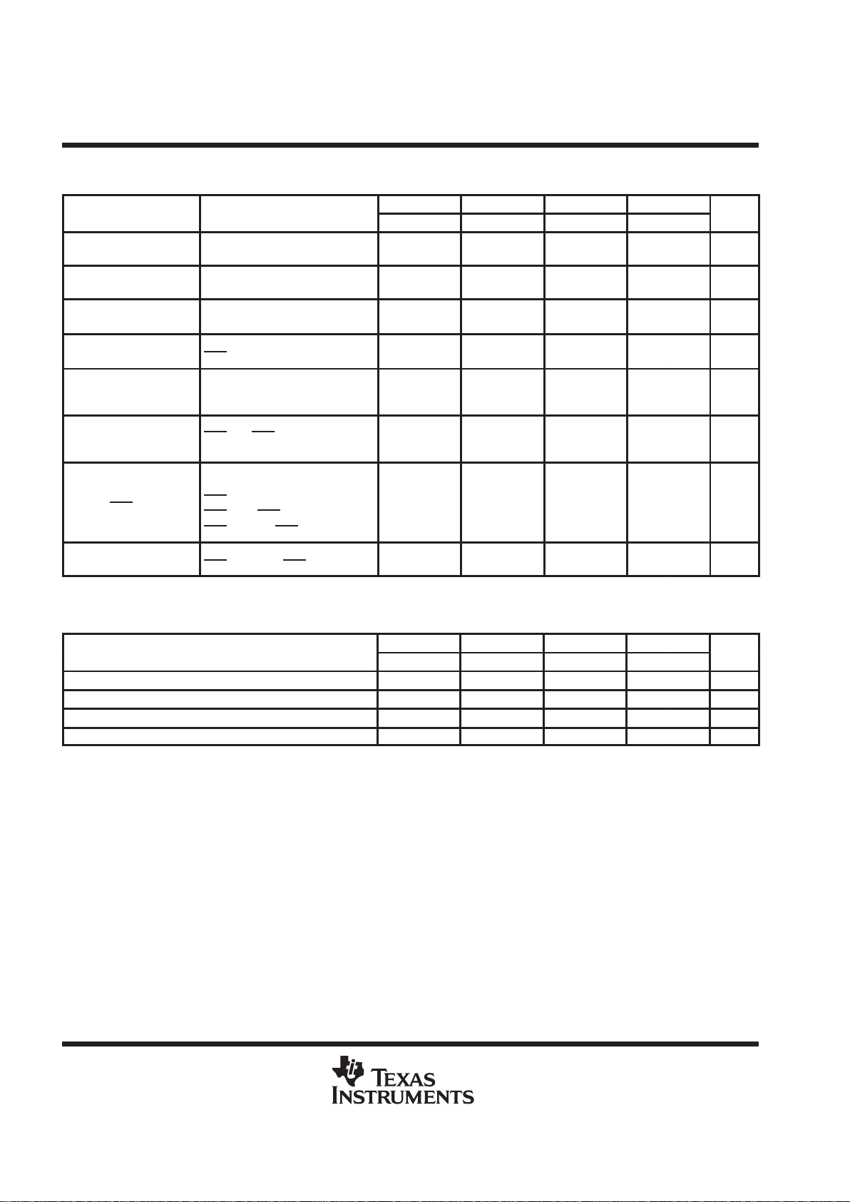
Performance Ranges:
ACCESS ACCESS ACCESS READ
TIME TIME TIME OR
t
a(R)
t
a(C)
t
a(CA)
WRITE
(t
RAC
)(t
CAC
)(t
CAA
) CYCLE
(MAX) (MAX) (MAX) (MIN)
SMJ44C256-80 80 ns 20 ns 40 ns 150 ns
SMJ44C256-10 100 ns 25 ns 45 ns 190 ns
SMJ44C256-12 120 ns 30 ns 55 ns 220 ns
SMJ44C256-15 150 ns 40 ns 70 ns 260 ns
D
Enhanced Page-Mode Operation With
CAS
-Before-RAS (CBR) Refresh
D
Long Refresh Period
512-Cycle Refresh in 8 ms (Max)
D
All Inputs and Clocks are TTL Compatible
D
3-State Unlatched Output
D
Low Power Dissipation
D
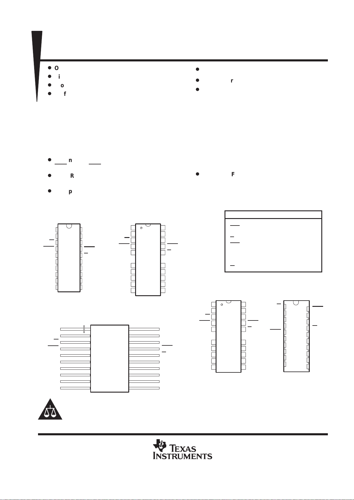
Packaging Offered:
– 20-Pin 300-Mil Ceramic DIP (JD Suffix)
– 20-Lead Ceramic Surface-Mount Package
(HJ Suffix)
– 20-Pin Ceramic Flat Pack (HK Suffix)
– 20-Terminal Leadless Ceramic
Surface-Mount Package (FQ Suffix)
– 20-Terminal Low-Profile Leadless
Ceramic Surface-Mount Package
(HL Suffix)
– 20-Pin Ceramic Zig Zag In-Line Package
(SV Suffix)
D
Operating Free-Air Temperature Range
– 55°C to 125°C
PIN NOMENCLATURE
A0–A8
CAS
DQ1–DQ4
G
RAS
TF
V
CC
V
SS
W
Address Inputs
Column Address Strobe
Data In/Data Out
Data Output Enable
Row Address Strobe
Test Function
5-V Supply
Ground
Write Enable
Copyright 1995, Texas Instruments Incorporated
PRODUCTION DATA information is current as of publication date.
Products conform to specifications per the terms of Texas Instruments
standard warranty. Production processing does not necessarily include
testing of all parameters.
Please be aware that an important notice concerning availability, standard warranty, and use in critical applications of
Texas Instruments semiconductor products and disclaimers thereto appears at the end of this data sheet.
SMJ44C256
262144 BY 4-BIT
DYNAMIC RANDOM-ACCESS MEMORY
SGMS034C – MAY 1989 – REVISED JUNE 1995
2
POST OFFICE BOX 1443 • HOUSTON, TEXAS 77251–1443
description
The SMJ44C256 series is a set of high-speed, 1 048 576-bit dynamic random access memories (DRAMs),
organized as 262 144 words of four bits each. These devices employ technology for high performance,
reliability, and low power.
These devices feature maximum RAS
access times of 80 ns, 100 ns,120 ns, and 150 ns. Maximum power
dissipation is as low as 305 mW operating and 16.5 mW standby on 150-ns devices.
I
CC
peaks are 140 mA typical, and an input voltage undershoot of –1 V can be tolerated, minimizing system noise
considerations.
All inputs and outputs, including clocks, are compatible with Series 54/174 TTL. All addresses and data-in lines
are latched on-chip to simplify system design. Data out is unlatched to allow greater system flexibility.
The SMJ44C256 is offered in 20-pin ceramic dual-in-line packages (JD suffix) and 20/26-terminal ceramic
leadless carriers (FQ /HL suffixes), 20/26-pin leaded carrier (HJ suffix), a 20-pin flatpack (HK suffix), and a
20-pin ceramic zig-zag in-line package (SV suffix). They are specified for operation from –55°C to125°C.
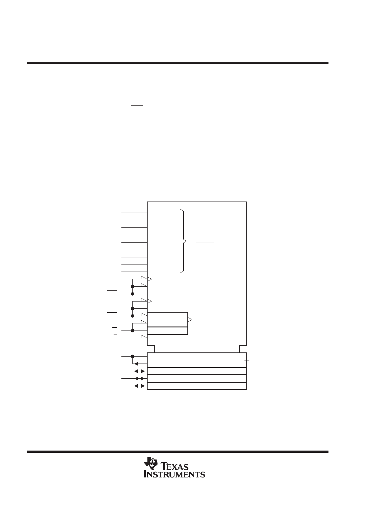
logic symbol
†
A0
A1
A2
A3
A4
A5
A6
A7
A8
RAS
CAS
W
G
DQ1
DQ3
DQ2
DQ4
6
7
8
9
11
12
13
14
15
4
17
3
16
1
2
18
19
20D9/21D0
20D17/21D8
C20[ROW]
G23/[REFRESH ROW]
24[PWR DWN]
C21/[COLUMN]
G24
&
23,21D
G25
A,22D
∇ 26
24,25EN
23C22
A,Z26
RAM 256K × 4
A
0
262 143
†
This symbol is in accordance with ANSI/IEEE Std 91-1984 and IEC Publication 617-12. Pin numbers shown are for the JD package.
SMJ44C256
262144 BY 4-BIT
DYNAMIC RANDOM-ACCESS MEMORY
SGMS034C – MAY 1989 – REVISED JUNE 1995
3
POST OFFICE BOX 1443 • HOUSTON, TEXAS 77251–1443
functional block diagram
Row
Address
Buffers
(9)
Column
Address
Buffers
(9)
A0
A1
A2
A3
A4
A5
A6
A7
A8
256K
Array
Row
Decode
256K
Array
256K
Array
Row
Decode
256K
Array
Column Decode
I/O
Buffers
4 of 8
Selection
Data
In
Reg
Data
Out
Reg
DQ1–DQ4
4
4
4
RAS
CAS W G
Sense Amplifiers
Sense Amplifiers
Timing and Control
operation
enhanced page mode
Page-mode operation allows faster memory access by keeping the same row address while selecting random
column addresses. The time for row-address setup and hold and address multiplex is eliminated. The maximum
number of columns that can be accessed is determined by the maximum RAS
low time and the CAS page cycle
time used. With minimum CAS
page cycle time, all 512 columns specified by column addresses A0 through A8
can be accessed without intervening RAS
cycles.
Unlike conventional page mode DRAMs, the column-address buffers in this device are activated on the falling
edge of RAS
. The buffers act as transparent or flow-through latches while CAS is high. The column address
latches to the first CAS
falling edge. This feature allows the SMJ44C256 to operate at a wider data bandwidth
than conventional page mode parts, since data retrieval begins as soon as column address is valid rather than
when CAS
goes low. This performance improvement is referred to as enhanced page mode. Valid column
address can be presented immediately after t
h(RA)
(row address hold time) has been satisfied, usually well in
advance of the falling edge of CAS
. In this case, data is obtained after t
a(C)
maximum (access time from CAS
low), if t
a(CA)
maximum (access time from column address) has been satisfied. In the event that column
addresses for the next page cycle are valid at the time CAS
goes high, access time for the next cycle is
determined by the later occurrence of t
a(C)
or t
a(CP)
(access time from rising edge of CAS).

SMJ44C256
262144 BY 4-BIT
DYNAMIC RANDOM-ACCESS MEMORY
SGMS034C – MAY 1989 – REVISED JUNE 1995
4
POST OFFICE BOX 1443 • HOUSTON, TEXAS 77251–1443
address (A0 through A8)
Eighteen address bits are required to decode 1 of 262144 storage cell locations. Nine row-address bits are set
up on pins A0 through A8 and latched onto the chip by RAS. Nine column-address bits are set up on pins A0
through A8 and latched onto the chip by CAS
. All addresses must be stable on or before the falling edges of
RAS
and CAS. RAS is similar to a chip enable in that it activates the sense amplifiers as well as the row decoder.
In the SMJ44C256, CAS
is used as a chip select, activating the output buffer as well as latching the address
bits into the column-address buffers.
write enable (W
)
The read or write mode is selected through W
. A logic high on the W input selects the read mode and a logic
low selects the write mode. The write-enable terminal can be driven from the standard TTL circuits without a
pullup resistor. The data input is disabled when the read mode is selected. When W
goes low prior to CAS
(early-write), data out remains in the high-impedance state for the entire cycle, permitting a write operation with
G
grounded.
data in (DQ1–DQ4)
Data is written during a write or read-modify-write cycle. Depending on the mode of operation, the falling edge
of CAS
or W strobes data into the on-chip data latch. In an early-write cycle, W is brought low prior to CAS and
the data is strobed in by CAS
with setup and hold times referenced to this signal. In a delayed-write or
read-modify-write cycle, CAS
is already low, the data is strobed in by W with setup and hold times referenced
to this signal. In a delayed-write or read-modify-write cycle, G
must be high to bring the output buffers to the
high-impedance state prior to applying data to the I/O lines.
data out (DQ1–DQ4)
The 3-state output buffer provides direct TTL compatibility (no pullup resistor required) with a fanout of two
Series 54 TTL loads. Data out is the same polarity as data in. The output is in the high-impedance (floating) state
until CAS
and G are brought low. In a read cycle the output becomes valid after the access time interval t
a(C)
that begins with the negative transition of CAS as long as t
a(R)
and t
a(CA)
are satisfied. The output becomes valid
after the access time has elapsed and remains valid while CAS
and G are low. CAS or G going high returns it
to a high-impedance state. This is accomplished by bringing G
high prior to applying data, thus satisfying t
d(GHD)
.
output enable (G
)
G
controls the impedance of the output buffers. When G is high, the buffers remain in the high-impedance state.
Bringing G
low during a normal cycle activates the output buffers, putting them in the low-impedance state. It
is necessary for both G
and CAS to be brought low for the output buffers, to go into the low-impedance state.
Once in the low-impedance state, they remain in the low-impedance state until either G
or CAS is brought high.
refresh
A refresh operation must be performed at least once every 8 ms to retain data. This can be achieved by strobing
each of the 512 rows (A0–A8). A normal read or write cycle refreshes all bits in each row that is selected. A
RAS
-only operation can be used by holding CAS at the high (inactive) level, conserving power as the output
buffer remains in the high-impedance state. Externally generated addresses must be used for a RAS
-only
refresh. Hidden refresh can be performed while maintaining valid data at the output pin. This is accomplished
by holding CAS
at VIL after a read operation and cycling RAS after a specified precharge period, similar to a
RAS
-only refresh cycle.
CBR refresh
CBR refresh is utilized by bringing CAS
low earlier than RAS [see parameter t
d(CLRL)R
] and holding it low after
RAS
falls [see parameter t
d(RLCH)R
]. For successive CBR refresh cycles, CAS can remain low while cycling
RAS
. The external address is ignored and the refresh address is generated internally . The external address is
also ignored during the hidden refresh option.
SMJ44C256
262144 BY 4-BIT
DYNAMIC RANDOM-ACCESS MEMORY
SGMS034C – MAY 1989 – REVISED JUNE 1995
5
POST OFFICE BOX 1443 • HOUSTON, TEXAS 77251–1443
power up
To achieve proper device operation, an initial pause of 200 µs followed by a minimum of eight initialization
(refresh) cycles is required after power-up to the full V
CC
level.
test function pin
During normal device operation the TF pin must either be disconnected or biased at a voltage less than or equal
to V
CC
.
absolute maximum ratings over operating free-air temperature range (unless otherwise noted)
†
Supply voltage range, V
CC
0 V to 7 V. . . . . . . . . . . . . . . . . . . . . . . . . . . . . . . . . . . . . . . . . . . . . . . . . . . . . . . . . . . . .
Voltage range on any pin (see Note 1) – 1 V to 7 V. . . . . . . . . . . . . . . . . . . . . . . . . . . . . . . . . . . . . . . . . . . . . . . . .
Short-circuit output current 50 mA. . . . . . . . . . . . . . . . . . . . . . . . . . . . . . . . . . . . . . . . . . . . . . . . . . . . . . . . . . . . . . . .
Continuous total power dissipation 1 W. . . . . . . . . . . . . . . . . . . . . . . . . . . . . . . . . . . . . . . . . . . . . . . . . . . . . . . . . . .
Operating free-air temperature range, T
A
– 55°C to 125°C. . . . . . . . . . . . . . . . . . . . . . . . . . . . . . . . . . . . . . . . . .
Storage temperature range, T
stg
–65°C to 150°C. . . . . . . . . . . . . . . . . . . . . . . . . . . . . . . . . . . . . . . . . . . . . . . . . .
†
Stresses beyond those listed under “absolute maximum ratings” may cause permanent damage to the device. These are stress ratings only, and
functional operation of the device at these or any other conditions beyond those indicated under “recommended operating conditions” is not
implied. Exposure to absolute-maximum-rated conditions for extended periods may affect device reliability.
NOTE 1: All voltage values are with respect to VSS.
recommended operating conditions
MIN NOM MAX UNIT
V
CC
Supply voltage 4.5 5 5.5 V
V
SS
Supply voltage 0 V
V
IH
High-level input voltage 2.4 6.5 V
V
IL
Low-level input voltage (see Note 2) –1 0.8 V
T
A
Operating free-air temperature –55
°C
T
C
Case temperature 125
°C
NOTE 2: The algebraic convention, where the more negative (less positive) limit is designated as minimum, is used for logic-voltage levels only.
SMJ44C256
262144 BY 4-BIT
DYNAMIC RANDOM-ACCESS MEMORY
SGMS034C – MAY 1989 – REVISED JUNE 1995
6
POST OFFICE BOX 1443 • HOUSTON, TEXAS 77251–1443
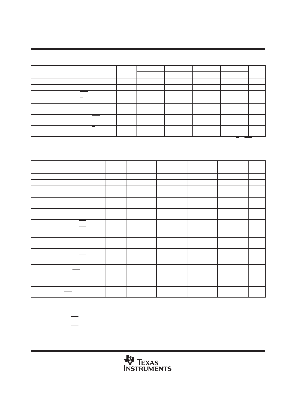
electrical characteristics over recommended ranges of supply voltage and operating free-air
temperature (unless otherwise noted)
’44C256-80 ’44C256-10 ’44C256-12 ’44C256-15
PARAMETER
TEST CONDITIONS
MIN MAX MIN MAX MIN MAX MIN MAX
UNIT
V
OH
High-level output
voltage
IOH = – 5 mA 2.4 2.4 2.4 2.4 V
V
OL
Low-level output
voltage
IOL = 4.2 mA 0.4 0.4 0.4 0.4 V
I
I
Input current
(leakage)
VCC = 5 V, VI = 0 V to 6.5 V,
All other pins = 0 V to V
CC
± 10 ± 10 ± 10 ± 10 µA
I
O
Output current
(leakage)
VCC = 5.5 V, VO = 0 to VCC,
CAS
high
± 10 ± 10 ± 10 ± 10 µA
I
CC1
Read- or
write-cycle
current
VCC = 5.5 V,
t
c(rdW)
= minimum
80 70 60 55 mA
I
CC2
Standby current
After 1 memory cycle,
RAS
and CAS high,
VIH = 2.4 V
3 3 3 3 mA
I
CC3
Average refresh
current
(RAS
only, or
CBR)
VCC = 5.5 V,
t
c(rdW)
= minimum,
RAS
cycling,
CAS
high (RAS only),
RAS
low after CAS low (CBR)
75 65 55 50 mA
I
CC4
Average page
current
VCC = 5.5 V, t
c(P)
= minimum,
RAS
low, CAS cycling
50 45 35 30 mA
capacitance over recommended ranges of supply voltage and operating free-air temperature,
f = 1 MHz (see Note 3)
HL /JD/FQ HJ HK SV
PARAMETER
MIN MAX MIN MAX MIN MAX MIN MAX
UNIT
C
i(A)
Input capacitance, address inputs 6 7 8 9 pF
C
i(RC)
Input capacitance, strobe inputs 7 7 8 8 pF
C
i(W)
Input capacitance, write-enable input 7 7 7 7 pF
C
O
Output capacitance 7 9 10 8 pF
NOTE 3: Capacitance is sampled only at initial design and after any major change. Samples are tested at 0 V and 25°C with a 1-MHz signal
applied to the pin under test. All other pins are open.
SMJ44C256
262144 BY 4-BIT
DYNAMIC RANDOM-ACCESS MEMORY
SGMS034C – MAY 1989 – REVISED JUNE 1995
7
POST OFFICE BOX 1443 • HOUSTON, TEXAS 77251–1443
switching characteristics over recommended ranges of supply voltage and operating free-air
temperature (see Figure 1)
ALT.
’44C256-80 ’44C256-10 ’44C256-12 ’44C256-15
PARAMETER
SYMBOL
MIN MAX MIN MAX MIN MAX MIN MAX
UNIT
t
a(C)
Access time from CAS low t
CAC
20 25 30 40 ns
t
a(CA)
Access time from column-address t
AA
40 45 55 70 ns
t
a(RL)
Access time from RAS low t
RAC
80 100 120 150 ns
t
a(G)
Access time from G low t
GAC
20 25 30 40 ns
t
a(CP)
Access time from CAS high column
precharge
t
CPA
40 50 60 75 ns
t
dis(CH)
Output disable time after CAS high
(see Note 4)
t
OFF
20 25 30 35 ns
t
dis(G)
Output disable time after G high
(see Note 4)
t
GOFF
20 25 30 35 ns
NOTE 4: t
dis(CH)
and t
dis(G)
are specified when the output is no longer driven. The outputs are disabled by bringing either G or CAS high.
timing requirements over recommended ranges of supply voltage and operating free-air
temperature (see Note 5)
ALT.
’44C256-80 ’44C256-10 ’44C256-12 ’44C256-15
PARAMETER
SYMBOL
MIN MAX MIN MAX MIN MAX MIN MAX
UNIT
t
c(rd)
Cycle time, read (see Note 6) t
RC
150 190 220 260 ns
t
c(W)
Cycle time, write t
WC
150 190 220 260 ns
t
c(rdW)
Cycle time,read-write/readmodify-write
t
RWC
225 270 305 355 ns
t
c(P)
Cycle time, page-mode read
or write (see Note 7)
t
PC
50 55 65 80 ns
t
c(PM)
Cycle time, page-mode readmodify-write
t
PRWC
115 135 150 175 ns
t
w(CH)
Pulse duration, CAS high t
CP
10 10 15 25 ns
t
w(CL)
Pulse duration, CAS low
(see Note 8)
t
CAS
20 10 000 25 10 000 30 10 000 40 10 000 ns
t
w(RH)
Pulse duration, RAS high
(precharge)
t
RP
60 80 90 100 ns
t
w(RL)
Pulse duration,
nonpage mode RAS
low
(see Note 9)
t
RAS
80 10 000 100 10 000 120 10 000 150 10 000 ns
t
w(RL)P
Pulse duration,
page mode RAS
low
(see Note 9)
t
RASP
80 100 000 100 100 000 120 100 000 150 100 000 ns
t
w(WL)
Pulse duration, write low t
WP
15 15 20 25 ns
t
su(CA)
Setup time, column address
before CAS
low
t
ASC
5 5 5 5 ns
NOTES: 5. Timing measurements in this table are referenced to VIL max and VIH min.
6. All cycle times assume tt = 5 ns.
7. To assure t
c(P)
min, t
su(CA)
should be ≥ t
w(CH)
.
8. In a read-modify-write cycle, t
d(CLWL)
and t
su(WCH)
must be observed. Depending on the user’s transition times, this can require
additional CAS
low time [t
w(CL)
].
9. In a read-modify-write cycle, t
d(RLWL)
and t
su(WRH)
must be observed. Depending on the user’s transition times, this can require
additional RAS
low time [t
w(RL)
].
 Loading...