

AUSTIN SMJ44400-80JDM, SMJ44C251B, SMJ44400-10HRM, SMJ44400-10JDM, SMJ44400-12HRM Datasheet
...
DRAM
SMJ44400
Austin Semiconductor, Inc.
SMJ44400
Rev. 2.0 10/01
Austin Semiconductor, Inc. reserves the right to change products or specifications without notice.
1
FEATURES
• Organized 1,048,576 x 4
OPTIONS MARKING
• Timing
80ns access -8 0
100ns access -1 0
120ns access -1 2
• Package(s)
Ceramic DIP (400mils) JD No. 113
Ceramic Flatpack HR No. 308
• Operating Temperature Ranges
Military (-55oC to +125oC) M
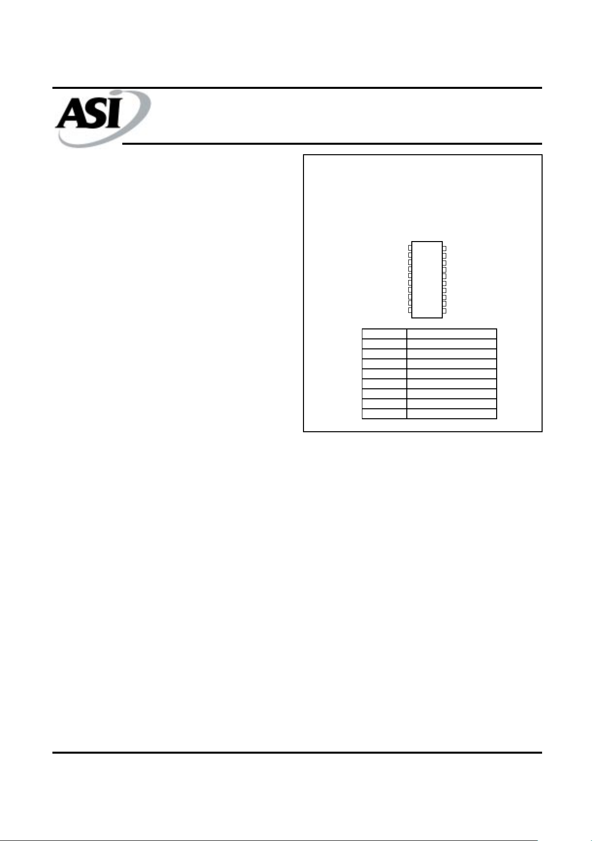
PIN ASSIGNMENT
(Top View)
A V AILABLE AS MILIT AR Y
SPECIFICA TIONS
• SMD 5962-90847
• MIL-STD-883
20-Pin DIP (JD)
20-Pin Flatpack (HR)
(400 MIL)
GENERAL DESCRIPTION
The SMJ44400 is a series of 4,194,304-bit dynamic random-access memories (DRAMs), organized as 1,048,576
words of four bits each. This series employs state-of-the-art
technology for high performance, reliability, and low-power
operation.
The SMJ44400 features maximum row access times of
80ns, 100ns, and 120ns. Maximum power dissipation is as
low as 360mW operating and 22mW standby.
All inputs and outputs, including clocks, are compatible
with Series 54 TTL. All addressses and data-in lines are latched
on-chip to simplify system design. Data out is unlatched to
allow greater system flexibility.
1M x 4 DRAM
D YNAMIC RANDOM-ACCESS
MEMORY
For more products and information
please visit our web site at
www.austinsemiconductor .com
• Single +5V ±10% power supply
• Enhanced Page-Mode operation for faster memory access
P Higher data bandwidth than conventional page-mode
parts
P Random Single-Bit Access within a row with a column
address
• CAS\-Before-RAS\ (CBR) Refresh
• Long Refresh period: 1024-cycle Refresh in 16ms (Max)
• 3-State unlatched Output
• Low Power Dissipation
• All Inputs/Outputs and Clocks are TTL Compatible
• Processing to MIL-STD-883, Class B available
1
2
3
4
5
6
7
8
9
10
20
19
18
17
16
15
14
13
12
11
DQ1
DQ2
W\
RAS\
A9
A0
A1
A2
A3
Vcc
Vss
DQ4
DQ3
CAS\
OE\
A8
A7
A6
A5
A4
The SMJ44400 is offered in a 400-mil, 20-pin ceramic
side-brazed dual-in-line package (JD suffix) and a 20-pin
ceramic flatpack (HR suffix) that are characterized for
operation from -55°C to +125°C.
OPERATION
Enhanced Page Mode
Enhanced page-mode operation allows faster memory
access by keeping the same row address while selecting
random column addresses. The time for row-address setup
and hold and address multiplex is eliminated. The maximum
number of columns that can be accessed is determined by the
maximum RAS\ low time and the CAS\ page cycle time used.
With minimum CAS\ page cycle time, all 1024 columns
specified by column addresses A0 through A9 can be accessed
without intervening RAS\ cycles.
Unlike conventional page-mode DRAMs, the columnaddress buffers in this device are activated on the
Pin Name Function
A0 - A9 Address Inputs
CAS\ Column-Address Strobe
DQ1 - DQ4 Data Inputs/Outputs
OE\ Output Enable
RAS\ Row-Address Strobe
W\ Write Enable
Vcc 5V Supply
Vss Ground

DRAM
SMJ44400
Austin Semiconductor, Inc.
SMJ44400
Rev. 2.0 10/01
Austin Semiconductor, Inc. reserves the right to change products or specifications without notice.
2
(continued)
Enhanced Paga Mode (continued)
falling edge of RAS\. The buffers act as transparent or flowthrough latches while CAS\ is high. The falling edge of CAS\
latches the column addresses. This feature allows the
SMJ44400 to operate at a higher data bandwidth then conventional page-mode parts, since data retrieval begins as soon as
column address is valid rather than when CAS\ goes low. This
performance improvement is referred to as enhanced page
mode. Valid column address can be presented immediately
after row address hold time has been satisfied, usually well in
advance of the maximum (access time from column address)
has been satisfied. In the event that column addresses for the
next cycle are valid at the time CAS\ goes high, access time
for the next cycle is determined by the later occurrence of
t
CAC
or t
CPA
(access time form rising edge of CAS\).
Address (A0-A9)
Twenty address bits are required to decode 1 of 1,048,576
storage cell locations. Ten row-address bits are set up on
inputs A0 through A9 and latched onto the chip by RAS\. The
ten column-address bits are set up on pins A0 through A9 and
latched onto the chip by CAS\. All addresses must be stable
on or before the falling edges of RAS\ and CAS\. RAS\ is
similar to a chip enable in that it activates the sense
amplifiers as well as the row decoder. CAS\ is used as a chip
select, activating the output buffer as well as latching the
address bits into the column-address buffer.
Write Enable (W\)
The read or write mode is selected through W\. A logic
high on the W\ input selects the read mode and a logic low
selects the write mode. The write-enable terminal can be
driven from standard TTL circuits without a pullup resistor.
The data input is disabled when the read mode is selected.
When W\ goes low prior to CAS\ (early write), data out
reamins in the high-impedance state for the entire cycle
permitting a write operation independent of the state of OE\.
This permits early-write operation to be completed with OE\
grounded.
Data In/Out (DQ1 - DQ4)
The high-impedance output buffer provides direct TTL
compatibility (no pullup resistor required) with a fanout of
two Series 54 TTL loads. Data out is the same polarity as data
in. The output is in the high-impedance (floating) state until
CAS\ and OE\ are brought low. In a read cycle the output
becomes valid after all access times are satisfied. The output
remains valid while CAS\ and OE\ are low. CAS\ or OE\ going
high returns it to the high-impedance state.
Output Enable (OE\)
OE\ controls the impedance of the output buffers. When
OE\ is high, the buffers remain in the high-impedance state.
Bringing OE\ low during a normal cycle activates the output
buffers, putting them in the low-impedance state. It is
necessary for both RAS\ and CAS\ to be brought low for the
output buffers to go into the low-impedance state. Once in
the low-ompedance state, they remain in the low-impedance
state until either OE\ or CAS\ is brought high.
Refresh
A refresh operation must be performed at least once every
16ms to retain data. This can be achieved by strobing each of
the 1024 rows (A0-A9). A normal read or write cycle
refreshes all bits in each row that is selected. A RAS\-only
operation can be used by holding CAS\ at the high (inactive)
level, conserving power as the output buffer remains in the
high-impedance state. Externally generated addresses must
be used for a RAS\-only refresh. Hidden refresh can be
performed while maintaining valid data at teh output pin. This
is accomplished by holding CAS\ at VIL after a read operation
and cycling RAS\ after a specified precharge period, similar
to a RAS\-only refresh cycle. The external address is ignored
during the hidden refresh cycles.
CAS\-before-RAS\ (CBR) and hidden refresh
CBR refresh is utilized by bringing CAS\ low earlier than
RAS\ (see parameter t
CSR
) and holding it low after RAS\ falls
(see parameter t
CSR
). For successive CBR refresh cycles,
CAS\ can remain low while cycling RAS\. The external
address is ignored and the refresh address is generated
internally. During CBR refresh cycles the outputs remain in
the high-impedance state.
Hidden refresh can be performed while maintaining valid
data at the output pins. Thsi is accomplished by holding CAS\
at VIL after a read operation. RAS\ is cycled after the
specified read cycle parameters are met. Hidden refresh can
also be used in conjuction with an early-write cycle. CAS\ is
maintained at VIL while RAS\ is cycled, once all the specified
early-write parameters are met. Externally generated
addresses must be used to specify the location to be accessed
during the initial RAS\ cycle of a hidden refresh operation.
Subsequent RAS\ cycles (refresh cycles) use the internallygenerated addresses and the external address is ignored.
Power Up
To achieve proper device operation, an initial pause of
200µs followed by a minimum of eight initialization cycles is
DRAM
SMJ44400
Austin Semiconductor, Inc.
SMJ44400
Rev. 2.0 10/01
Austin Semiconductor, Inc. reserves the right to change products or specifications without notice.
3
(continued)
Power Up (continued)
required after full Vcc level is achieved. These eight initialization cycles need to include at least one refresh (RAS\-only
or CBR) cycle.
Test Mode
An industry standard Design For Test (DFT) mode is
incorporated in the SMJ44400. A CBR with W\ low (WCBR)
cycle is used to enter test mode. In the test mode, data is
written into and read from eight sections of the array in
parallel. All data is written into the array through DQ1. Data
is comparted upon reading and if all bits are equal, all DQ pins
go high. If any one bit is different, all the DQ pins go low.
Any combination read, write, read-write, or page-mode can
be used in the test mode. The test mode function reduces test
times by enabling the 1M x 4-bit DRAM to be tested as if it
were a 512K DRAM where column address 0 is not used. A
RAS\-only or CBR refresh cycle is used to exit the DFT mode.
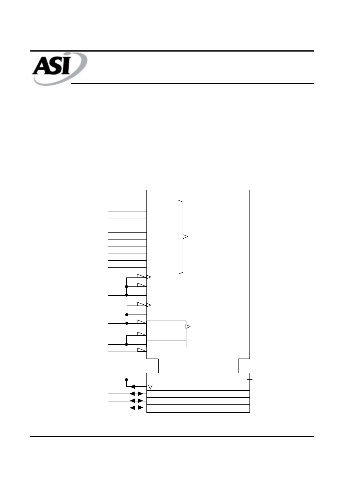
LOGIC SYMBOL
1
6
7
8
9
11
12
13
14
15
5
4
17
3
16
1
2
18
19
RAM 1024K x 4
A0
A1
A2
A3
A4
A5
A6
A7
A8
A9
RAS\
CAS\
W\
OE\
DQ1
DQ2
DQ3
DQ4
&
23,21D
G25
20D10/21D0
20D19/21D9
C20[Row]
G23/[Refresh Row]
24[Power Down]
C21[Column]
G24
23C22
24,25EN
A
0
1 048 575
A, 22D
26
A, Z26
1. This symbol is in accordance with ANSI/IEEE Std. 91-1984 and IEC Publication 617-12. The pinouts illustrated are for the JD package.
DRAM
SMJ44400
Austin Semiconductor, Inc.
SMJ44400
Rev. 2.0 10/01
Austin Semiconductor, Inc. reserves the right to change products or specifications without notice.
4
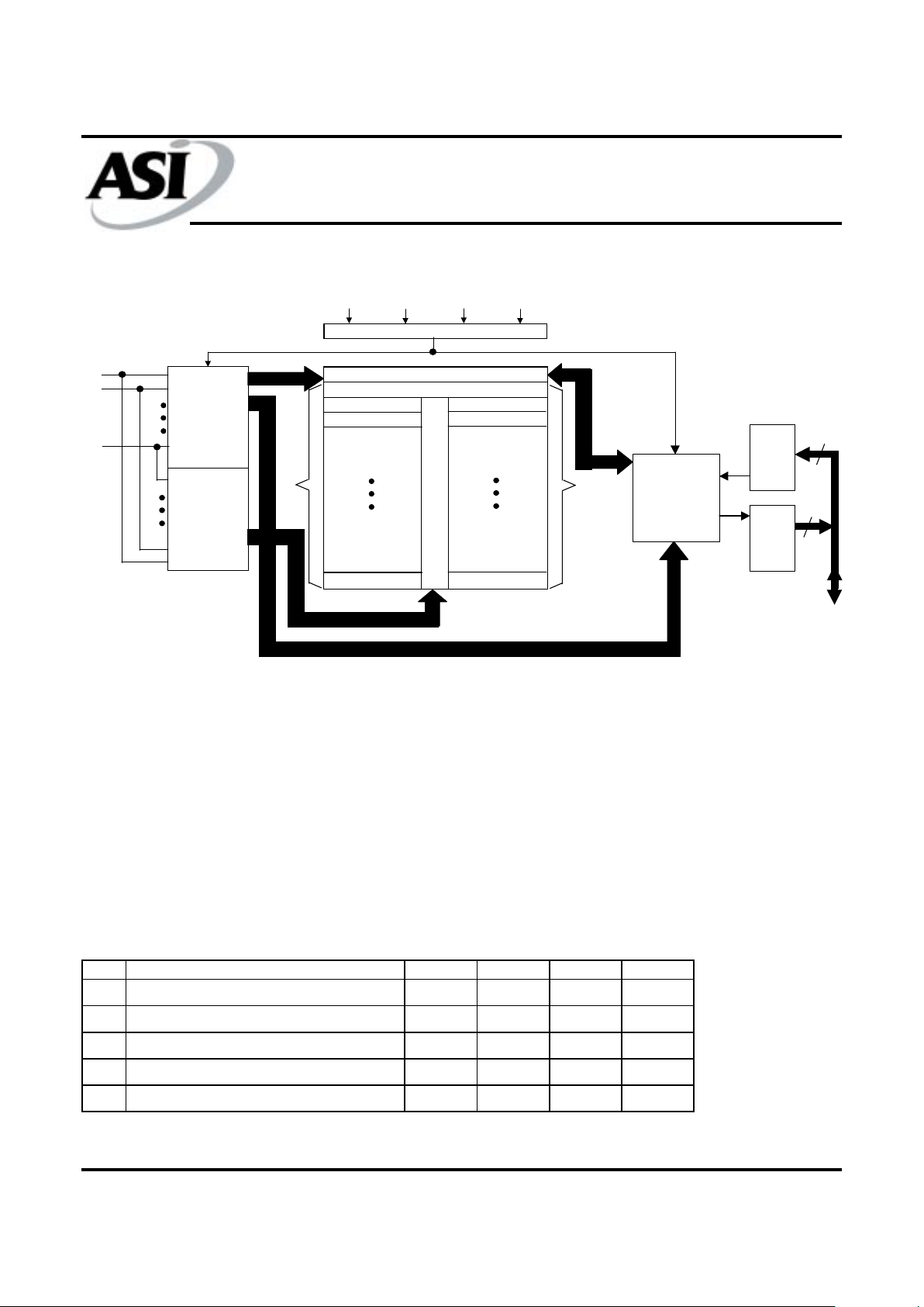
FUNCTIONAL BLOCK DIAGRAM
RAS\ CAS\ W\ OE\
A0
A1
A9
Timeing and Control
Column
Address
Buffers
Row
Address
Buffers
R
O
W
D
E
C
O
D
E
R
Column Decode
Sense Amplifiers
128K Array
128K Array
128K Array
128K Array
128K Array 128K Array
8
2
10
10
16 16
I/O
Buffers
4 of 16
Selection
Data
In
Reg.
Data
Out
Reg.
16
16
2
4
4
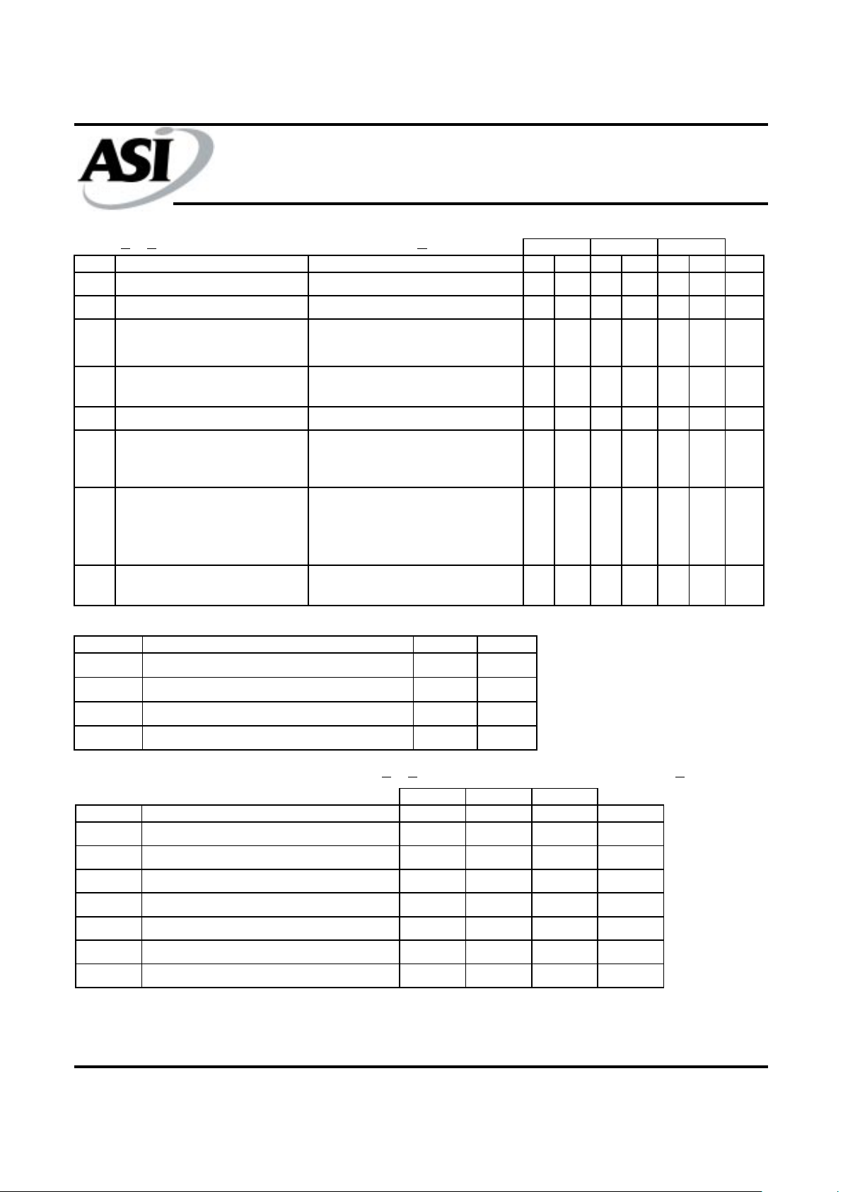
ABSOLUTE MAXIMUM RA TINGS*
Voltage on Vcc Supply Relative to Vss...............-1V to +7.0V
Voltage Range on Any Pin Relative to Vss.........-1V to +7.0V
Short Circuit Output Current (per I/O)….......................50mA
Power Dissipation.................................................................1W
Storage Temperature Range..........................-65°C to +150°C
Operating Temperature Range......................-55°C to +125°C
*Stresses greater than those listed under "Absolute
Maximum Ratings" may cause permanent damage to the
device. This is a stress rating only and functional operation of the device at these or any other conditions above
those indicated in the operation section of this specification is not implied. Exposure to absolute maximum rating
conditions for extended periods may affect reliability.
** Junction temperature depends upon package type,
cycle time, loading, ambient temperature and airflow.
RECOMMENDED OPERA TING CONDITIONS
SYM DESCRIPTION MIN NOM MAX UNIT
V
CC
Supply Voltage 4.5 5 5.5 V
V
IH
High-Level Input Voltage 2.4 6.5 V
V
IL
Low-Level Input Voltage
1
-1 0.8 V
T
A
Minimum Operating Temperature -55 °C
T
C
Maximum Operating Case Temperature 125 °C
1. The algebraic convention, where the more negative (less positive) limit is designated as minimum, is used for logic-voltage levels only.
DRAM
SMJ44400
Austin Semiconductor, Inc.
SMJ44400
Rev. 2.0 10/01
Austin Semiconductor, Inc. reserves the right to change products or specifications without notice.
5
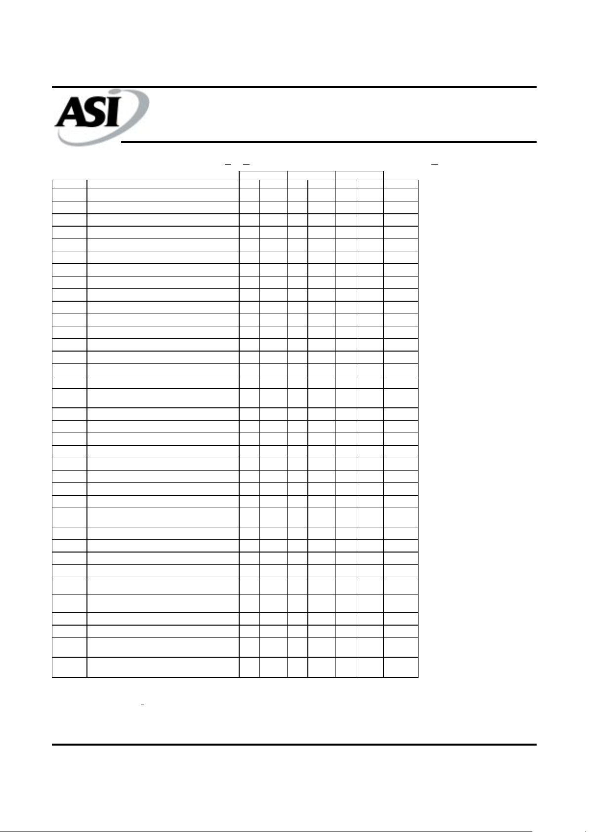
SYM PARAMETER TEST CONDITIONS MIN MAX MIN MAX MIN MAX UNIT
V
OH
High-level output voltage
I
OH
= -5mA
2.4 2.4 2.4 V
V
OL
Low-level output voltage
I
OL
= 4.2mA
0.4 0.4 0.4 V
I
I
Input current (leakage)
V
CC
= 5.5V, VI = 0V to 6.5V, All
other pins = 0V to V
CC
±10 ±10 ±10 µA
I
O
Output current (leakage)
V
CC
= 5.5V, VO = 0V to V
CC,
CAS\ High
±10 ±10 ±10 µA
I
CC1
Read - or write-cycle current
1
VCC = 5.5V, Minimum cycle
85 80 70 mA
I
CC2
Standby current
After 1 memory cycle,
RAS\ and CAS\ High,
V
IH
= 2.4V
444mA
I
CC3
Average refresh current
(RAS\ only, or CBR\)
1
VCC = 5.5V, Minimum cycle,
RAS\ cycling,
CAS\ High (RAS\ only),
RAS\ Low after CAS\ Low (CBR)
85 75 65 mA
I
CC4
Average page current
2
VCC = 5.5V, tPC = minimum,
RAS\ Low, CAS\ cycling
50 40 35 mA
-8 -10 -12
ELECTRICAL CHARACTERISTICS AND RECOMMENDED OPERA TING CONDITIONS
(-55oC<TA<125oC or -40oC to +85oC; Vcc = 5V +10%)
NOTES:
1. Measured with a maximum of one address change while RAS\ = VIL.
2. Measured with a maximum of one address change while CAS\ = VIH.
3. VCC = 5V ±0.5V and the bias on the pins under test is 0V. Capacitance is sampled only at initial design and after any major chang e.
4. t
OFF
and t
OEZ
are specified when the output is no longer driven. The outputs are disabled by bringing either OE\ or CAS\ High.
CAPACITANCE (f = 1MHz)
3
SYM PARAMETER MAX UNIT
C
i(A)
Input capacitance, address inputs 7 pF
C
i(RC)
Input capacitance, strobe inputs 10 pF
C
i(W)
Input capacitance, write-enable inputs 10 pF
C
O
Output capacitance 10 pF
SWITCHING CHARACTERISTICS (-55oC<TA<125oC or -40oC to +85oC; Vcc = 5V +10%)
-8 -10 -12
SYM PARAMETERS MAX MAX MAX UNIT
t
AA
Access time from column address 40 45 55 ns
t
CAC
Access time from CAS\ low 20 25 30 ns
t
CPA
Access time from column precharge 45 50 55 ns
t
RAC
Access time from RAS\ low 80 100 120 ns
t
OEA
Access time from OE\ low 20 25 30 ns
t
OFF
Output disable time after CAS\ High
4
20 25 30 ns
t
OEZ
Output disable tiem after OE\ High
4
20 25 30 ns
DRAM
SMJ44400
Austin Semiconductor, Inc.
SMJ44400
Rev. 2.0 10/01
Austin Semiconductor, Inc. reserves the right to change products or specifications without notice.
6
TIMING REQUIREMENTS (-55oC<TA<125oC or -40oC to +85oC; Vcc = 5V +10%)
SYM PARAMETER MIN MAX MIN MAX MIN MAX UNIT
t
RC
Cycle time, random read or write
1
150 180 210 ns
t
RWC
Cycle time, read-write 205 245 285 ns
t
PC
Cycle time, page-mode read or write
2
50 60 65 ns
t
PRWC
Cycle time, page-mode read-write 100 120 135 ns
t
RASP
Pulse duration, page mode, RAS\ low
3
80 100000 100 100000 120 100000 ns
t
RAS
Pulse duration, nonpage mode, RAS\ low
3
80 10000 100 10000 120 10000 ns
t
CAS
Pulse duration, CAS\ low
4
20 10000 25 10000 30 10000 ns
t
CP
Pulse duration, CAS\ High 10 10 15 ns
t
RP
Pulse duration, RAS\ High (precharge) 60 70 80 ns
t
WP
Pulse duration, write 15 20 25 ns
t
ASC
Setup time, column address before CAS\ low 0 0 0 ns
t
ASR
Setup time, row address before RAS\ low 0 0 0 ns
t
DS
Setup time, data
5
000 ns
t
RCS
Setup time, read before CAS\ low 0 0 0 ns
t
CWL
Setup time, W\ low before CAS\ high 20 25 30 ns
t
RWL
Setup time, W\ low before RAS\ high 20 25 30 ns
t
WCS
Setup time, W\ low before CAS\ low
(early-write operation only)
000 ns
t
WSR
Setup time, W\ High (CBR refresh only) 10 10 10 ns
t
CAH
Hold time, column address after CAS\ low 15 20 20 ns
t
DHR
Hold time, data after RAS\ low 60 75 90 ns
t
DH
Hold time, data
5
15 20 25 ns
t
AR
Hold time, column address after CAS\ low
4
60 75 90 ns
t
RAH
Hold time, row address after RAS\ low 10 15 15 ns
t
RCH
Hold time, read after CAS\ High
6
000 ns
t
RRH
Hold time, read after RAS\ High
6
000 ns
t
WCH
Hold time, write after CAS\ low
(early-write operation only)
15 20 25 ns
t
WCR
Hold time, write after RAS\ low
4
60 75 90 ns
t
WHR
Hold time, W\ High (CBR refresh only) 10 10 10 ns
t
OEH
Hold time, OE\ command 20 25 30 ns
t
ROH
Hold time, RAS\ referenced to OE\ 20 25 30 ns
t
AWD
Delay time, column address to W\ low
(read-write operation only)
70 80 90 ns
t
CHR
Delay time, RAS\ low to CAS\ High
(CBR refresh only)
20 20 25 ns
t
CRP
Delay time, CAS\ High to RAS\ low 0 0 0 ns
t
CSH
Delay time, RAS\ low to CAS\ High 80 100 120 ns
t
CSR
Delay time, CAS\ low to RAS\ low
(CBR refresh only)
10 10 10 ns
t
CWD
Delay time, CAS\ low to W\ low
(read-write operation only)
50 60 70 ns
-8 -10 -12
NOTES:
1. All cycle times assume tT = 5ns.
2. To assure tPC min, t
ASC
should be > tCP.
3. In a read-write cycle, t
RWD
and t
RWL
must be observed.
4. In a read-write cycle, t
CWD
and t
CWL
must be observed.
5. Referenced to the later of CAS\ or W\ in write operations.
6. Either t
RRH
or t
RCH
must be satisfied for a read cycle.
DRAM
SMJ44400
Austin Semiconductor, Inc.
SMJ44400
Rev. 2.0 10/01
Austin Semiconductor, Inc. reserves the right to change products or specifications without notice.
7
TIMING REQUIREMENTS (continued)
SYM PARAMETER MIN MAX MIN MAX MIN MAX UNIT
t
RAD
Delay time, RAS\ low to column address
1
15 40 20 50 20 65 ns
t
RAL
Delay time, column addresss to RAS\ High 40 50 55 ns
t
CAL
Delay time, column addresss to CAS\ High 40 50 55 ns
t
RCD
Delay time, RAS\ low to CAS\ low
1
20 60 25 75 25 90 ns
t
RPC
Delay time, RAS\ High to CAS\ low 0 0 0 ns
t
RSH
Delay time, CAS\ low to RAS\ High 20 25 30 ns
t
RWD
Delay time, RAS\ low to W\ low
(read-write operation only)
110 135 160 ns
t
CLZ
CAS\ to output in low Z
2
000 ns
t
OED
OE\ to data delay 20 25 30 ns
t
REF
Refresh time interval 16 16 16 ms
t
T
Tranistion time
3
-8 -10 -12
NOTES:
1. Maximum value specified only to assure access time.
2. Valid data is presented at the outputs after all access times are satisfied but can go from the high-impedance state to an invalid-data state prior to the specified access times as the outputs are driven when
CAS\ and OE\ are low.
3. Transition times (rise and fall) for RAS\ and CAS\ are to be a minimum of 3ns and a maximum of 50ns.
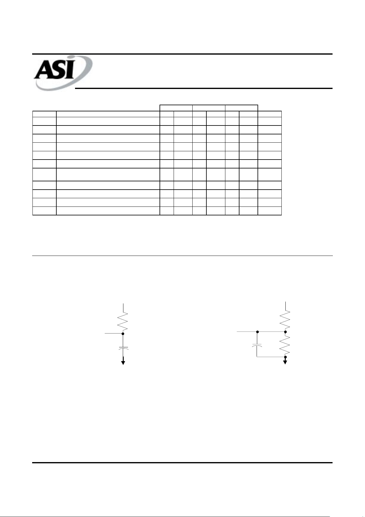
P ARAMETER MEASUREMENT INFORMA TION
Figure 1. Load Circuit for Timing Parameters
1.31V
Output Under Test
RL = 218Ω
CL = 100 pF
1
5V
Output Under Test
R1 = 828Ω
R2 = 295Ω
CL = 100 pF
1
(b) AL TERNA TE LOAD CIRCUIT
(a) LOAD CIRCUIT
NOTES:
1. CL includes probe and fixture capacitance.
 Loading...