

AUSTIN SMJ27C010A-12JM, SMJ27C010A-15JM, SMJ27C010A-20JM Datasheet
Austin Semiconductor, Inc.
UVEPROM
SMJ27C010A
1 MEG UVEPROM
UV Erasable Programmable
Read-Only Memory
A VAILABLE AS MILITA R Y
SPECIFICATIONS
• SMD 5962-89614
• MIL-STD-883
FEATURES
• Organized 131,072 x 8
• Single +5V ±10% power supply
• Operationally compatible with existing megabit EPROMs
• Industry standard 32-pin ceramic dual-in-line package
• All inputs/outputs fully TTL compatible
• 8-bit output for use in microprocessor-based systems
• Very high-speed SNAP! Pulse Programming
• Power-saving CMOS technology
• 3-state output buffers
• 400mV minimum DC noise immunity with standard
TTL loads
• Latchup immunity of 250 mA on all input and output pins
• No pullup resistors required
• Low power dissipation (Vcc = 5.5V)
PActive - 165 mW Worst Case
PStandby - 0.55 mW Worst Case (CMOS-input levels)
OPTIONS MARKING
• Timing
120ns access -1 2
150ns access -1 5
200ns access -2 0
• Package(s)
Ceramic DIP (600mils) J No. 114
• Operating Temperature Ranges
Military (-55oC to +125oC) M
For more products and information
please visit our web site at
www.austinsemiconductor.com
SMJ27C010A
Rev. 1.0 9/01
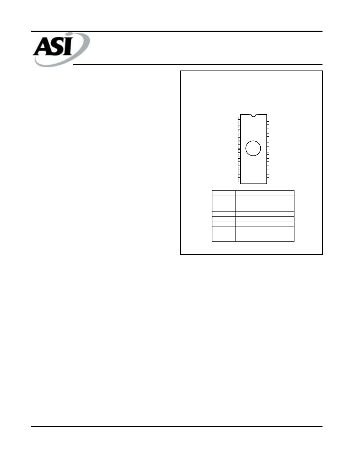
PIN ASSIGNMENT
(Top View)
32-Pin DIP (J)
(600 MIL)
1
V
PP
2
A16
3
A15
4
A12
5
A7
6
A6
7
A5
8
A4
9
A3
10
A2
11
A1
12
A0
13
DQ0
14
DQ1
15
DQ2
16
GND
Pin Name Function
A0 - A18 Address Inputs
DA0-DQ7 Inputs (programming)/Outputs
E\ Chip Enable
G\ Output Enable
GND Ground
PGM\ Program
V
5V Supply
CC
V
13V Power Supply*
PP
*Only in program mode.
Vcc
32
PGM\
31
NC
30
A14
29
A13
28
A8
27
A9
26
A11
25
G\
24
A10
23
22
E\
21
DQ7
20
DQ6
19
DQ5
18
DQ4
17
DQ3
GENERAL DESCRIPTION
The SMJ27C010A series are 131072 by 8-bit (1048576bit), ultaviolet (UV) light erasable, electrically programmable
read-only memories (EPROMs).
These devices are fabricated using power-saving CMOS
technology for high speed and simple interface with MOS and
bipolar circuits. All inputs (including program data inputs)
can be driven by Series 54 TTL circuits without the use of
external pullup resistors. Each output can drive one Series 54
TTL circuit without external resistors.
The SMJ27C010A EPROM is offered in a ceramic
dual-in-line package (J suffix) designed for insertion in
mounting-hole rows on 15.2mm (600mil) centers.
These EPROMs operate from a single 5V supply (in the
read mode), and therefore, are ideal for use in
microprocessor-based systems. One other 13V supply is
needed for programming. All programming signals are TTL
level. These devices are programmable using the SNAP! Pulse
programming algorithm. The SNAP! Pulse programming
algorithm uses a VPP of 13V and a VCC of 6.5V for a nominal
programming time of thirteen seconds. For programming
outside the system, existing EPROM programmers can be
used. Locations can be programmed singly, in blocks, or at
random.
Austin Semiconductor, Inc. reserves the right to change products or specifications without notice.
1
Austin Semiconductor, Inc.
FUNCTIONAL BLOCK DIAGRAM*
EPROM 131,072 x 8
12
A0
11
A1
10
A2
9
A3
8
A4
7
A5 DQ0
6
A6 DQ1
5
A7 DQ2
27
A8 DQ3
26
A9 DQ4
E\
G\
23
25
4
28
29
3
2
22
24
A10 DQ5
A11 DQ6
A12 DQ7
A13
A14
A15
A16
0
A
16
[PWR DWN]
&
EN
0
131,071
A
A
A
A
A
A
A
A
UVEPROM
SMJ27C010A
13
14
15
17
18
19
20
21
* This symbol is in accordance with ANSI/IEEE Std 91-1984 and IEC Publication 617-12. J package illustrated.
OPERATION
The seven modes of operation are listed in Table 1. The read mode requires a single 5V supply. All inputs are TTL level
except for VPP during programming (13V for SNAP! Pulse), and 12V on A9 for signature mode.
TABLE 1. OPERATION MODES
MODE*
FUNCTION
E\
G\
READ
V
V
PGM\ X X X
V
PP
V
CC
V
V
A9 X X X X X X
A0 X X X X X X
DQ0-DQ7 Data Out High-Z High-Z Data In Data Out High-Z
* X can be VIL or VIH.
= 12V ± 0.5V
**V
H
SMJ27C010A
Rev. 1.0 9/01
IL
IL
CC
CC
OUTPUT
DISABLE
V
IL
V
IH
V
CC
V
CC
STANDBY PROGRAMMING VERIFY
V
IH
X
V
CC
V
CC
V
IL
V
IH
V
IL
V
PP
V
CC
V
IL
V
IL
V
IH
V
PP
V
CC
Austin Semiconductor, Inc. reserves the right to change products or specifications without notice.
2
PROGRAM
INHIBIT
V
IH
X
X
V
PP
V
CC
SIGNATURE MODE
V
IL
V
IL
X
V
CC
V
CC
** VH**
V
H
V
IL
V
IH
CODE
MFG DEVICE
97 D6

Austin Semiconductor, Inc.
UVEPROM
SMJ27C010A
READ/OUTPUT DISABLE
When the outputs of two or more SMJ27C010As are
connected in parallel on the same bus, the output of any
particular device in the circuit can be read with no
interference from competing outputs of the other devices. To
read the output of a single device, a low level signal is applied
to the E\ and G\ pins. All other devices in the circuit should
have their outputs disabled by applying a high-level signal to
one of these pins.
LA TCHUP IMMUNITY
Latchup immunity on the SMJ27C010A is a minimum of
250mA on all inputs and outputs. This feature provides latchup
immunity beyond any potential transients at the printed
circuit board level when the devices are interfaced to
industry-standard TTL or MOS logic devices. The input/
output layout approach controls latchup without
compromising performance or packing density.
POWER DOWN
Active ICC supply current can be reduced from 30mA to 500µA
by applying a high TTL input on E\ and to 100µA by applying a
high CMOS input on E\. In this mode all outputs are in the
high-impedance state.
ERASURE
Before programming, the SMJ27C010A EPROM is erased
by exposing the chip through the transparent lid to a highintensity ultraviolet light (wavelength 2537 Å). The
recommended minimum exposure dose (UV intensity x
exposure time) is 15-W.s/cm2. A typical 12-mW/cm2,
filterless UV lamp erases the device in 21 minutes. The lamp
should be located about 2.5cm above the chip during erasure.
After erasure, all bits are in the high state. It should be noted
that normal ambient light contains the correct wavelength for
erasure; therefore, when using the SMJ27C010A, the window
should be covered with an opaque label. After erasure (all
bits in logic high state), logic lows are programmed into the
desired locations. A programmed low can be erased only by
ultraviolet light.
SNAP! PULSE PROGRAMMING
The SMJ27C010A is programmed by using the SNAP! Pulse
programming algorithm as illustrated by the flow chart
(Figure 1). This algorithm programs in a nominal time of
thirteen seconds. Actual programming time varies as a
function of the programmer used.
The SNAP! Pulse programming algorithm uses an initial pulse
of 100 microseconds (µs) followed by a byte verification to
determine when the addressed byte has been successfully
programmed. Up to ten 100µs pulses per byte are provided
before a failure is recognized.
The programming mode is achieved when V
VCC= 6.5V, E\ = VIL, and G\ = VIH. Data is presented in
parallel (eight bits) on pins DQ0 through DQ7. Once addresses
and data are stable, PGM\ is pulsed low.
More than one device can be programmed when the devices
are connected in parallel. Locations can be programmed in
any order. When the SNAP! Pulse programming routine is
complete, all bits are verified with VCC = VPP = 5V ± 10%.
= 13V,
PP
PROGRAM INHIBIT
Programming can be inhibited by maintaining high level
inputs on the E\ or the PGM\ pins.
PROGRAM VERIFY
Programmed bits can be verified with VPP = 13V when
G\ = VIL, and E\ = VIL, and PGM\ = VIH.
SIGNA TURE MODE
The signature mode provides access to a binary code
identifying the manufacturer and type. This mode is activated
when A9 (pin 26) is forced to 12V. Two identifier bytes are
accessed by toggling A0. All other addresses must be held
low. The signature code for these devices is 97D6. A0 low
selects the manufacturer’s code 97 (Hex), and A0 high
selects the device code D6 (Hex), as shown in Table 2.
TABLE 2. SIGNATURE MODES
IDENTIFIER*
MANUFACTURER CODE
DEVICE CODE
* E\ = G\ = VIL, A1 - A8 = VIL, A9 = VH, A10 - A16 = VIL, VPP = VCC.
SMJ27C010A
Rev. 1.0 9/01
A0 DQ7 DQ6 DQ5 DQ4 DQ3 DQ2 DQ1 DQ0 HEX
V
IL
V
IH
1001011197
11010110D6
3
PINS
Austin Semiconductor, Inc. reserves the right to change products or specifications without notice.

UVEPROM
SMJ27C010A
Austin Semiconductor, Inc.
FIGURE 1. SNAP! PULSE PROGRAMMING FLOW CHART
START
Address = First Location
Increment
Address
VCC = 6.5V ± 0.25V, VPP = 13V ± 0.25V
Program One Pulse = tW = 100µs
Last
Address?
Yes
Address = First Location
X = 0
Verify
One
Byte
Pass
Fail
Increment Address
Program One Pulse = tW = 100µs
No
X = X+1
X = 10?
Program
Mode
Interactive
Mode
SMJ27C010A
Rev. 1.0 9/01
No
VCC = VPP = 5V ± 0.5V
Last
Address?
Yes
Compare
All Bytes
to Original
Data
Pass
Device Passed
Fail
Yes
Device Failed
Final
Verification
Austin Semiconductor, Inc. reserves the right to change products or specifications without notice.
4
 Loading...