


AUSTIN MT4C4001JECJ-8-IT, MT4C4001JECJ-8-883C, MT4C4001JECJ-12-IT, MT4C4001JECJ-12-XT, MT4C4001JECJ-7-883C Datasheet
...
DRAM
MT4C4001J
Austin Semiconductor, Inc.
MT4C4001J
Rev. 1.0 9/01
Austin Semiconductor, Inc. reserves the right to change products or specifications without notice.
1
For more products and information
please visit our web site at
www.austinsemiconductor.com
AVAILABLE AS MILITARY
SPECIFICATIONS
• SMD 5962-90847
• MIL-STD-883
1 MEG x 4 DRAM
Fast Page Mode DRAM
FEATURES
• Industry standard x4 pinout, timing, functions, and
packages
• High-performance, CMOS silicon-gate process
• Single +5V±10% power supply
• Low-power, 2.5mW standby; 300mW active, typical
• All inputs, outputs, and clocks are fully TTL and CMOS
compatible
• 1,024-cycle refresh distributed across 16ms
• Refresh modes: RAS\-ONLY, CAS\-BEFORE-RAS\
(CBR), and HIDDEN
• FAST PAGE MODE access cycle
• CBR with WE\ a HIGH (JEDEC test mode capable via
WCBR)
OPTIONS MARKING
• Timing
70ns access -7
80ns access -8
100ns access -1 0
120ns access -1 2
• Packages
Ceramic DIP (300 mil) CN No. 103
Ceramic DIP (400 mil) C No. 104
Ceramic LCC* ECN No. 202
Ceramic ZIP CZ No. 400
Ceramic SOJ EC J No. 504
Ceramic Gull Wing ECG No. 600
*NOTE: If solder-dip and lead-attach is desired on LCC
packages, lead-attach must be done prior to the solderdip operation.
PIN ASSIGNMENT
(Top View)
20-Pin DIP (C, CN)
1
2
3
4
5
6
7
8
9
10
20
19
18
17
16
15
14
13
12
11
DQ1
DQ2
WE\
RAS\
A9
A0
A1
A2
A3
Vcc
Vss
DQ4
DQ3
CAS\
OE\
A8
A7
A6
A5
A4
1
2
3
4
5
9
10
11
12
13
26
25
24
23
22
18
17
16
15
14
DQ1
DQ2
WE\
RAS\
A9
A0
A1
A2
A3
Vcc
Vss
DQ4
DQ3
CAS\
OE\
A8
A7
A6
A5
A4
20-Pin SOJ (ECJ),
20-Pin LCC (ECN), &
20-Pin Gull Wing (ECG)
GENERAL DESCRIPTION
The MT4C4001J is a randomly accessed solid-state
memory containing 4,194,304 bits organized in a x4
configuration. During READ or WRITE cycles each bit is
uniquely addressed through the 20 address bits which are
entered 10 bits (A0-A9) at a time. RAS\ is used to latch the
first 10 bits and CAS\ the later 10 bits. A READ or WRITE
cycle is selected with the WE\ input. A logic HIGH on WE\
dictates READ mode while a logic LOW on WE\ dictates
WRITE mode. During a WRITE cycle, data-in (D) is latched
by the falling edge of WE\ or CAS\, whichever occurs last. If
WE\ goes LOW prior to CAS\ going LOW, the output pin(s)
remain open (High-Z) until the next CAS\ cycle. If WE\ goes
LOW after data reaches the output pin(s), Qs are activated and
retain the selected cell data as long as CAS\ remains low
(regardless of WE\ or RAS\). This LATE WE\ pulse results in
a READ-WRITE cycle. The four data inputs and four data
outputs are routed through four pins using common I/O and
pin direction is controlled by WE\ and OE\. FAST-PAGEMODE operations allow faster data operations (READ,
WRITE, or READ-MODIFY-WRITE) within a row address
(A0-A9) defined page boundary . The FAST PAGE MODE
(continued)
20-Pin DIP (CZ)
OE\ 1
DQ3 3
Vss 5
DQ2 7
RAS\ 9
A0 11
A2 13
Vcc 15
A5 17
A7 19
2 CAS\
4 DQ4
6 DQ1
8 WE\
10 A9
12 A1
14 A3
16 A4
18 A6
20 A8
DRAM
MT4C4001J
Austin Semiconductor, Inc.
MT4C4001J
Rev. 1.0 9/01
Austin Semiconductor, Inc. reserves the right to change products or specifications without notice.
2
GENERAL DESCRIPTION (cont.)
cycle is always initiated with a row address strobe-in by RAS\
followed by a column address strobed-in by CAS\. CAS\ may
be toggled-in by holding RAS\ LOW and strobing-in different
column addresses, thus executing faster memory cycles.
Returning RAS\ HIGH terminates the FAST PAGE MODE
operation.
Returning RAS\ and CAS\ HIGH terminates a memory cycle
and decreases chip current to a reduced standby level. Also,
the chip is preconditioned for the next cycle during the RAS\
HIGH time. Memory cell data is retained in its corrected
stated by maintaining power and executing any RAS\ cycle
(READ, WRITE, RAS\-ONLY, CAS\-BEFORE-RAS\, or
HIDDEN REFRESH) so that all 1,024 combinations of RAS\
addresses (A0-A9) are executed at least every 16ms,
regardless of sequence. The CBR REFRESH cycle will
invoke the internal refresh counter for automatic RAS\
addressing.
FUNCTIONAL BLOCK DIAGRAM
FAST PAGE MODE
WE\ DQ1
CAS\ DQ2
DQ3
DQ4
OE\
Vcc
A0 Vss
A1
A2
A3
A4
A5
A6
A7
A8
A9
RAS\
NO. 2 CLOCK
GENERATOR
NO. 1 CLOCK
GENERATOR
COLUMN
ADDRESS
BUFFER
REFRESH
CONTROLLER
REFRESH
COUNTER
ROW ADDRESS
BUFFERS (10)
*EARLY-WRITE
DETECTION CIRCUIT
DATA IN
BUFFER
DATA OUT
BUFFER
COLUMN
DECODER
SENSE AMPLIFIERS
I/O GATING
MEMORY
ARRAY
ROW
DECODER
1024
1024 x 4
4
4
4
4
10
10
10
10
10
NOTE: WE\ LOW prior to CAS\ LOW, EW detection circuit output is a HIGH (EARLY-WRITE)
CAS\ LOW prior to WE\ LOW, EW detection circuit output is a LOW (LATE-WRITE)
DRAM
MT4C4001J
Austin Semiconductor, Inc.
MT4C4001J
Rev. 1.0 9/01
Austin Semiconductor, Inc. reserves the right to change products or specifications without notice.
3
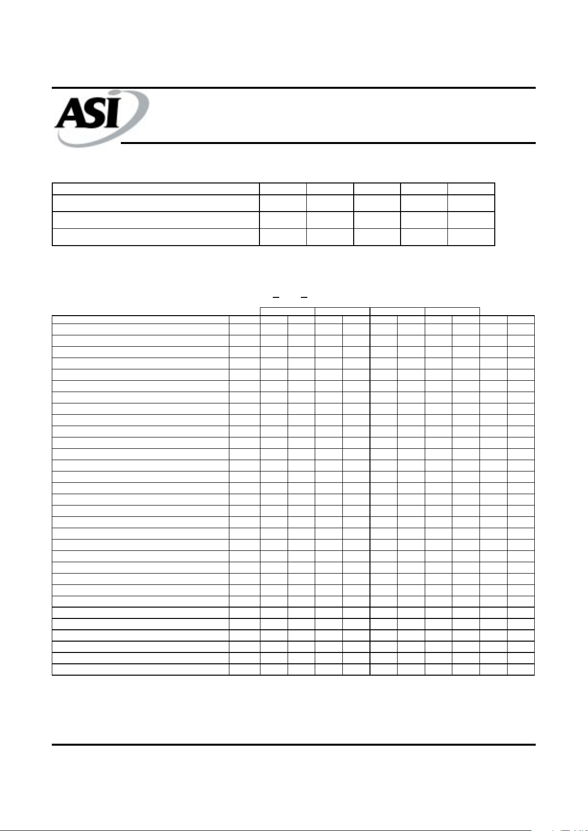
TRUTH TABLE
DATA IN/OUT
t
R
t
C
DQ1-DQ4
HH
XXXXX High-Z
L L H L ROW COL Data Out
L L L X ROW COL Data In
LLH
LLH ROW COL Data Out/Data In
1st Cycle L HL H L ROW COL Data Out
2nd Cycle L HL H L n/a COL Data Out
1st Cycle L HL L X ROW COL Data In
2nd Cycle L HL L X n/a COL Data In
1st Cycle L HLHLLH ROW COL Data Out/Data In
2nd Cycle L HLHLLH n/a COL Data Out/Data In
L H X X ROW n/a High-Z
READ LHL L H L ROW COL Data Out
WRITE LHL L L X ROW COL Data In
HL L H X X X High-Z
HIDDEN REFRESH
CAS\-BEFORE-RAS\ REFRESH
FAST-PAGE-MODE
READ-WRITE
FAST-PAGE-MODE
READ
FAST-PAGE-MODE
EARLY-WRITE
RAS\-ONLY REFRESH
Standby
READ
EARLY-WRITE
READ-WRITE
ADDRESSES
FUNCTION RAS\ CAS\ WE\ OE\
DRAM
MT4C4001J
Austin Semiconductor, Inc.
MT4C4001J
Rev. 1.0 9/01
Austin Semiconductor, Inc. reserves the right to change products or specifications without notice.
4
ABSOLUTE MAXIMUM RATINGS*
Voltage on Any Pin Relative to Vss.................-1.0V to +7.0V
Storage Temperature.......................................-65oC to +150oC
Power Dissipation.................................................................1W
Short Circuit Output Current...........................................50mA
Lead Temperature (soldering 5 seconds).....................+270oC
*Stresses greater than those listed under "Absolute Maximum
Ratings" may cause permanent damage to the device. This is
a stress rating only and functional operation of the device at
these or any other conditions above those indicated in the
operation section of this specification is not implied.
Exposure to absolute maximum rating conditions for extended
periods may affect reliability.
ELECTRICAL CHARACTERISTICS AND RECOMMENDED DC OPERATING CONDITIONS
(NOTES: 1, 3, 4, 6, 7) (-55°C < TA < 125°C; VCC = 5V ±10%)
PARAMETER/CONDITION SYM MIN MAX UNITS NOTES
Supply Voltage
V
CC
4.5 5.5 V
Input High (Logic 1) Voltage, All Inputs
V
IH
2.4
V
CC
+0.5
V
Input Low (Logic 0) Voltage, All Inputs
V
IL
-0.5 0.8 V
INPUT LEAKAGE CURRENT
Any Input 0V <
V
IN
< 5.5V Vcc = 5.5V
(All other pints not under test = 0V)
I
I
-5 5 µA
OUTPUT LEAKAGE CURRENT
(Q is Disabled, 0V <
V
OUT
< 5.5V) Vcc = 5.5V
I
OZ
-5 5 µA
V
OH
2.4 V
V
OL
0.4 V
OUTPUT LEVELS
Output High Voltage (I
OUT
= -5mA)
Output Low Voltage (I
OUT
= 4.2mA)
PARAMETER/CONDITION SYM -7 -8 -10 -12 UNITS NOTES
STANDBY CURRENT (TTL)
(RAS\ = CAS\ = V
IH
)
I
CC1
4444mA
STANDBY CURRENT (CMOS)
(RAS\ = CAS\ = V
CC
-0.2V; all other inputs = VCC -0.2V)
I
CC2
2222mA
OPERATING CURRENT: Random READ/WRITE
Average Power-Supply Current
(RAS\, CAS\, Address Cycling: t
RC
= tRC(MIN))
I
CC3
85 75 65 70 mA 3, 4
OPERATING CURRENT: FAST PAGE MODE
Average Power-Supply Current
(RAS\ = V
IL
, CAS\, Address Cycling: tPC = tPC (MIN))
I
CC4
60 50 45 40 mA 3, 4
REFRESH CURRENT: RAS\-ONLY
Average Power-Supply Current
(RAS\ Cycling, CAS\ = V
IH
: tRC = tRC (MIN))
I
CC5
85 75 65 70 mA 3
REFRESH CURRENT: CAS\-BEFORE-RAS\
Average Power-Supply Current
(RAS\, CAS\, Address Cycling: t
RC
= tRC (MIN))
I
CC6
85 75 65 70 mA 3, 5
MAX
DRAM
MT4C4001J
Austin Semiconductor, Inc.
MT4C4001J
Rev. 1.0 9/01
Austin Semiconductor, Inc. reserves the right to change products or specifications without notice.
5
CAPACITANCE
ELECTRICAL CHARACTERISTICS AND RECOMMENDED AC OPERATING CONDITIONS
(NOTES: 6, 7, 8, 9, 10, 11, 12, 13) (-55°C < TC < 125°C; VCC = 5V ±10%)
PARAMETER SYM MIN MAX UNITS NOTES
Input Capacitance: A0-A10
C
I1
7pF2
Input Capacitance: RAS\, CAS\, WE\, OE\
C
I2
7pF2
Input/Output Capacitance: DQ
C
IO
8pF2
PARAMETER SYM MIN MA X MIN MAX MIN MAX MIN MAX UNITS NOTES
Random READ or WRITE cycle time
t
RC
130 150 190 220 ns
READ-WRITE cycle time
t
RWC
180 200 240 255 ns
FAST-PAGE-MODE READ or WRITE cycle time
t
PC
40 45 55 70 ns
FAST-PAGE-MODE READ-WRITE cycle time
t
PRWC
90 90 110 140 ns
Access time from RAS\
t
RAC
70 80 90 120 ns 14
Access time from CAS\
t
CAC
20 20 25 30 ns 15
Access time from column address
t
AA
35 40 45 60 ns
Access time from CAS\ precharge
t
CPA
35 40 45 60 ns
RAS\ pulse width
t
RAS
70 10,000 80 10,000 100 10,000 120 100,000 ns
RAS\ pulse width (FAST PAGE MODE)
t
RASP
70 100,000 80 100,000 100 100,000 120 100,000 ns
RAS\ hold time
t
RSH
20 20 25 30 ns
RAS\ precharge time
t
RP
50 60 70 90 ns
CAS\ pulse width
t
CAS
20 10,000 20 10,000 25 10,000 30 ns
CAS\ hold time
t
CSH
70 80 100 120 ns
CAS\ precharge time
t
CPN
10 10 12 15 ns 16
CAS\ precharge time (FAST PAGE MODE)
t
CP
10 10 12 15 ns
RAS\ to CAS\ delay time
t
RCD
20 50 20 60 25 75 25 90 ns 17
CAS\ to RAS\ precharge time
t
CRP
5 5 5 10 ns
Row address setup time
t
ASR
0000ns
Row address hold time
t
RAH
10 10 15 15 ns
RAS\ to column address delay time
t
RAD
15 35 15 40 20 50 20 60 ns 18
Column address setup time
t
ASC
0000ns
Column address hold time
t
CAH
15 15 20 25 ns
Column address hold time (referenced to RAS\)
t
AR
50 60 70 85 ns
Column address to RAS\ lead time
t
RAL
35 40 50 60 ns
Read command setup time
t
RCS
0000ns
Read command hold time (referenced to CAS\)
t
RCH
0000ns19
Read command hold time (referenced to RAS\)
t
RRH
0000ns19
CAS\ to output in Low-Z
t
CLZ
0000ns
Output buffer turn-off delay
t
OFF
0 20 0 20 0 20 0 20 ns 20
WE\ command setup time
t
WCS
0000ns21, 27
-7 -8 -10 -12
DRAM
MT4C4001J
Austin Semiconductor, Inc.
MT4C4001J
Rev. 1.0 9/01
Austin Semiconductor, Inc. reserves the right to change products or specifications without notice.
6
ELECTRICAL CHARACTERISTICS AND RECOMMENDED AC OPERATING CONDITIONS
(NOTES: 6, 7, 8, 9, 10, 11, 12, 13) (-55°C < TC < 125°C; VCC = 5V ±10%)
PARAMETER SYM MIN MAX MIN MAX MIN MAX MIN MAX UNITS NOTES
Write command hold time
t
WCH
15 15 20 25 ns
Write command hold time (referenced to RAS\)
t
WCR
50 60 70 80 ns
Write command pulse width
t
WP
15 15 20 25 ns
Write command to RAS\ lead time
t
RWL
20 20 25 30 ns
Write commend to CAS\ lead time
t
CWL
20 20 25 30 ns
Data-in setup time
t
DS
0000ns22
Data-in hold time
t
DH
12 15 18 25 ns 22
Data-in hold time (referenced to RAS\)
t
DHR
50 60 70 90 ns
RAS\ to WE\ delay time
t
RWD
95 105 130 140 ns 21
Column address to WE\ delay time
t
AWD
60 65 80 90 ns 21
CAS\ to WE\ delay time
t
CWD
45 45 55 60 ns 21
Transition time (rise or fall)
t
T
3 50 3 50 3 50 3 50 ns
Refresh period (1,024 cycles)
t
REF
16 16 16 16 ns
RAS\ to CAS\ precharge time
t
RPC
0000ns
CAS\ setup time (CAS\-BEFORE-RAS\ REFRESH)
t
CSR
5 101010ns5
CAS\ hold time (CAS\-BEFORE-RAS\ REFRESH)
t
CHR
10 15 20 25 ns 5
WE\ hold time (CAS\-BEFORE-RAS\ REFRESH)
t
WRH
10 10 10 10 ns 25, 28
WE\ setup time (CAS\-BEFORE-RAS\ REFRESH)
t
WRP
10 10 10 10 ns 25, 28
WE\ hold time (WCBR test cycle)
t
WTH
10 10 10 10 ns 25, 28
WE\ setup time (WCBR test cycle)
t
WTS
10 10 10 10 ns 25, 28
OE\ setup prior to RAS during HIDDEN REFRESH cycle
t
ORD
0000ns
Output disable
t
OD
15 20 25 25 ns 27
Output enable
t
OE
15 20 25 25 ns 23
OE\ hold time from WE\ during READ-MODIFY-WRITE cycle
t
OEH
20 20 25 25 ns 26
-7 -8 -10 -12