

Page 1
Product Description: 23” WXGA Color TFT-LCD Module
AUO Model Name: T230XW01 V1
Customer Part No/Project Name:
Customer Signature AUO 2007/01/02
Approved By: Hong Jye Hong
Reviewed By: Ming Ku
Prepared By: Jerry Lee
www.jxlcd.com
www.jxlcd.com
Please return one copy with your signature and comments for our
confirmation.
AU Optronics Corporation
Tel: +886-3-563-2899
Fax: +886-3-563-1590
* No Reproduction and Redistribution Allowed
©Copyright AU Optronics, Inc.
January, 2007 All Rights Reserved. T230XW01 Ver1.3 1/28
No Reproduction and Redistribution Allowed
Page 2

Product Specifications
23” WXGA Color TFT-LCD Module
Model Name: T230XW01
( ) Preliminary Specifications
(*) Final Specifications
www.jxlcd.com
www.jxlcd.com
©Copyright AU Optronics, Inc.
January, 2007 All Rights Reserved. T230XW01 Ver1.3 2/28
No Reproduction and Redistribution Allowed
Page 3
Contents
ITEM No
COVER
RECORD OF REVISIONS
ELECTRICAL SPECIFICATIONS 3
ELECTRICAL CHARACTREISTICS 3-1
www.jxlcd.com
www.jxlcd.com
COLOR INPUT DATA REFERNECE 3-5
CONTENTS
GENERAL DESCRIPTION 1
ABSOLUTE MAXIMUM RATINGS 2
INTERFACE CONNECTIONS 3-2
SIGNAL TIMING SPECIFICATIONS 3-3
SIGNAL TIMING WAVEFORMS 3-4
POWER SEQUENCE 3-6
OPTICAL SFECIFICATIONS 4
MECHANICAL CHARACTERISTICS 5
INTERNATIONAL STANDARDS
SAFETY 6-1
EMC 6-2
6
PACKING (Green Mark Description) 7
PRECAUTIONS 8
©Copyright AU Optronics, Inc.
January, 2007 All Rights Reserved. T230XW01 Ver1.3 3/28
No Reproduction and Redistribution Allowed
Page 4
Record of Revision
Version Date Page
1.1 06/08/22 -
1.2 06/10/30 8 Inrush current Update from 1.2mA to 3mA
1.3 07/01/02 8
- First Draft
Power supply input voltage Update TBD data
Old Description New Description Remark
www.jxlcd.com
www.jxlcd.com
Power supply input current Update TBD data
Power consumption Update TBD data
©Copyright AU Optronics, Inc.
January, 2007 All Rights Reserved. T230XW01 Ver1.3 4/28
No Reproduction and Redistribution Allowed
Page 5

1. General Description
This specification applies to the 23.0 inch Color TFT-LCD Module T230XW01.
This module supports the WXGA (1366(H) x 768(V)) screen format and 16.7M colors (6-bits + FRC).
All input signals are 1 channel LVDS interface compatible.
This module includes inverter card for backlight.
Features
-WXGA 1366(H) x 768(V) resolution
-Fast response Time (8ms)
-50,000 hours lamp life
-8 CCFL Direct Type Backlight Design (Cold Cathode Fluorescent Lamp)
-High brightness, High contrast ratio
-Wide viewing angle
-Low power consumption
-Green Design (ROHS Compliance)
-HDTV Ready Module
Application
Personal TV
www.jxlcd.com
www.jxlcd.com
Bedroom TV or 2nd TV Application
Multi-function media
©Copyright AU Optronics, Inc.
January, 2007 All Rights Reserved. T230XW01 Ver1.3 5/28
No Reproduction and Redistribution Allowed
Page 6
* General Information
The following items are characteristics summary on the table 25 ℃ condition:
Items Specification Unit Note
Active Screen Size 22.95 inches 58.296cm diagonal
Display Area 508.152(H) x 285.696(V) mm
Outline Dimension
Resolution
Pixel Pitch 0.372 x 0.372 mm
Pixel Arrangement RGB vertical stripe
Display mode TN mode, Normally White
Display Colors 16.7M (6-bit + FRC for R,G,B) Colors
Typical White Luminance
Contrast Ratio 700:1 (typ.)
Color Gamut 72% (typ.) of NTSC
Response Time 8ms(typ.) (Tr+Tf) ms
Viewing Angle (H/V) 160/160 CR>10
Power Consumption 54.03 (typ.) W
Electronic Interface 1ch LVDS
www.jxlcd.com
www.jxlcd.com
Frame rate 60Hz (typ.), 75Hz (max.) Hz
Weight(g) 3300(typ.) g
Surface Treatment Hard-Coating 3H, AG
ROHS ROHS compliance
546.0(H) × 318.3(V) × 46.0(D) (Max.)
1366(R,G,B×3) x 768
450 nit (typ.) [cd/m2]
mm
Pixels
©Copyright AU Optronics, Inc.
January, 2007 All Rights Reserved. T230XW01 Ver1.3 6/28
No Reproduction and Redistribution Allowed
Page 7
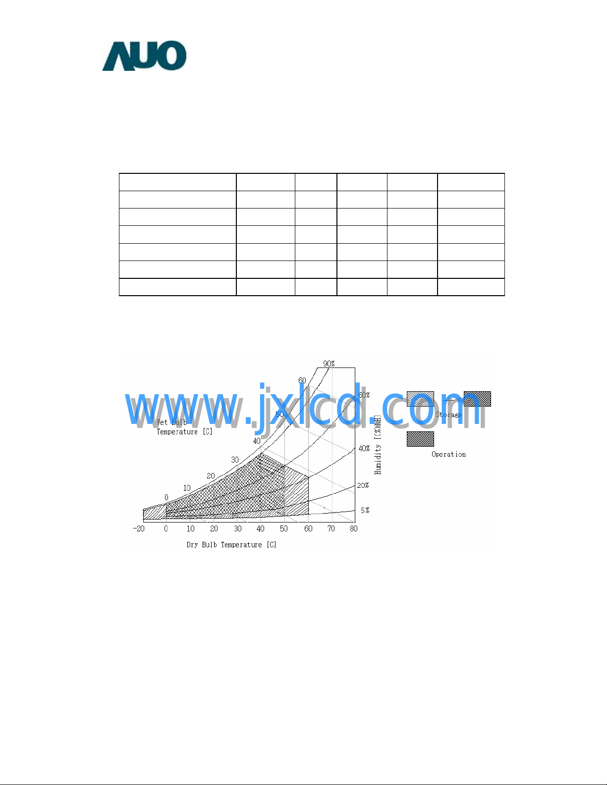
2. Absolute Maximum Ratings
The following are maximum values which, if exceeded, may cause faulty operation or damage to the
unit.
Item Symbol Min Max Unit Note
Logic/LCD Drive Voltage Vdd -0.3 14.0 [Volt] 1
Input Voltage of Signal Vin -0.3 3.6 [Volt] 1
Operating Temperature TOP 0 +50 [
Operating Humidity HOP 10 90 [%RH] 2
Storage Temperature TST -20 +60 [
Storage Humidity HST 10 90 [%RH] 2
Note 1 : Duration = 50msec
Note 2 : Maximum Wet-Bulb should be 39℃ and No condensation.
o
C] 2
o
C] 2
www.jxlcd.com
www.jxlcd.com
©Copyright AU Optronics, Inc.
January, 2007 All Rights Reserved. T230XW01 Ver1.3 7/28
No Reproduction and Redistribution Allowed
Page 8

s
µ
3. Electrical Specification
The T230XW01 requires two power inputs. One is employed to power the LCD electronics and to drive
the TFT array and liquid crystal. An inverter typically generates the second input, which powers the
CCFL.
3-1 Electrical Characteristics
Values Parameter Symbol
Min Typ Max
LCD:
Power Supply Input Voltage Vdd 4.1 5.0 5.9 Vdc
Power Supply Input Current Idd - 590 840 A 1
Power Consumption Pc - 2.95 4.7 Watt 1
Unit Notes
Inrush Current I
Backlight Power Consumption 45.6 50.4 55.2 Watt 2
Total Power Consumption - 54.03 59.52 Watt 2
Life Time 50,000 - Hours 3
The performance of the Lamp in LCM, for example lifetime or brightness, is extremely influenced by
the characteristics of the DC-AC Inverter. So all the parameters of an inverter should be carefully
www.jxlcd.com
www.jxlcd.com
designed so as not to produce too much leakage current from high-voltage output of the inverter.
When you design or order the inverter, please make sure unwanted lighting caused by the mismatch
of the lamp and the inverter (no lighting, flicker, etc) never occurs. When you confirm it, the LCD
Assembly should be operated in the same condition as installed in your instrument.
Do not attach a conducting tape to lamp connecting wire. If the lamp wire attach to conducting tape,
TFT-LCD Module have a low luminance and the inverter has abnormal action because leakage
current occurs between lamp wire and conducting tape.
The relative humidity must not exceed 80% non-condensing at temperatures of 40 ℃ or less. At
temperatures greater than 40℃, the wet bulb temperature must not exceed 39℃. When operate at
low temperatures, the brightness of CCFL will drop and the lifetime of CCFL will be reduced.
Note :
1. Vdd=12.0V, Fv=62Hz, fCLK= 88MHz , 25℃, Vdd Duration time= 470
3 A 1
RUSH
The Power supply input check pattern definition and dissipation reference as below :
Dot pattern:373mA (Max.)
©Copyright AU Optronics, Inc.
January, 2007 All Rights Reserved. T230XW01 Ver1.3 8/28
No Reproduction and Redistribution Allowed
Page 9

White pattern:290m A
Black pattern:345m A
1366*768*3 Pixel
Dot pattern (Dot)
1366*768*3 Pixel
Gray Level 255 (White Screen)
Pixel Gray Level 0
RGBRGBRGBRGBRGBRGB
Pixel Gray Level 255
RGBRGBRGBRGBRGBRGB
Pixel Gray Level 255
RGBRGBRGBRGBRGBRGB
Pixel Gray Level 0
www.jxlcd.com
www.jxlcd.com
Vertical gray scale pattern:311m A(Typ.)
2. The lamp power consumption shown above does include loss of external inverter at 25 ℃..
3. The life is determined as the time at which luminance of the lamp is 50% compared to that of
initial value at the typical lamp current on condition of continuous operating at 25 ±2℃.
1366*768*3 Pixel
Gray Level 0 (Black Screen)
1366*768*3 Pixel
Vertical Gray Scale
R/G/B Level 0~Level 255 Vertical
Grey Scale pattern
©Copyright AU Optronics, Inc.
January, 2007 All Rights Reserved. T230XW01 Ver1.3 9/28
No Reproduction and Redistribution Allowed
Page 10

3-2 Interface Connections
- LCD connector (CN1): JAE FI-E30S or equivalent
- LVDS Transmitter: DS90C385 (NS) or equivalent
Note:
1. All GND (ground) pins should be connected together and should also be connected to the
LCD’s metal frame. All Vdd (power input) pins should be connected together.
Pin No Symbol Description Note
1
2
3
4 GND Ground
5 Rx0- LVDS Channel 0 [Polarity: Negative]
6 Rx0+ LVDS Channel 0 [Polarity: Positive]
7 GND Ground
8 Rx1- LVDS Channel 1 [Polarity: Negative]
9 Rx1+ LVDS Channel 1 [Polarity: Positive]
10 GND Ground
11 Rx2- LVDS Channel 2 [Polarity: Negative]
12 Rx2+ LVDS Channel 2 [Polarity: Positive]
13 GND Ground
www.jxlcd.com
www.jxlcd.com
14 RXCLK- LVDS Clock [Polarity: Negative]
15 RXCLK+ LVDS Clock [Polarity: Positive]
16 GND Ground
17 Rx3- LVDS Channel 3 [Polarity: Negative]
18 Rx3+ LVDS Channel 3 [Polarity: Positive]
19 GND Ground
20
21 LVDS Option* Low for JEIDA, High/Open for NS
22
23 GND Ground
24 GND Ground
25 GND Ground
26 Vdd (+5V) 5V, DC, Regulated
27 Vdd (+5V) 5V, DC, Regulated
28 Vdd (+5V) 5V, DC, Regulated
29 Vdd (+5V) 5V, DC, Regulated
30 Vdd (+5V) 5V, DC, Regulated
N.C. No Connection ( Auo internal Test Pin)
N.C. No Connection ( Auo internal Test Pin)
N.C. No Connection ( Auo internal Test Pin)
N.C. No Connection ( Auo internal Test Pin)
N.C. No Connection ( Auo internal Test Pin)
©Copyright AU Optronics, Inc.
January, 2007 All Rights Reserved. T230XW01 Ver1.3 10/28
No Reproduction and Redistribution Allowed
Page 11

u LVDS Option = L (GND)
Previous Cycle Current Cycle Next Cycle
RINCLK+
Clock
RINCLK-
RIN0+
RIN0-
RIN1+
RIN1-
RIN2+
RIN2-
RIN3+
RIN3-
G7
R2R7 G2G2R2R3 R4R5R6 R3
G3B2 B3B3G3G4 G5G6 G4
B4NA DEDEB4B5 B6B7NA B5
R0B1 NANAR0R1 G0G1B0 R1
u LVDS Option = H (3.3V) / Open
Previous Cycle Current Cycle Next Cycle
RINCLK+
www.jxlcd.com
Clock
www.jxlcd.com
RINCLK-
RIN0+
RIN0-
R0R5 G0G0R0R1 R2R3R4 R1
RIN1+
RIN1-
RIN2+
RIN2-
RIN3+
RIN3-
G1B0 B1B1G1G2 G3G4G5 G2
B2NA DEDEB2B3 B4B5NA
B3
R6B7 NANAR6R7 G6G7B6 R7
©Copyright AU Optronics, Inc.
January, 2007 All Rights Reserved. T230XW01 Ver1.3 11/28
No Reproduction and Redistribution Allowed
Page 12

Backlight Connector Pin Configuration
1. Electrical specification
Item Symb. Condition
Min Typ Max
Input Voltage VDDB - 21.6 24 26.4 VDC
Input Current IDDB VDDB=24V 1.9 2.1 2.3 ADC 1
Input Power PDDB VDDB=24V 45.6 50.4 55.2 W 1
Inrush Current IRUSH VDDB=24V - - 3.15 ADC 1,2
Spec
Units Note.
On/Off Control Voltage VBLON
On/Off Control Current
Dimming Control
VDIM
Voltage
Note1. VDIM = 3.3V (Ta = 25+-5℃, Turn on for 45 minutes)
Note2. Measurement condition rising time = 20ms (VDD: 10%~90%)
ON VDDB=24V 2 - 5.25
OFF VDDB=24V 0 - 0.8
IBLON VDDB=24V 0 - 1.5 mADC
MAX VDDB=24V - 3.3 - 1
MIN VDDB=24V - 0 -
2. Inverter Pin Assignment
Connector (CN1):JST_S14B-PH-SM3-TB or equivalent
Pin No.
1 VDDB Operation Voltage Supply, +24V DC regulated 24V
2 VDDB Operation Voltage Supply, +24V DC regulated 24V
3 VDDB Operation Voltage Supply, +24V DC regulated 24V
www.jxlcd.com
www.jxlcd.com
4 VDDB Operation Voltage Supply, +24V DC regulated 24V
5 VDDB Operation Voltage Supply, +24V DC regulated 24V
6 GND Ground and Current Return GND
7 GND Ground and Current Return GND
8 GND Ground and Current Return GND
Symbol Description Default
VDC
VDC
9 GND Ground and Current Return GND
10 GND Ground and Current Return GND
11 N.C This pin is floating inside ; N.C
12 VBLON BL On-Off: Open/High (3.3V) for BL On as default On
13 PDIM Internal PWM ; 0V (GND) min Lum / 3.3V (open)Max Lum 100%
14 N.C This pin is floating inside ; N.C
©Copyright AU Optronics, Inc.
January, 2007 All Rights Reserved. T230XW01 Ver1.3 12/28
No Reproduction and Redistribution Allowed
Page 13

3-3 Signal Timing Specifications
This is the signal timing required at the input of the User connector. All of the interface signal
timing should be satisfied with the following specifications for it’s proper operation.
* Timing Table
Signal Item Symbol Min Type Max Unit
Period Tv 784 806 1063 Th
Active Tdisp (v) — 768 — Th
Vertical Section
Horizontal Section
Blanking Tblk (v) 16 38 295 Th
Period Th 1434 1560 2000 Tclk
Active Tdisp (h) — 1366 — Tclk
Blanking Tblk (h) 68 194 634 Tclk
Clock
Vertical Frequency Frequency
Horizontal Frequency Frequency
1.) Display position is specific by the rise of DE signal only.
Horizontal display position is specified by the rising edge of 1st DCLK after the rise of 1st DE, is
displayed on the left edge of the screen.
Vertical display position is specified by the rise of DE after a “Low” level period equivalent to eight
www.jxlcd.com
www.jxlcd.com
times of horizontal period. The 1st data corresponding to one horizontal line after the rise the of 1st DE
is displayed at the top line of screen.
3.) If a period of DE “High” is less than 1366 DCLK or less than 768 lines, the rest of the screen
displays black.
4.) The display position does not fit to the screen if a period of DE “High” and the effective data period
do not synchronize with each other.
Period Tclk 11.36 13.16 18.19 ns
Frequency Freq 55 76 85 MHz
Vs 48 60 75 Hz
Hs 39.45 61.65 KHz
©Copyright AU Optronics, Inc.
January, 2007 All Rights Reserved. T230XW01 Ver1.3 13/28
No Reproduction and Redistribution Allowed
Page 14

3-4 Signal Timing Waveforms
www.jxlcd.com
www.jxlcd.com
©Copyright AU Optronics, Inc.
January, 2007 All Rights Reserved. T230XW01 Ver1.3 14/28
No Reproduction and Redistribution Allowed
Page 15

1 1 1 1 1 1 1 0 0 0 0 0 0 0 0 0 0 0 0 0 0 0 0
0 0 0 0 0 0 0 0 0 0 0 0 0 0 0 1 1 1 1 1 1 1 1
0 0 0 0 0 0 0 1 1 1 1 1 1 1 1 1 1 1 1 1 1 1 1
0 0 0 0 0 0 0 0 0 0 0 0 0 0 0 0 0 0 0 0 0 0 0
0 0 0 0 0 0 1 0 0 0 0 0 0 0 0 0 0 0 0 0 0 0 0
1 1 1 1 1 1 0 0 0 0 0 0 0 0 0 0 0 0 0 0 0 0 0
1 1 1 1 1 1 1 0 0 0 0 0 0 0 0 0 0 0 0 0 0 0 0
0 0 0 0 0 0 0 0 0 0 0 0 0 0 0 0 0 0 0 0 0 0 0
0 0 0 0 0 0 0 0 0 0 0 0 0 0 0 0 0 0 0 0 0 0 1
0 0 0 0 0 0 0 0 0 0 0 0 0 0 0 1 1 1 1 1 1 1 0
0 0 0 0 0 0 0 0 0 0 0 0 0 0 0 1 1 1 1 1 1 1 1
3-5 Color Input Data Reference
The brightness of each primary color (red, green and blue) is based on the 8 bit gray scale data input
for the color; the higher the binary input, the brighter the color. The table below provides a reference for
color versus data input.
COLOR DATA REFERENCE
Color
Basic
Color
RED
Input Color Data
RED
MSB
LSB
R7 R6 R5 R4 R3 R2 R1 R0 G7 G6 G5 G4 G3 G2 G1 G0 B7 B6 B5 B4 B3 B2 B1 B0
Black(L0) 0 0 0 0 0 0 0 0 0 0 0 0 0 0 0 0 0 0 0 0 0 0 0 0
Red 1
Green 0 0 0 0 0 0 0 0 1 1 1 1 1 1 1 1 0 0 0 0 0 0 0 0
Blue 0
Cyan 0
Magenta 1 1 1 1 1 1 1 1 0 0 0 0 0 0 0 0 1 1 1 1 1 1 1 1
Yellow 1 1 1 1 1 1 1 1 1 1 1 1 1 1 1 1 0 0 0 0 0 0 0 0
www.jxlcd.com
www.jxlcd.com
White(L255) 1 1 1 1 1 1 1 1 1 1 1 1 1 1 1 1 1 1 1 1 1 1 1 1
RED 0
RED 0
---RED 1
MSB LSB
GREEN
BLUE
MSB
LSB
RED 1
GREEN
BLUE
©Copyright AU Optronics, Inc.
January, 2007 All Rights Reserved. T230XW01 Ver1.3 15/28
No Reproduction and Redistribution Allowed
GREEN 0 0 0 0 0 0 0 0 0 0 0 0 0 0 0 0 0 0 0 0 0 0 0 0
GREEN 0 0 0 0 0 0 0 0 0 0 0 0 0 0 0 1 0 0 0 0 0 0 0 0
---GREEN 0 0 0 0 0 0 0 0 1 1 1 1 1 1 1 0 0 0 0 0 0 0 0 0
GREEN) 0 0 0 0 0 0 0 0 1 1 1 1 1 1 1 1 0 0 0 0 0 0 0 0
BLUE 0
BLUE 0
------BLUE 0
BLUE 0
Page 16

3-6 Power Sequence
3.6.1 Power Sequence for LCD
Power Supply for LCD
(Vdd)
LVDS Data & CLK
Power for LAMP
Values
Parameter
www.jxlcd.com
www.jxlcd.com
t1 0.47 - 20 ms
t2 20 - 50 ms
t3 200 - - ms
t4 10 - - ms
t5 1 - 50 ms
t6 - - 300 ms
t7 1000 - - ms
Apply the lamp voltage within the LCD operating range. When the backlight turns on before the LCD
operation or the LCD turns off before the backlight turns off, the display may momentarily become
abnormal.
Caution : The above on/off sequence should be applied to avoid abnormal function in the display. In
Min. Typ. Max.
Units
case of handling, make sure to turn off the power when you plug the cable into the input connector or
pull the cable out of the connector.
©Copyright AU Optronics, Inc.
January, 2007 All Rights Reserved. T230XW01 Ver1.3 16/28
No Reproduction and Redistribution Allowed
Page 17

3.6.2 Power Sequence for Inverter
www.jxlcd.com
www.jxlcd.com
Values Parameter
Min. Typ. Max.
T1 20 - - ms
T2 50 - - ms
T3 50 - - ms
T4 50 - - ms
T5 0 - - ms
T6 - - 10 ms
Units
©Copyright AU Optronics, Inc.
January, 2007 All Rights Reserved. T230XW01 Ver1.3 17/28
No Reproduction and Redistribution Allowed
Page 18

4. Optical Specification
Optical characteristics are determined after the unit has been ‘ON’ and stable for approximately 30 minutes
in a dark environment at 25℃. The values specified are at an approximate distance 50cm from the LCD
surface at a viewing angle of Φ and θequal to 0°.
PR880 or equivalent
Fig.4-1 Optical measurement equipment and method
Parameter
Contrast Ratio CR 550 700 1
Surface Luminance, white LWH 360 450
Luminance Variation
Response Time
Rise Time Tr 7 13 ms
www.jxlcd.com
Decay Time
Color Coordinates
Viewing Angle by ELDIM
www.jxlcd.com
RED R
R
GREEN G
G
BLUE B
B
WHITE W
W
Symbol
Min. Typ. Max.
δ
WHITE
9 p 1.25 3
Tγ
Tf 1 3 ms
0.638
X
0.337
Y
0.299
X
0.604
Y
0.145
X
0.059
Y
X
Y
Typ.-0.03
0.280
Values
8 16 ms 4,5 (Tr+Tf)
Typ.+0.03
0.292
Units Notes
cd/㎡
2
Contrast Ratio >10
x axis, right(φ=0°) θr
x axis, left(φ=180°) θl
y axis, up(φ=90°) θu
y axis, down (φ=0°) θd
©Copyright AU Optronics, Inc.
January, 2007 All Rights Reserved. T230XW01 Ver1.3 18/28
No Reproduction and Redistribution Allowed
65 80 Degree 6
65 80
65 80
65 80
Page 19

Contrast ratio (CR)=
Brightness on the
white (L255
) state
Brightness on the black
(L0
) state
Note:
1. Contrast Ratio (CR) is defined mathematically as:
2. Surface luminance is luminance value at point 1 across the LCD surface 50cm from the surface with
all pixels displaying white. From more information see FIG 4-2. When IBL = 6.5mA, LWH=450cd/㎡
(typ.) LWH=Lon1, Where Lon1 is the luminance with all pixels displaying white at center 1 location.
H
V/2
V/6
Fig.4-2 Optical measurement point
3. The variation in surface luminance, δWHITE is defined (center of Screen) as:
www.jxlcd.com
www.jxlcd.com
δ
WHITE(9P)
=Maximum(L
on1
, L
on2
,…,L
)/Minimum(L
on9
1
H/2 H/6
, L
on1
on2
,…L
on9
)
4. Response time is the time required for the display to transition from white(L255) to black(L0) (Decay
Time, TrD=Tf ) and from black(L0) to white(L255) (Rise Time, TrR=Tr ). The response time interval is
between the 10% and 90% of 1st frame amplitudes. For additional information see FIG 4-3.
TrD
TrR
V
©Copyright AU Optronics, Inc.
January, 2007 All Rights Reserved. T230XW01 Ver1.3 19/28
No Reproduction and Redistribution Allowed
Fig.4-3 Response time
Page 20

5. Viewing angle is the angle at which the contrast ratio is greater than 10. The angles are
determined for the horizontal or x axis and the vertical or y axis with respect to the z axis which is
normal to the LCD surface. For more information see FIG 4-5.
6. To be measured with a viewing cone of 1°by Topcon luminance meter ELDIM EZ Contrast 160D.
Fig.4-5 Viewing Angle Definition
www.jxlcd.com
www.jxlcd.com
©Copyright AU Optronics, Inc.
January, 2007 All Rights Reserved. T230XW01 Ver1.3 20/28
No Reproduction and Redistribution Allowed
Page 21

5. Mechanical Characteristics
The contents provide general mechanical characteristics for the model T230XW01. In addition the
figures in the next page are detailed mechanical drawing of the LCD.
Outline Dimension
Weight 3300g (typ.)
Surface Treatment HC, 3H
www.jxlcd.com
www.jxlcd.com
Horizontal (typ.) 546.0mm
Vertical (typ.) 318.3mm
Depth (typ.) 46.0mm(Max.)
Horizontal (typ.) 512.2mm Bezel Area
Vertical (typ.) 289.8mm
Horizontal 508.152mm Active Display Area
Vertical 285.696mm
©Copyright AU Optronics, Inc.
January, 2007 All Rights Reserved. T230XW01 Ver1.3 21/28
No Reproduction and Redistribution Allowed
Page 22

Front View:
www.jxlcd.com
www.jxlcd.com
©Copyright AU Optronics, Inc.
January, 2007 All Rights Reserved. T230XW01 Ver1.3 22/28
No Reproduction and Redistribution Allowed
Page 23

Rear View:
www.jxlcd.com
www.jxlcd.com
©Copyright AU Optronics, Inc.
January, 2007 All Rights Reserved. T230XW01 Ver1.3 23/28
No Reproduction and Redistribution Allowed
Page 24

6. International Standard
6-1. Safety
(1) UL6500, Underwriters Laboratories, Inc. (AUO file number : E204356)
Standard for Safety of Information Technology Equipment Including electrical Business
Equipment.
(2) CAN/CSA C22.2 No. 950-95 Third Edition, Canadian Standards Association, Jan. 28, 1995
Standard for Safety of Information Technology Equipment Including Electrical Business
Equipment.
(3) EN60950 : 1992+A2: 1993+A2: 1993+C3: 1995+A4: 1997+A11: 1997
IEC 950: 1991+A1: 1992+A2: 1993+C3: 1995+A4:1996
IEC 60065
European Committee for Electro technical Standardization (CENELEC)
EUROPEAN STANDARD for Safety of Information Technology Equipment Including Electrical
Business Equipment.
6-2. EMC
a) ANSI C63.4 “Methods of Measurement of Radio-Noise Emissions from Low-Voltage Electrical and
Electrical Equipment in the Range of 9kHz to 40GHz. “American National standards
Institute(ANSI), 1992
b) C.I.S.P.R “Limits and Methods of Measurement of Radio Interface Characteristics of Information
www.jxlcd.com
www.jxlcd.com
Technology Equipment.” International Special committee on Radio Interference.
c) EN 55022 “Limits and Methods of Measurement of Radio Interface Characteristics of Information
Technology Equipment.” European Committee for Electrotechnical Standardization. (CENELEC),
1998
©Copyright AU Optronics, Inc.
January, 2007 All Rights Reserved. T230XW01 Ver1.3 24/28
No Reproduction and Redistribution Allowed
Page 25

AU
O
7. Packing
Label Sample
Green Mark Description:
For Pb Free products, AUO will add for identification.
For RoHS compatible products, AUO will add for identification.
Note. The Green Mark will be present only when the green documents have been ready by AUO
Internal Green Team. (The definition of green design follows the AUO green design checklist .)
Carton Label
ptronics
QTY: 5
www.jxlcd.com
www.jxlcd.com
MODEL NO: T230XW01 VX
PART NO: 97.23T01.XXX
CUSTOMER NO:
CARTON NO:
Made in Taiwan
*PM100-01A1600001*
Packing size:
Carton Box: 370mm(W)x400mm(L)x655mm(H)
Pallet Size: 1140mm(W)*820mm(L)*123mm(H)
Shipping volume per pallet:
By Air: (3*2)*2 layers,
one pallet put 12 boxes,
total 60ps module.
By Sea: (3*2)*3 layers,
one pallet put 18 boxes,
total 90ps module.
©Copyright AU Optronics, Inc.
January, 2007 All Rights Reserved. T230XW01 Ver1.3 25/28
No Reproduction and Redistribution Allowed
Page 26

Packing process
www.jxlcd.com
www.jxlcd.com
©Copyright AU Optronics, Inc.
January, 2007 All Rights Reserved. T230XW01 Ver1.3 26/28
No Reproduction and Redistribution Allowed
Page 27

8. PRECAUTIONS
Please pay attention to the followings when you use this TFT LCD module.
8-1 MOUNTING PRECAUTIONS
(1) You must mount a module using holes arranged in four corners or four sides.
(2) You should consider the mounting structure so that uneven force (ex. Twisted stress) is not
applied to module. And the case on which a module is mounted should have sufficient strength so
that external force is not transmitted directly to the module.
(3) Please attach the surface transparent protective plate to the surface in order to protect the
polarizer. Transparent protective plate should have sufficient strength in order to the resist external
force.
(4) You should adopt radiation structure to satisfy the temperature specification.
(5) Acetic acid type and chlorine type materials for the cover case are not desirable because the
former generates corrosive gas of attacking the polarizer at high temperature and the latter causes
circuit break by electro-chemical reaction.
(6) Do not touch, push or rub the exposed polarizers with glass, tweezers or anything harder than
HB pencil lead. And please do not rub with dust clothes with chemical treatment. Do not touch the
surface of polarizer for bare hand or greasy cloth. (Some cosmetics are detrimental to the
polarizer.)
www.jxlcd.com
www.jxlcd.com
(7) When the surface becomes dusty, please wipe gently with absorbent cotton or other soft
materials like chamois soaks with petroleum benzene. Normal-hexane is recommended for
cleaning the adhesives used to attach front/ rear polarizers. Do not use acetone, toluene and
alcohol because they cause chemical damage to the polarizer.
(8) Wipe off saliva or water drops as soon as possible. Their long time contact with polarizer
causes deformations and color fading.
(9) Do not open the case because inside circuits do not have sufficient strength.
8-2 OPERATING PRECAUTIONS
(1) The spike noise causes the mis-operation of circuits. It should be lower than following
voltage: V=±200mV(Over and under shoot voltage)
(2) Response time depends on the temperature. (In lower temperature, it becomes
longer..)
(3) Brightness depends on the temperature. (In lower temperature, it becomes lower.) And
in lower temperature, response time (required time that brightness is stable after turned
on) becomes longer.
©Copyright AU Optronics, Inc.
January, 2007 All Rights Reserved. T230XW01 Ver1.3 27/28
No Reproduction and Redistribution Allowed
Page 28

(4) Be careful for condensation at sudden temperature change. Condensation makes
damage to polarizer or electrical contacted parts. And after fading condensation, smear
or spot will occur.
(5) When fixed patterns are displayed for a long time, remnant image is likely to occur.
(6) Module has high frequency circuits. Sufficient suppression to the electromagnetic
interference shall be done by system manufacturers. Grounding and shielding methods
may be important to minimize the interface.
8-3 ELECTROSTATIC DISCHARGE CONTROL
Since a module is composed of electronic circuits, it is not strong to electrostatic discharge. Make
certain that treatment persons are connected to ground through wrist band etc. And don ’t touch
interface pin directly.
8-4 PRECAUTIONS FOR STRONG LIGHT EXPOSURE
Strong light exposure causes degradation of polarizer and color filter.
8-5 STORAGE
When storing modules as spares for a long time, the following precautions are necessary.
(1) Store them in a dark place. Do not expose the module to sunlight or fluorescent light. Keep the
temperature between 5℃ and 35℃ at normal humidity.
www.jxlcd.com
www.jxlcd.com
(2) The polarizer surface should not come in contact with any other object. It is recommended that
they be stored in the container in which they were shipped.
8-6 HANDLING PRECAUTIONS FOR PROTECTION FILM
(1) The protection film is attached to the bezel with a small masking tape. When the protection film is
peeled off, static electricity is generated between the film and polarizer. This should be peeled off
slowly and carefully by people who are electrically grounded and with well ion-blown equipment or
in such a condition, etc.
(2) When the module with protection film attached is stored for a long time, sometimes there remains
a very small amount of flue still on the Bezel after the protection film is peeled off.
(3) You can remove the glue easily. When the glue remains on the Bezel or its vestige is recognized,
please wipe them off with absorbent cotton waste or other soft material like chamois soaked with
normal-hexane.
©Copyright AU Optronics, Inc.
January, 2007 All Rights Reserved. T230XW01 Ver1.3 28/28
No Reproduction and Redistribution Allowed
 Loading...