

Page 1

Product Specification
M230UW01 V.1
AU OPTRONICS CORPORATION
Product Specification
23.0” Wide-UXGA Color TFT-LCD Module
Model Name: M230UW01 V.1
Approved by Prepared by
www.jxlcd.com
www.jxlcd.com
CC Chiu GaryChen
DDBU Marketing Division / AU Optronics corporation
Customer Checked & Approved by
Ver0.1
1
Page 2

Product Specification
M230UW01 V.1
) Preliminary Specifications
Product Specification
23.0” Wide-UXGA Color TFT-LCD Module
Model Name: M230UW01
V.1
(u
( ) Final Specifications
Note: This Specification is subject to change without notice.
www.jxlcd.com
www.jxlcd.com
Ver0.1
2
Page 3

Product Specification
M230UW01 V.1
Contents
1.0 Handling Precautions.............................................................5
2.0 General Description...............................................................6
2.1 Display Characteristics.......................................................................................................6
2.2 Optical Characteristics.......................................................................................................7
3.0 Functional Block Diagram....................................................10
4.0 Absolute Maximum Ratings..................................................11
4.1 TFT LCD Module..............................................................................................................11
4.2 Backlight Unit...................................................................................................................11
4.3 Absolute Ratings of Environment (TETANTIVE)..............................................................11
5.0 Electrical characteristics......................................................12
5.1 TFT LCD Module..............................................................................................................12
5.1.1 Power Specification...............................................................................................12
5.1.2 Signal Electrical Characteristics..............................................................................13
5.2 Inverter Electrical Characteristics.....................................................................................14
6.0 Signal Characteristic............................................................15
6.1 Pixel Format Image..........................................................................................................15
6.2 The input data format.......................................................................................................15
6.3 Signal Description............................................................................................................16
6.4 Interface Timing................................................................................................................17
6.4.1 Timing Characteristics...........................................................................................17
6.4.2 Timing diagram....................................................................................................18
6.5 Power ON/OFF Sequence................................................................................................19
www.jxlcd.com
www.jxlcd.com
7.0 Connector & Pin Assignment................................................20
7.1 TFT LCD Module..............................................................................................................20
7.2 Backlight Unit...................................................................................................................20
8.0 Reliability............................................................................21
9.0 Safety..................................................................................21
9.1 Sharp Edge Requirements...............................................................................................21
9.2 Materials...........................................................................................................................21
9.2.1 Toxicity...............................................................................................................21
9.3 Capacitors........................................................................................................................21
10.0 Other requirement.............................................................22
10.1 National Test Lab Requirement......................................................................................22
10.2 Label..............................................................................................................................22
13.0 Mechanical Characteristics.................................................23
Ver0.1
9.2.2 Flammability........................................................................................................21
3
Page 4

Product Specification
M230UW01 V.1
Record of Revision
Version and Date Page
0.1 2004/12/27 All First Edition for Customer All
www.jxlcd.com
www.jxlcd.com
Old description New Description Remark
Ver0.1
4
Page 5

Product Specification
M230UW01 V.1
1.0 Handling Precautions
1) Since front polarizer is easily damaged, pay attention not to scratch it.
2) Be sure to turn off power supply when inserting or disconnecting from input connector.
3) Wipe off water drop immediately. Long contact with water may cause discoloration or spots.
4) When the panel surface is soiled, wipe it with absorbent cotton or other soft cloth.
5) Since the panel is made of glass, it may break or crack if dropped or bumped on hard surface.
6) Since CMOS LSI is used in this module, take care of static electricity and insure human earth when
handling.
7) Do not open nor modify the Module Assembly.
8) Do not press the reflector sheet at the back of the module to any directions.
9) In case if a module has to be put back into the packing container slot after once it was taken out from
the container, do not press the center of the CCFL reflector edge. Instead, press at the far ends of the
CCFL reflector edge softly. Otherwise the TFT module may be damaged.
10) At the insertion or removal of the Signal Interface Connector, be sure not to rotate nor tilt the Interface
Connector of the TFT module.
11) After installation of the TFT module into an enclosure (Desktop monitor Bezel, for example), do not
twist nor bend the TFT Module even momentary. At designing the enclosure, it should be taken into
consideration that no bending/twisting forces are applied to the TFT module from outside. Otherwise
the TFT module may be damaged.
www.jxlcd.com
www.jxlcd.com
Ver0.1
5
Page 6

Product Specification
M230UW01 V.1
2.0 General Description
This specification applies to the 23.0 inch Color TFT-LCD Module M230UW01.
The display supports the WUXGA (1920(H) x 1200(V)) screen format and 16.7M colors (RGB 8-bits data).
All input signals are 2 Channel LVDS interface compatible.
This module contains an inverter card for backlight.
2.1 Display Characteristics
The following items are characteristics summary on the table under 25 ℃ condition:
ITEMS Unit SPECIFICATIONS
Screen Diagonal [mm] 584.15 (23")
Active Area [mm] 495.36 (H) x 309.6 (V)
Pixels H x V 1920(x3) x 1200
Pixel Pitch [mm] 0.258 (per one triad) x 0.258
Pixel Arrangement R.G.B. Vertical Stripe
Display Mode Normally Black
White Luminance ( Center )
Contrast Ratio 800 : 1 (Typ)
Optical Response Time
(Gray to Gray)
Nominal Input Voltage VDD [Volt] +12.0 V
Power Consumption
(VDD line + Inverter card )
Weight [Grams] 3000 (Max)
Physical Size [mm]
www.jxlcd.com
www.jxlcd.com
Electrical Interface 2 Channel LVDS
Support Color 16.7M colors (RGB 8-bit data )
Surface Treatment
Temperature Range
Operating
Storage (Shipping)
[cd/m2]
[msec] 8 ms (Typ, average)
[Watt]
[oC]
[oC]
250 cd/m
60.0W (Typ.) (inverter V
Min. Typ. Max.
Horizatal(H) 522.4 523.4 523.9
Vertical(V) 335.1 335.6 336.1
Depth(D) 40.5 41.0 41.5
Anti-glare type, Hard Coating (2H)
0 to +50
-20 to +60
2
@
VBR =2.8V (Typ)
=2.8V, all white pattern)
BR
Ver0.1
6
Page 7

Product Specification
M230UW01 V.1
2.2 Optical Characteristics
The optical characteristics are measured under stable conditions at 25℃ and after lighting the B/L 30~40 minutes:
Item Unit Conditions Min. Typ. Max. Note
Note 1
Note 2
Note 3
Note 4
Viewing Angle
Contrast ratio
Response Time
Color / Chromaticity
Coordinates (CIE)
Color Coordinates (CIE) White
White Luminance (central point)
(at inverter VBR =2.8V)
Luminance Uniformity
Crosstalk (in 60Hz)
Flicker
www.jxlcd.com
www.jxlcd.com
[degree]
[degree]
[msec]
[cd/m2]
[%]
[%]
dB
Horizontal (Right)
CR = 10 (Left)
Vertical (Up)
CR = 10 (Down)
Normal Direction
Gray to Gray
(average)
Red x
Red y
Green x
Green y
Blue x
Blue y
White x
White y
75
75
75
75
400 800 -
- 8 12
0.610 0.640 0.670
0.300 0.330 0.360
0.250 0.280 0.310
0.575 0.605 0.635
0.115 0.145 0.175
0.045 0.075 0.105
0.283 0.313 0.343
0.299 0.329 0.359
200 250 -
75 80 -
1.5
-20
85
85
85
85
-
-
-
-
Equipment Pattern Generator, Power Supply, Digital Voltmeter, Luminance meter
(PR 880, BM-5A , BM 7 ,CS-1000, & EZContrast* )
Aperture 1∘with 100cm VD or 2∘with 50cm viewing distance
Test Point Center (VESA point 9)
Environment < 1 lux
*’ EZ Contrast is different measurement tool with very close viewing distance.
LCD Module
PR-880 /
BM5A /
BM7
measuring distance
Module Driving Equipment
Ver0.1
7
Page 8
M230UW01 V.1
9
0 %
Time
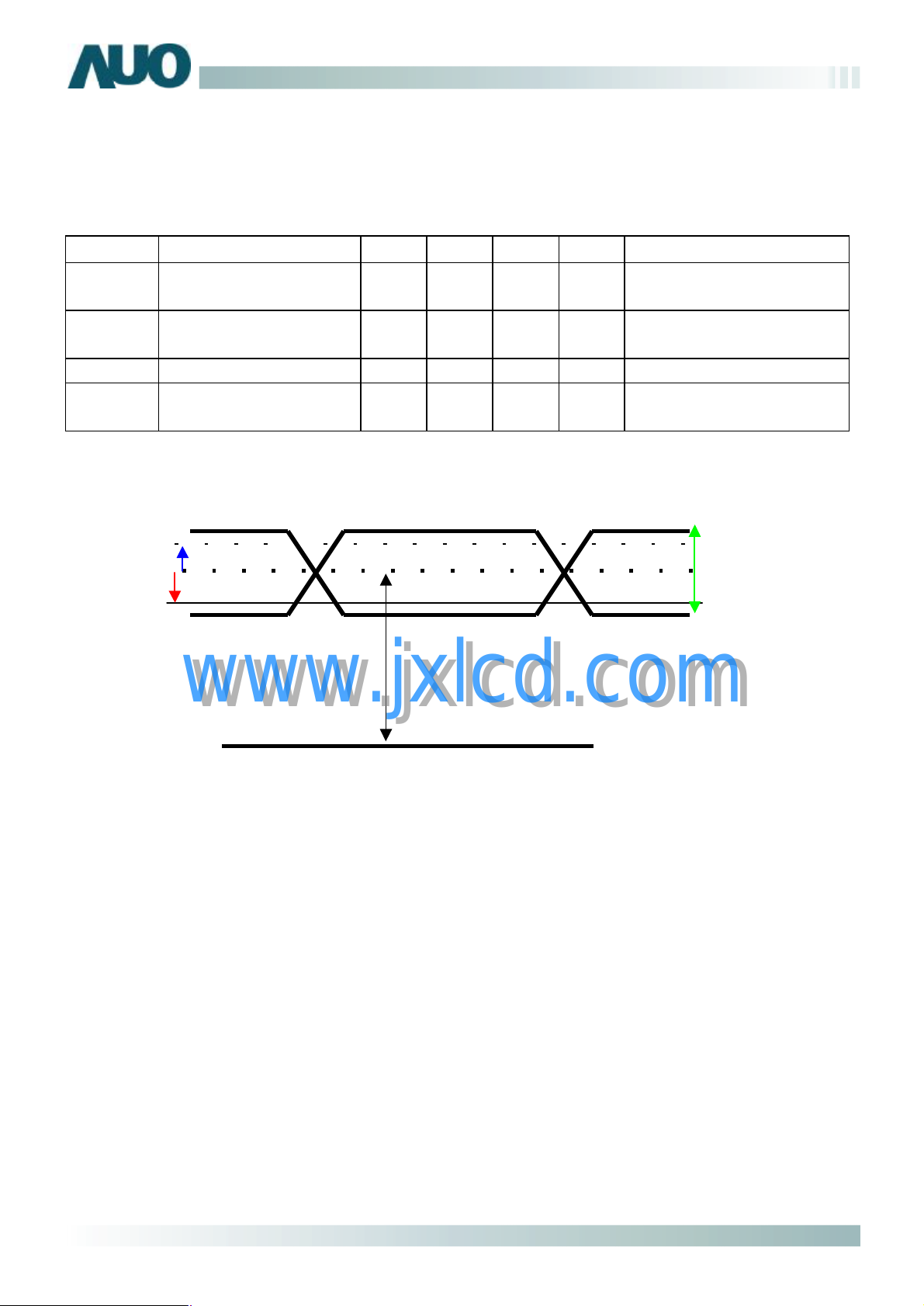
Note 1: The Definition of Response time
B
A
100%
90%
10%
0%
Optical Response Driving Signal
Algorithm:
Product Specification
Time
TrTf
16 B Level - A Level ≥ then the average of Gray-to-Gray response time is 8ms(Typ). At frame rate= 60 Hz
condition.
TrR(On/Off rising time; from “Black” to “White”) + TrF(On/Off falling time; from “White” to “Black”)
= 15 + 5= 20ms(Typ).
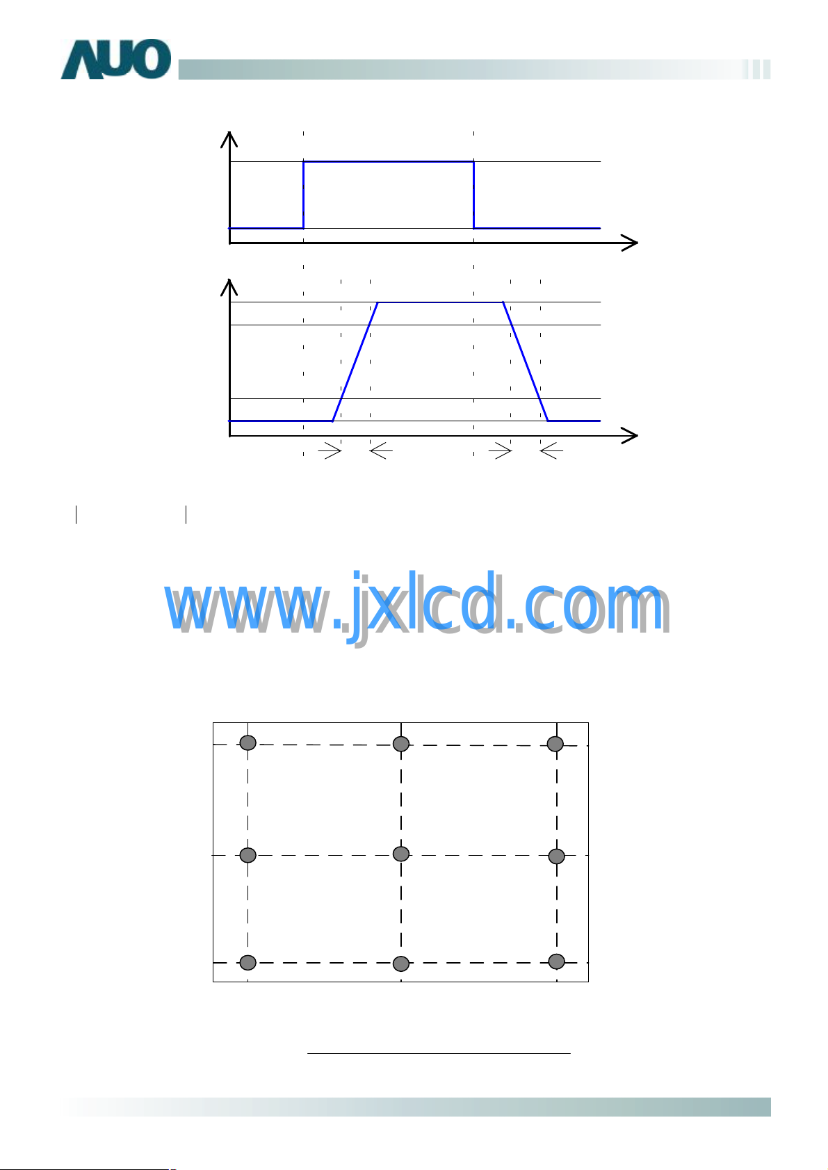
Note 2: Brightness uniformity of these 9 points is defined as below
www.jxlcd.com
www.jxlcd.com
90 %
50 %
10 %
10 %
50 %
Ver0.1
Uniformity =
9)-(1 points 9in Luminance Minimum
9)-(1 Points 9in Luminance Maximum
8
Page 9
Product Specification
M230UW01 V.1
R G B R G B R G B R G B
Level
DC
1/2
1/2
1/6
1/6 A B
1/2
1/2
1/6
1/6
2/3 1/3
1/3 2/3 A’ B’
AC
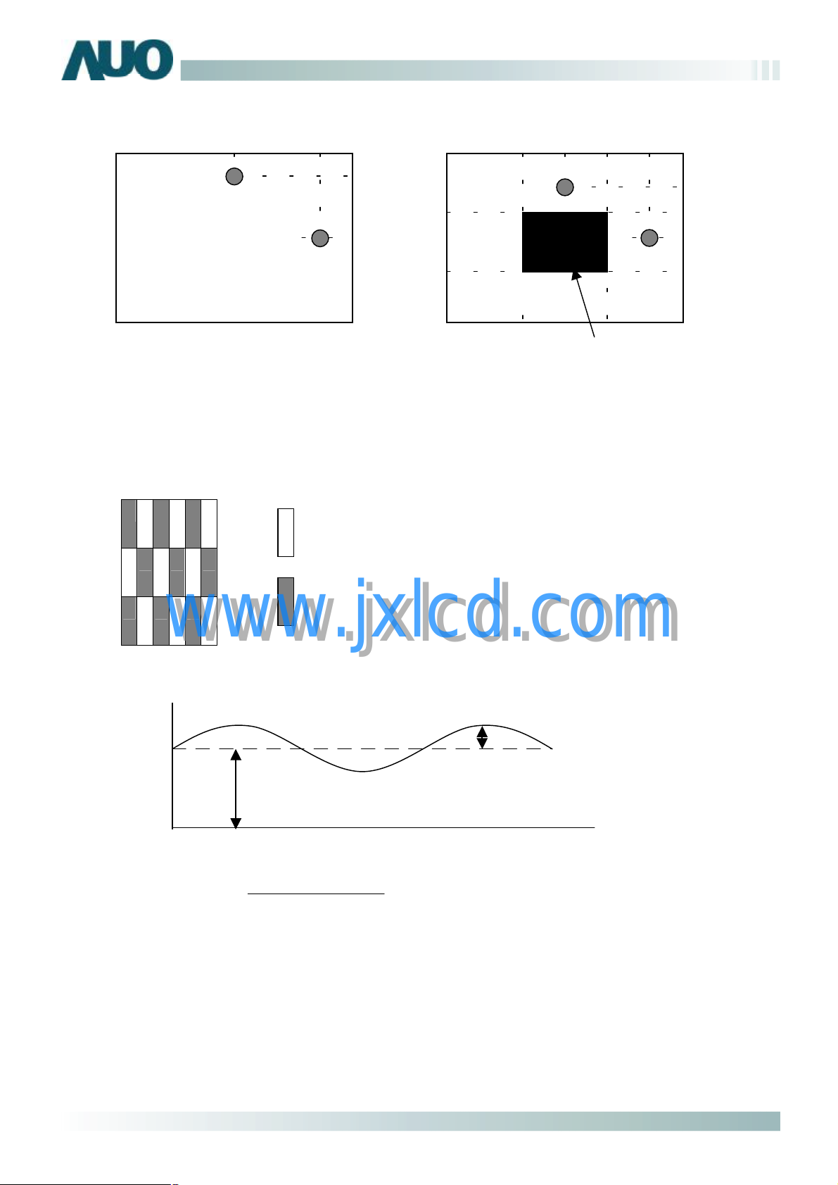
Note 3: Crosstalk is defined as below:
l LA-LA’ l / LA x 100%= 1.5% max., LA and LB are brightness at location A and B
l LB-LB’ l / LB x 100%= 1.5% max., LA’ and LB’ are brightness at location A’ and B’
Note 4: Test Paterm: Subchecker Pattern
184 gray level 184 gray level
Unit: percentage of dimension of display area
0 gray level
R G B R G B
Gray Level = L127
Gray Level = L0
www.jxlcd.com
www.jxlcd.com
Method: Record dBV & DC value with (WESTAR)TRD-100
Amplitude
DC
log20(dB)Flicker =
Hz) 30Level(at AC
Time
Ver0.1
9
Page 10
Product Specification
M230UW01 V.1
+12 V
Connector
Drive
r
Receiver
S
DC
+24V
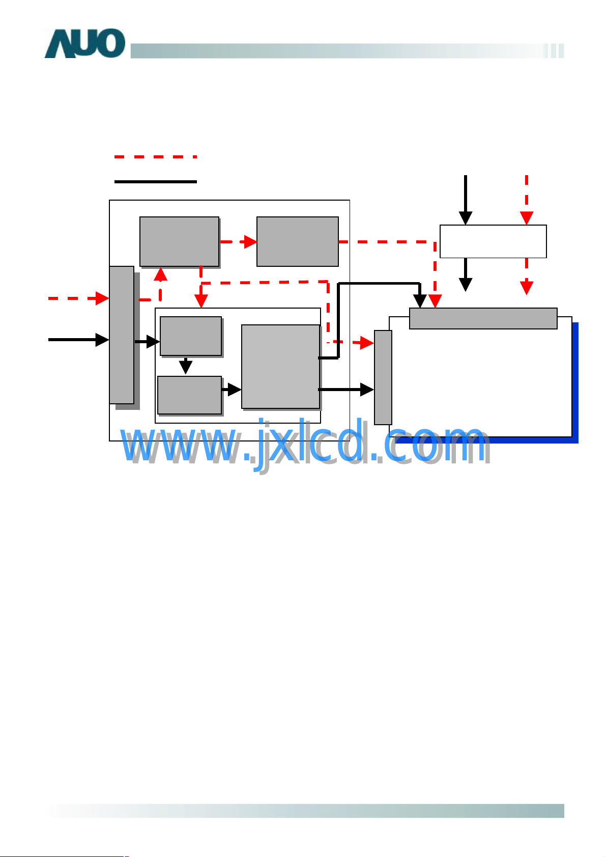
3.0 Functional Block Diagram
The following diagram shows the functional block of the 23.0 inches Color TFT-LCD Module:
2 ch LVD
DC/DC
Converter
Power
Signal
Gamma
Correction
+5V (On/off)
0~3.3V (VBR)
Inverter
AUO ASIC
LVDS
Y-Driver IC
Timing
Controller
Over
www.jxlcd.com
www.jxlcd.com
TFT-LCD 1920(x3) x 1200
pixels
I/F PCB Interface:
JAE or compatible FI-X30SSL-HF (On board Strong type)
Mating Type:
FI-X30HL-T (Locked Type)
FI-X30S-H (Unlocked Type)
Backlight Interface
JST S14B-PH-SM3 or equivalent
Mating Type:
JST PHR-14 or equivalent
Ver0.1
10
Page 11

Product Specification
M230UW01 V.1
I
tem Symbol
Min Max Unit Conditions
Item
Symbol
Min Max Unit Conditions
Item
Symbol
Min Max Unit Conditions
Relative Humidity %
Temperature
℃
-20
0 60 50
95 5
100 0
Operation range
Storage
Storage
80 60 40
20
T=40
℃
,H=95%
T=60
℃
,H=39%
T=50
℃
,H=55%
4.0 Absolute Maximum Ratings
Absolute maximum ratings of the module is as following:
4.1 TFT LCD Module
Logic/LCD Drive
VIN +10.8 +13.2 [Volt] Note 1,2
4.2 Backlight Unit
CCFL Current ICFL 1.5 6 [mA] rms Note 1,2
4.3 Absolute Ratings of Environment (TETANTIVE)
Operating
Operating Humidity HOP 5 95 [%RH]
Storage Temperature TST - 20 60 [
Storage Humidity HST 5 39 [%RH]
Note 1: With in Ta (25℃ )
Note 2: Permanent damage to the device may occur if exceed maximum values
Note 3: For quality perfermance, please refer to AUO IIS(Incoming Inspection Standard).
www.jxlcd.com
www.jxlcd.com
range
TOP 0 50 [
Twb=39℃
range
o
C]
o
C]
Note 3
Ver0.1
11
Page 12
M230UW01 V.1
5.0 Electrical characteristics
5.1 TFT LCD Module
5.1.1 Power Specification
Input power specifications are as follows;
Product Specification
Symbol Parameter Min Typ Max Units
VDD
IDD VDD current - 720 940 [mA]
Irush LCD Inrush Current - - 7.5 [A] Note
PDD VDD Power - 8.65 11.3 [Watt]
VDDrp
Note: Measurement conditions:
Logic/LCD Drive
Voltage
Allowable Logic/LCD
Drive Ripple Voltage
www.jxlcd.com
www.jxlcd.com
11.4 12 12.6 [Volt] ±5%
- - 240
[mV]
p-p
Condition
Vin=12V , All White Pattern,
+30%, at 60Hz
Vin=12V , All White Pattern,
+30%, at 60Hz
Ver0.1
90%
10%
0
1.2 ms
Vin rising time
12.0
12
Page 13
Product Specification
M230UW01 V.1
VID│
VSS
5.1.2 Signal Electrical Characteristics
Input signals shall be low or Hi-Z state when Vin is off
It is recommended to refer the specifications of SN75LVDS82DGG (Texas Instruments) in detail.
Each signal characteristics are as follows;
Symbol Parameter Min Typ Max Units
VTH
VTL
│VID│ Input Differential Voltage 100 600 [mV] Note
VICM
Note: LVDS Signal Waveform
VTH
VTL
Differential Input High
Threshold
Differential Input Low
Threshold
Differential Input Common
Mode Voltage
VICM
www.jxlcd.com
www.jxlcd.com
- - + 100 [mV]
- 100
+1.0 +1.2 +1.5 [V]
- - [mV]
Condition
VICM = 1.2V
Note
VICM = 1.2V
Note
VTH/VTL = ±200mV
Note
│
Ver0.1
13
Page 14

Product Specification
M230UW01 V.1
V
=3.3V
5.2 Inverter Electrical Characteristics
Inverter Symbol Condition
Min. Typ. Max.
Inverter:
Input Voltage V
Input Current I
Input Power P
Brightness Adjust VBR 0 2.8 3.3 V 3
B/L on/off control V
Input inrush current I
Lamp:
Life time V
Notes:
1. The input voltage ripple is limited below 400mVp-p.
2. The specified current and power consumption are under the typical supply input voltage, 24V.
www.jxlcd.com
3. ICFL = 5mA when VBR =2.8V, and ICFL= 5.5mA when VBR =3.3V.
4. Test condition: V
current within V
www.jxlcd.com
DDB
DDB
22.0 24.0 26.0 V 1
DDB
VBR =2.8V 1.8 2.1 2.4 A 2
DDB
VBR =2.8V 45.0 50.4 56.0 Watt 2
B
ON/OFF
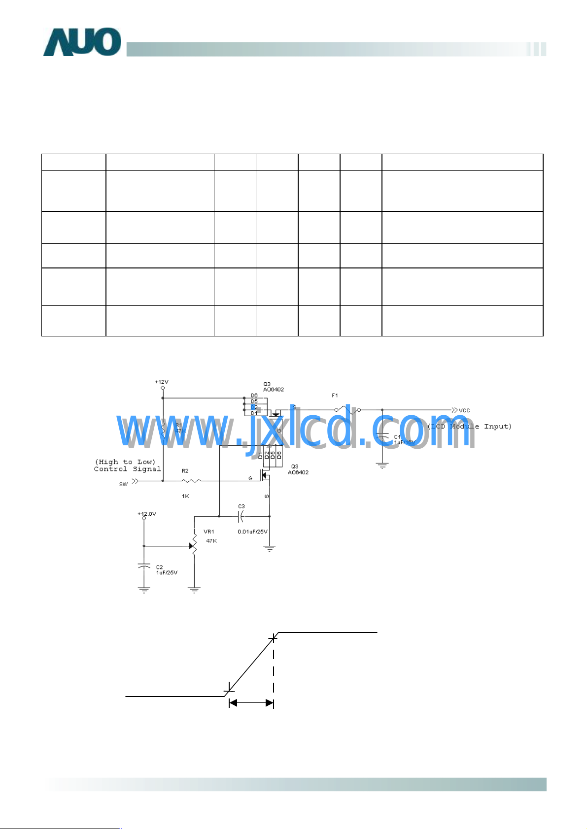
INRUSH
rising time is 10ms. The test schematic as follow. Calculate the inverter input inrush
rising time.
Lamp ON = 4.0 - 5.0 V
Lamp OFF = 0 - 0.8 V
V
=24V,
DDB
=2.8V 50,000 - - Hrs 5
BR
- - 3.5 A 4
Values
Unit Notes
5. The life is determined as the time at which luminace of the lamp is 50% compared to that of initial value at the
typical lamp current on condition of continuous operating at 25±2C
6. Electrical charecteristics are determined after the unit has been ‘ON’ and stable for approximately 30min at
25±2C.
Ver0.1
14
Page 15

Product Specification
M230UW01 V.1
R G B R G B R G B R G B R G B R G B R G B R G B
1 2 1
919 192
0 1st Line
1200
Line
6.0 Signal Characteristic
6.1 Pixel Format Image
Following figure shows the relationship of the input signals and LCD pixel format.
6.2 The input data format
www.jxlcd.com
www.jxlcd.com
Note: R/G/B data 7:MSB, R/G/B data 0:LSB
O = “First Pixel Data”
Ver0.1
E = “Second Pixel Data”
15
Page 16

Product Specification
M230UW01 V.1
(ground) pins should be connected together and to VSS which should also be connected to
6.3 Signal Description
The module using one LVDS receiver SN75LVDS82(Texas Instruments) or compatible. LVDS is a
differential signal technology for LCD interface and high speed data transfer device. Transmitter shall be
SN75LVDS83(negative edge sampling) or compatible. The first LVDS port(RxOxxx) transmits odd pixels
while the second LVDS port(RxExxx) transmits even pixels.
PIN
1 RxOIN0- Negative LVDS differential data input (Odd data)
2 RxOIN0+ Positive LVDS differential data input (Odd data)
3 RxOIN1- Negative LVDS differential data input (Odd data)
4 RxOIN1+ Positive LVDS differential data input (Odd data)
5 RxOIN2- Negative LVDS differential data input (Odd data)
6 RxOIN2+ Positive LVDS differential data input (Odd data)
7 VSS Power Ground
8 RxOCLK- Negative LVDS differential clock input (Odd clock)
9 RxOCLK+ Positive LVDS differential clock input (Odd clock)
SIGNAL NAME DESCRIPTION
10 RxOIN3- Negative LVDS differential data input (Odd data)
11 RxOIN3+ Positive LVDS differential data input (Odd data)
12 RxEIN0- Negative LVDS differential data input (Even clock)
13 RxEIN0+ Positive LVDS differential data input (Even data)
14 VSS Power Ground
15 RxEIN1- Positive LVDS differential data input (Even data)
16 RxEIN1+ Negative LVDS differential data input (Even data)
17 VSS Power Ground
18 RxEIN2- Negative LVDS differential data input (Even data)
19 RxEIN2+ Positive LVDS differential data input (Even data)
20 RxECLK- Negative LVDS differential clock input (Even clock)
21 RxECLK+ Positive LVDS differential clock input (Even clock)
22 RxEIN3- Negative LVDS differential data input (Even data)
23 RxEIN3+ Positive LVDS differential data input (Even data)
24 VSS Power Ground
25 NC No Connection
26 NC No Connection
27 NC No Connection
www.jxlcd.com
www.jxlcd.com
28 VDD +12.0 V power supply
29 VDD +12.0 V power supply
30 VDD +12.0 V power supply
Note 1: All GND
the LCD’s metal frame.
Note 2: All VDD (power input) pins should be connected together.
Note 3: Input signals of odd and even clock shall be the same timing
Ver0.1
16
Page 17

M230UW01 V.1
30
Note 4: The drawing of connector.
Product Specification
www.jxlcd.com
www.jxlcd.com
6.4 Interface Timing
6.4.1 Timing Characteristics
Basically, interface timings described here is not actual input timing of LCD module but output timing of
SN75LVDS82DGG (Texas Instruments) or equivalent.
Signal Item Symbol Min Typ Max Unit
Vertical
Section
Horizontal
Section
Clock
Frame Rate Frequency F 55 60 61 Hz
Period Tv 1211 1250 2048 Th
Active Tdisp(v) 1200 1200 1200 Th
Blanking Tbp(v)+Tfp(v)+PWvs 11 50 - Th
Period Th 1040 1300 2048 Tclk
Active Tdisp(h) 960 960 960 Tclk
Blanking Tbp(h)+Tfp(h)+PWhs 80 340 - Tclk
Period Tclk 11.76 - - ns
Frequency Freq - - 85 MHz
Note: DE mode only.
Ver0.1
17
Page 18
M230UW01 V.1
6.4.2 Timing diagram
RGB Data
(Even)
RGB Data
(Odd)
Invalid Data
Invalid Data
2
4
65
8
www.jxlcd.com
www.jxlcd.com
10
12
Pixel
PixelPixel
PixelPixelPixel PixelPixelPixel
Pixel
1
Pixel
3 9 M-1
Pixel
7
11
M-4
PixelPixelPixelPixel
M-5
M-2
M-3
M
PixelPixel
Invalid Data
Invalid Data
DE
Tbp(h)
Tdisp(h)
Tfp(h)
PWhs
Product Specification
Hsync
CLK
Tclk
RGB Data
Line LineLineLineLine Line
N
Invalid Data
2
43
N1
Invalid Data
Hsync
DE
Tfp(v)
Tbp(v)
Tdisp(v)
Th
Vsync
PWvs
Tv
Ver0.1
18
Page 19

Product Specification
M230UW01 V.1
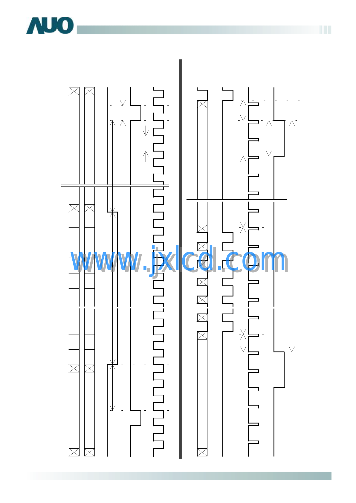
6.5 Power ON/OFF Sequence
Vin power and B/L on/off sequence is as follows. Interface signals are also shown in the chart. Signals from
any system shall be Hi-Z state or low level when Vin is off.
90%90%
90%90%
90%90%
10%
10%
Vin10%
Vin10%
Vin10%
0V
0V
0V
Signal
Signal
Signal
0V
0V
0V
10%
T2T5T6T7
T2T5T6T7
T2T5T6T7
T1
T1
T1
10%
10%
10%
T4
T4
T3
T3
T3
Lamp
Lamp
Lamp
0V
0V
0V
www.jxlcd.com
www.jxlcd.com
Symbol
T1 0.5 - 10 [ms]
T2 0.5 40 50 [ms]
T3 300 - - [ms]
T4 300 - - [ms]
T5 0.5 16 50 [ms]
T6 0.5 - 50 [ms]
T7 1000 - - [ms]
Min Typ Max
Values
T4
Unit
Ver0.1
19
Page 20
Product Specification
M230UW01 V.1
7.0 Connector & Pin Assignment
Physical interface is described as for the connector on module.
These connectors are capable of accommodating the following signals and will be following components.
7.1 TFT LCD Module
Connector Name / Designation Interface Connector / Interface card
Manufacturer JAE or compatible
Type Part Number FI-X30SSL-HF (On board Strong type)
Mating Housing Part Number
FI-X30HL-T (Locked Type)
FI-X30S-H (Unlocked Type)
7.2 Backlight Unit
-Inverter connector: JST S14B-PH-SM3 or equivalent
-Mating connector: JST PHR-14 or equivalent
Pin No. Symbol Description
1 V
2 V
3 V
4 V
5 V
6 GND
7 GND
8 GND
www.jxlcd.com
www.jxlcd.com
DDB
DDB
DDB
DDB
DDB
Power supply +24.0V
Power Ground
9 GND
10 GND
11 Open No Connection
12 V
13 V
14 Open No Connection
Ver0.1
Backlight On/Off signal
ON/OFF
Brightness adjustable voltage
BR
20
Page 21
Product Specification
M230UW01 V.1
8.0 Reliability
Reliability item and test condition
No Test Item Test Condition Note
1 Temperature Humidity Bias (THB) 50, ℃ 80%, 300hours
2
High Temperature Operation (HTO) 50, 300hours℃
3 Low Temperature Operation (LTO) 0, 300hours℃
4
High Temperature Storage (HTS) 60, 300hours℃
5
Low Temperature Storage (LTS) -20, 300hours℃
6
Thermal Shock Test (TST) -20℃/30min, 50℃/30min, 100 cycles
7
On/Off Test On/10sec, Off/10sec, 30,000 cycles
8
Shock Test (Non-Operating) 50G, 11ms, Half-sine wave (+ X, +Y, +Z)
9
Vibration Test (Non-Operating)
10 ESD (ElectroStatic Discharge)
11 Altitude Test
12 Drop Test The drop height is 60cm
1G(10~200~10 Hz P-P),
30 Minutes each Axis(X, Y, Z)
1. Contact Discharge: ± 8KV, 150pF(330Ω ) 1sec,
8 points, 25 times/ point.
2. Air Discharge: ± 15KV, 150pF(330Ω ) 1sec,
8 points, 25 times/ point.
Operation:10,000 ft
Non-Operation:30,000 ft
9.0 Safety
9.1 Sharp Edge Requirements
9.2 Materials
9.2.1 Toxicity
9.2.2 Flammability
www.jxlcd.com
www.jxlcd.com
There will be no sharp edges or comers on the display assembly that could cause injury.
There will be no carcinogenic materials used anywhere in the display module. If toxic
materials are used, they will be reviewed and approved by the responsible AUO Toxicologist.
All components including electrical components that do not meet the flammability grade
UL94-V1 in the module will complete the flammability rating exception approval process.
The printed circuit board will be made from material rated 94-V1 or better. The actual UL
flammability rating will be printed on the printed circuit board.
9.3 Capacitors
Ver0.1
If any polarized capacitors are used in the display assembly, provisions will be made to keep
them from being inserted backwards.
21
Page 22

Product Specification
M230UW01 V.1
Model No:
10.0 Other requirement
10.1 National Test Lab Requirement
The display module will satisfy all requirements for compliance to
UL 1950, First Edition U.S.A. Information Technology Equipment
CSA C22.2 No.950-M89 Canada, Information Technology Equipment
EEC 950 International, Information Technology Equipment
EN 60 950 International, Information Processing Equipment
(European Norm for IEC950)
10.2 Label
The label is on the panel as shown below:
M230UW01
V1
www.jxlcd.com
www.jxlcd.com
Ver0.1
22
Page 23

13.0 Mechanical Characteristics
www.jxlcd.com
www.jxlcd.com
Ver0.1
23
Page 24

www.jxlcd.com
www.jxlcd.com
Ver0.1
24
Page 25

www.jxlcd.com
www.jxlcd.com
Ver0.1
25
 Loading...