

Page 1
Product Specification
) Preliminary Specifications
(
( V ) Final Specifications
Module 16” FHD 16:9 Color TFT-LCD
with LED Backlight design
AU OPTRONICS CORPORATION
Model Name
Customer Date
www.jxlcd.com
www.jxlcd.com
Checked &
Approved by
B160HW02 V0 (HW Code: 1A)
Date
Approved by Date
Kuei Sheng Tseng 2010/6/30
Prepared by Date
Note: This Specification is subject to change
without notice.
Michael WJ Sun 2010/6/30
NBBU Marketing Division
AU Optronics corporation
B160HW02 V0 Document Version : 1.2
1 of 41
Page 2

Product Specification
AU OPTRONICS CORPORATION
Contents
1. Handling Precautions...............................................................5
2. General Description.................................................................6
2.1 General Specification......................................................................................................................6
2.2 Optical Characteristics....................................................................................................................7
3. Functional Block Diagram......................................................12
4. Absolute Maximum Ratings....................................................13
4.1 Absolute Ratings of TFT LCD Module..........................................................................................13
4.2 Absolute Ratings of Environment..................................................................................................13
5. Electrical Characteristics........................................................14
5.1 TFT LCD Module.........................................................................................................................14
5.2 Backlight Unit...............................................................................................................................17
6. Signal Interface Characteristic..............................................19
6.1 Pixel Format Image.......................................................................................................................19
6.2 Integration Interface Requirement.................................................................................................21
6.3 Interface Timing............................................................................................................................23
6.4 Power ON/OFF Sequence.............................................................................................................27
7. Panel Reliability Test.............................................................29
7.1 Vibration Test...............................................................................................................................29
7.2 Shock Test....................................................................................................................................29
www.jxlcd.com
7.3 Reliability Test..............................................................................................................................29
www.jxlcd.com
8. Mechanical Characteristics.....................................................30
8.1 LCM Outline Dimension...............................................................................................................30
9. Shipping and Package............................................................32
9.1 Shipping Label Format..................................................................................................................33
9.2 Carton Package.............................................................................................................................34
9.3 Shipping Package of Palletizing Sequence.....................................................................................35
10. Appendix.............................................................................36
10.1 EDID Description.......................................................................................................................36
B160HW02 V0 Document Version : 1.2
2 of 41
Page 3
Product Specification
environment: Operating Temperature :
AU OPTRONICS CORPORATION
Record of Revision
Version and Date Page
0.1 2010/09/07 All First Edition for Customer
0.2 2010/11/01 5 White Luminance 2D animation/3D :
230 cd/m
Luminance Uniformity 2D
animation/3D : 65% typ
Power Consumption : 18.8 / 24.9
Watt max (Include Logic and BLU
power)
Module thickness : 8.5mm Module thickness : 8.95mm
Weight : 632g typ 638g typ
6 Surface Treatment : Glare Surface Treatment : Anti-Glare
Revise 2.2 Optical Characteristics Please refer to revised version
11 Update absolute ratings of TFT LCD
module:
V
DD5
Update absolute ratings of
12
15,16
24,25 Update 6.5 Power ON/OFF
27,28 Update module appearance Please refer to p27~p28
www.jxlcd.com
www.jxlcd.com
0~50℃
Update power specification of IDD33,
IDD5 and delete inrush current and
VDD ripple
Update LED characteristics and
backlight input signal characteristics
Sequence
Old description New Description Remark
2
typ
: -0.3~+6.5V
DD33
: -0.3~22V
: 0~30mA
+0.3)V
2
, Vin, V
typ
LED
, I
LED
224 cd/m
50% typ
Please refer to 5.1.1 and 5.2.1
V
DD5
Vin : -0.3~(V
V
LED
I
LED
Operating Temperature : 0~50℃
Please refer to p12
Please refer to p15~p16
Please refer to p24~25
33 Update EDID description Please refer to p33~p38
1.0 2011/1/17 All Final the spec
8 none
9
13 Update current of the Input power Please refer to p13
15
21~2
3
B160HW02 V0 Document Version : 1.2
Note 2: Luminance measure point
Note 7: Definition of response time
VHPD :2.25(min); 3.6(max) VHPD :1.9(min); 2.7(max)
Timing Characteristics
Please refer to p9
Please refer to p21~p23
3 of 41
Page 4
Product Specification
27 Vibration: 10~500Hz Vibration: 5~500Hz
Shock: 220G, 2ms Shock: 210G, 3ms
30 Update pictures Please refer to p30
1.1 2011/2/17 7 Add light distribution Please refer to p7
AU OPTRONICS CORPORATION
16 Update the description of the Note1
and Note2
23 Update 3D timing Please refer to p23
27 Add the test and condition of the
High Temperature and High Humidity
Storage
1.2 2011/6/29 6 Weight : 638g typ 648g typ ± 30g
31 Update pictures and shipping label Please refer to p31
32 Update pictures Please refer to p32
www.jxlcd.com
www.jxlcd.com
Please refer to p16
Please refer to p27
B160HW02 V0 Document Version : 1.2
4 of 41
Page 5

Product Specification
1. Handling Precautions
1) Since front polarizer is easily damaged, pay attention not to scratch it.
2) Be sure to turn off power supply when inserting or disconnecting from input
connector.
3) Wipe off water drop immediately. Long contact with water may cause discoloration
or spots.
4) When the panel surface is soiled, wipe it with absorbent cotton or other soft cloth.
5) Since the panel is made of glass, it may break or crack if dropped or bumped on
hard surface.
6) Since PMOS is used in this module, take care of static electricity and insure human
earth when handling.
7) Do not open nor modify the Module Assembly.
8) Do not press the reflector sheet at the back of the module to any directions.
AU OPTRONICS CORPORATION
9) At the insertion or removal of the Signal Interface Connector, be sure not to rotate
nor tilt the Interface Connector of the TFT Module.
11)After installation of the TFT Module into an enclosure (Notebook PC Bezel, for
example), do not twist nor bend the TFT Module even momentary. At designing the
enclosure, it should be taken into consideration that no bending/twisting forces are
applied to the TFT Module from outside. Otherwise the TFT Module may be
www.jxlcd.com
damaged.
12) Small amount of materials having no flammability grade is used in the LCD module. The
LCD module should be supplied by power complied with requirements of Limited Power
Source (IEC60950 or UL1950), or be applied exemption.
13) Disconnecting power supply before handling LCD modules, it can prevent electric shock,
DO NOT TOUCH the electrode parts, cables, connectors and LED circuit part of TFT
module that a LED light bar build in as a light source of back light unit. It can prevent
electrostatic breakdown.
www.jxlcd.com
B160HW02 V0 Document Version : 1.2
5 of 41
Page 6
Product Specification
Length
-
375.0
-
Width
-
218.0
-
Thickness
- - 8.95
2. General Description
B160HW02 V0 is a Color Active Matrix Liquid Crystal Display composed of a TFT LCD
panel, a driver circuit, and LED backlight system. The screen format is intended to support
the 16:9 FHD, 1920(H) x1080(V) screen and 262k colors (RGB 6-bits data driver) with LED
backlight driving circuit. All input signals are eDP interface compatible.
B160HW02 V0 is designed for a display unit of notebook style personal computer and
industrial machine.
2.1 General Specification
The following items are characteristics summary on the table at 25 ℃ condition:
Items Unit Specifications
Screen Diagonal [mm] 406.4
Active Area [mm] 354.24X199.26
AU OPTRONICS CORPORATION
Pixels H x V 1920x3(RGB) x 1080
Pixel Pitch [mm] 0.1845X0.1845
Pixel Format R.G.B. Vertical Stripe
Display Mode Normally White
www.jxlcd.com
White Luminance 2D still picture
(ILED=20mA)
White Luminance 2D animation/3D
(ILED=27mA / 45% duty)
Luminance Uniformity 2D still picture
Luminance Uniformity 2D
animation/3D
Contrast Ratio 500 typ.
Response Time [ms] 4 Max
Nominal Input Voltage VDD [Volt] +3.3 / +5.0 typ.
Weight [Grams] 648 typ.± 30
Physical Size
Include bracket & PCBA
Electrical Interface eDP
www.jxlcd.com
[cd/m2] 345 typ.
[cd/m2]
[%] 65 typ.
[%] 50 typ.
[mm]
224 typ.
Min. Typ. Max.
Glass Thickness [mm] 0.5
Surface Treatment Anti-Glare
B160HW02 V0 Document Version : 1.2
6 of 41
Page 7

Product Specification
Storage (Non
-
Operating)
[oC]
-
20 to +60
= 20mA(rms)
= 27mA(rms),
Support Color 262K colors ( RGB 6-bit )
AU OPTRONICS CORPORATION
Temperature Range
Operating
2.2 Optical Characteristics
The optical characteristics are measured under stable conditions at 25℃ (Room Temperature) :
Item Symbol
Luminance 2D still
picture
Luminance 2D
animation/3D
Viewing Angle
Light distribution
Luminance Uniformity
2D still picture
www.jxlcd.com
Luminance Uniformity
2D animation/3D
www.jxlcd.com
[cd/m2]
[cd/m2]
θ
R
θ
L
ψ
H
ψ
L
θ=0°, ψ=0° Gray Scale
Level=L63 (White)
θ=0°, ψ=0° Gray Scale
Level=L63 (White)
Horizontal (Right)
CR = 10 (Left)
Vertical (Upper)
CR = 10 (Lower)
θ L = 1/2 Lstill
Lstill
L3D
θ=0°, ψ=0° Gray Scale
Level=L63 (White)
θ=0°, ψ=0° Gray Scale
Level=L63 (White)
[oC]
0 to +50
Conditions Min. Typ. Max. Unit Note
I
LED
LED
1, 2
1, 2
45%duty
5, 8
Vertical
Horizontal
242 345
157 224
80
80
80
80
-
-
-
-
29.5 34.5
47.0 52.0
I
-
-
degree
-
-
-
degree
degree
55 65
40 50
1, 3, 4
1, 3, 4
Contrast Ratio CR
Response Time
Red
Color /
Green
Chromaticity
Coodinates
Blue
White
NTSC (u’v’) %
2D Image sticking
300 500 -
Tr Rising
Tf Falling
TRT Rising + Falling
Rx
Ry
Gx
Gy
Bx
CIE 1931
By
Wx
Wy
Immediately after againg
5, 6
-
- - -
-
-
msec 5, 7
- - 4
0.5981 0.6481 0.6977
0.2867 0.3366 0.3847
0.2464 0.2964 0.3460
0.5922 0.6421 0.6902
0.0927 0.1427 0.1923
0.0000 0.0383 0.0864
0.2675 0.3175 0.3671
0.2680 0.3179 0.3660
5
- 100 -
There must not be image sticking in
the entire checker pattern
9
B160HW02 V0 Document Version : 1.2
7 of 41
Page 8
Product Specification
Using 13% ND
Using 13% ND
AU OPTRONICS CORPORATION
Gray(L31) is displayed for
30minutes after againg
3D Image sticking
Note 1: Turn off the white balance and measure it.
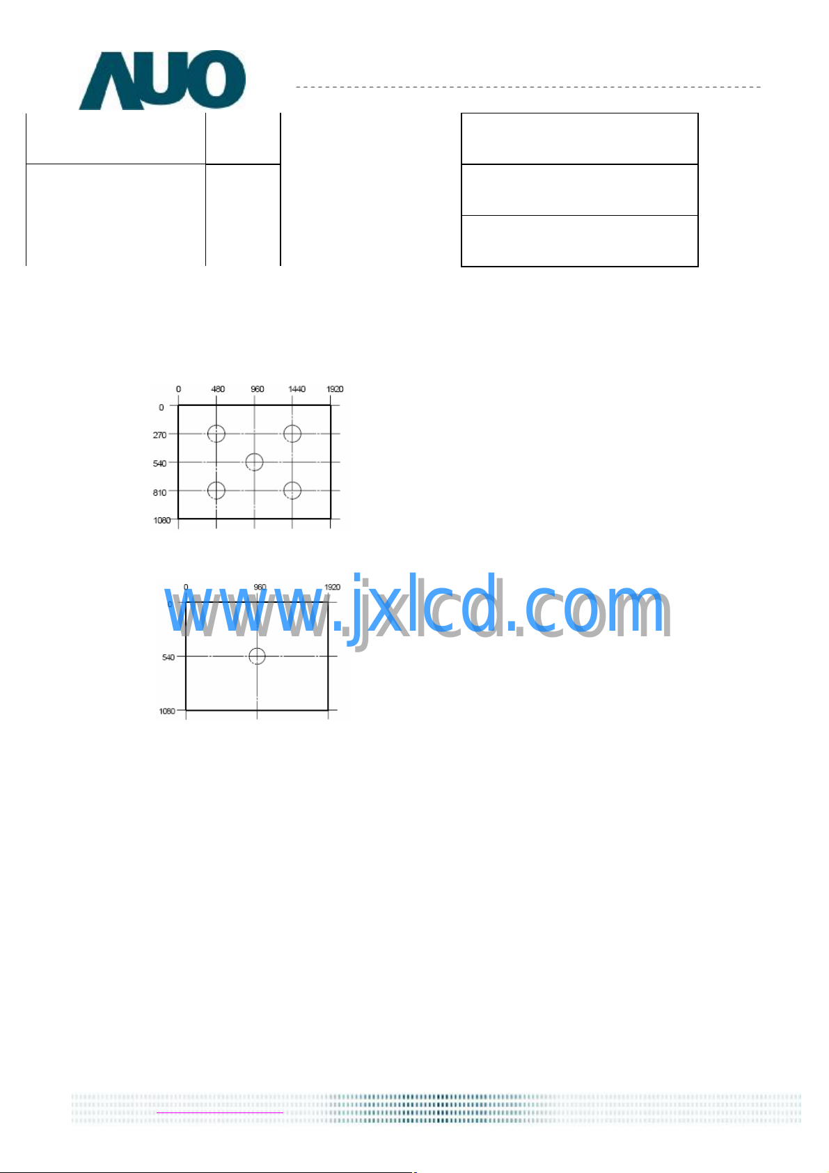
Note 2: Luminance measure point
2D still: The average value of the brightness of five points.
Immediately after againg
Gray(L31) is displayed for
30minutes after againg
No image sticking
filter
There must not be image sticking in
9
the entire checker pattern
No image sticking
filter
2D animation/ 3D: The brightness of center point
www.jxlcd.com
www.jxlcd.com
Note 3: The above test limit must be applied for initial use. Characteristics will be shifted by long period
operation, but it is not irregular phenomena. Theoretically brightness characteristics will be decreased due to
LED degradation and color shift due to optical components change.
Note 4: 9 positions position (Ref: Active area)
B160HW02 V0 Document Version : 1.2
8 of 41
Page 9
Product Specification
Field=2
°
Contrast ratio (CR)=
Brightness on the “White” state
Brightness on the “Black” state
Note 5: Measurement method
The LCD module should be stabilized at given temperature for 30 minutes to avoid abrupt temperature
change during measuring. In order to stabilize the luminance, the measurement should be executed after
AU OPTRONICS CORPORATION
lighting Backlight for 30 minutes in a stable, windless and dark room, and it should be measured in the center
of screen.
Photo detector
www.jxlcd.com
www.jxlcd.com
Note 6: Definition of contrast ratio:
Contrast ratio is calculated with the following formula.
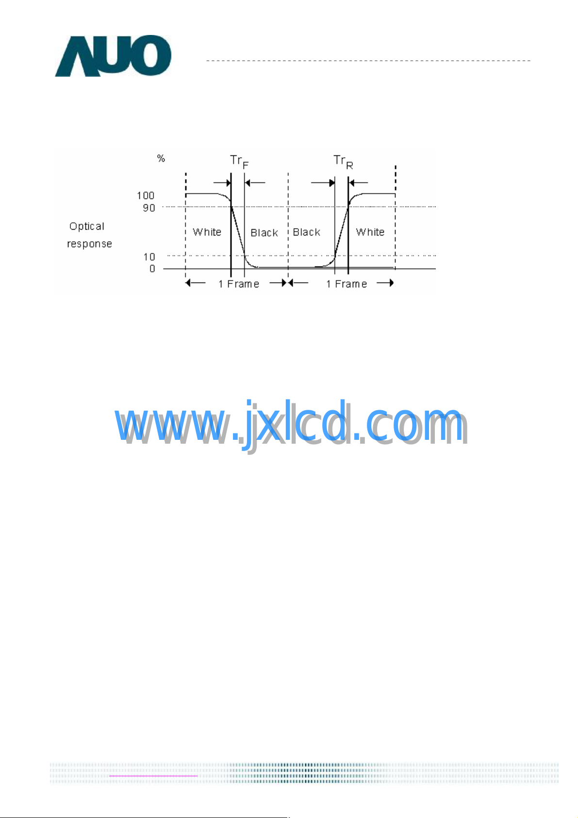
Note 7: Definition of response time: measured by Westar TRD-100A
The output signals of photo detector are measured when the input signals are changed from “Black” to
B160HW02 V0 Document Version : 1.2
9 of 41
Page 10
Product Specification
“White” (rising time, TrR), and from “White” to “Black” (falling time, TfF), respectively. The response time is
interval between the 10% and 90% of amplitudes. Refer to figure as below.
AU OPTRONICS CORPORATION
www.jxlcd.com
www.jxlcd.com
B160HW02 V0 Document Version : 1.2
10 of 41
Page 11

Product Specification
Note 8. Definition of viewing angle
Viewing angle is the measurement of contrast ratio ≧10, at the screen center, over a 180° horizontal and
180° vertical range (off-normal viewing angles). The 180° viewing angle range is broken down as follows; 90°
(θ) horizontal left and right and 90° (Φ) vertical, high (up) and low (down). The measurement direction is
typically perpendicular to the display surface with the screen rotated about its center to develop the desired
measurement viewing angle.
AU OPTRONICS CORPORATION
Note 9. (1)Image sticking in white and a black boundary part of the checkers pattern is allowed.
(2)Test pattern and method
www.jxlcd.com
www.jxlcd.com
B160HW02 V0 Document Version : 1.2
11 of 41
Page 12
Product Specification
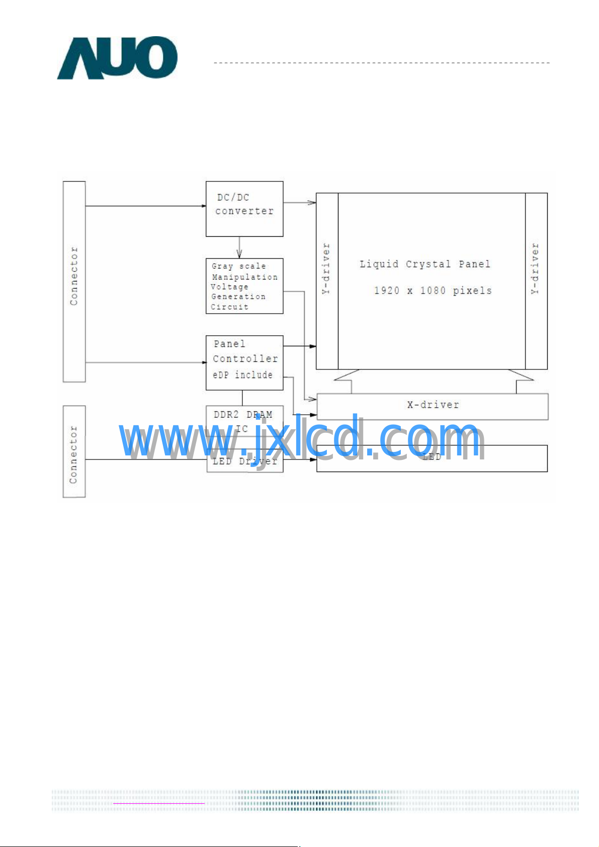
3. Functional Block Diagram
The following diagram shows the functional block of the 16 inches wide Color TFT/LCD 30 pin eDP
Module
AU OPTRONICS CORPORATION
www.jxlcd.com
www.jxlcd.com
B160HW02 V0 Document Version : 1.2
12 of 41
Page 13

Product Specification
4. Absolute Maximum Ratings
An absolute maximum rating of the module is as following:
4.1 Absolute Ratings of TFT LCD Module
Item Symbol Min Max Unit Conditions
AU OPTRONICS CORPORATION
Logic/LCD Drive Voltage V
Logic/LCD Drive Voltage V
Input Voltage of Signals VIN -0.3 V
LED Driver Supply Voltage
LED Input Current I
-0.3 +4.0 [Volt]
DD33
-0.3 +6.5 [Volt] Note 1,2
DD5
+0.3 [Volt]
DD33
V
-0.3 22 [Volt] Note 3
LED
0 30 [mA] Note 3
LED
4.2 Absolute Ratings of Environment
Item Symbol Min Max Unit Conditions
Operating Temperature TOP 0 +50 [oC] Note 4
Operation Humidity HOP 10 90 [%RH] Note 4
Storage Temperature
Storage Humidity HST
Note 1: At Ta (25℃ )
Note 2: Permanent damage to the device may occur if exceed maximum values
Note 3: LED specification refer to section 5.2
Note 4: For quality performance, please refer to AUO IIS (Incoming Inspection Standard).
www.jxlcd.com
www.jxlcd.com
TST -20 +60 [oC] Note 4
10 90
[%RH]
Note 4
B160HW02 V0 Document Version : 1.2
13 of 41
Page 14

Product Specification
5. Electrical Characteristics
5.1 TFT LCD Module
5.1.1 Power Specification
Input power specifications are as follows;
The power specification are measured under 25±5℃ and 65±20%(RH). Timing is tyical value.
AU OPTRONICS CORPORATION
Symble Parameter Min Typ
VDD33
VDD5
I
DD33
I
DD33
I
DD33
I
DD33
I
DD5
I
DD5
I
DD5
I
DD5
Note 1 : Supply voltage: VDD33=3.3V and VDD5= 5V.
www.jxlcd.com
Logic/LCD Drive Voltage
Logic/LCD Drive Voltage
3.3V 2D still picture
Color Bar
3.3V 2D still picture
checker
3.3V 2D animation/3D
Color Bar
3.3V 2D animation/3D
checker
5.0V 2D still picture
Color Bar
5.0V 2D still picture
checker
5.0V 2D animation/3D
Color Bar
5.0V 2D animation/3D
www.jxlcd.com
checker
3.0 3.3 3.6
4.5 5.0 5.5
-
-
-
-
-
-
-
-
0.46
0.47
0.63
0.66
0.65
0.90
0.52
0.88
Max Units Note
[Volt]
[Volt]
0.55
0.56
0.76
0.79
0.77
1.08
0.62
1.06
[A] Note 1
[A] Note 1
[A] Note 1
[A] Note 1
[A] Note 1
[A] Note 1
[A] Note 1
[A] Note 1
B160HW02 V0 Document Version : 1.2
14 of 41
Page 15

Product Specification
5.1.2 Signal Electrical Characteristics
Input signals shall be low or High-impedance state when VDD is off.
It is recommended to refer the specifications of VESA Display Port Standard V1.1a in
detail.
Signal electrical characteristics are as follows;
Display Port main link signal:
AU OPTRONICS CORPORATION
Fallow as VESA display port standard V1.1a at both 1.62 and 2.7Gbps link rates.
www.jxlcd.com
www.jxlcd.com
B160HW02 V0 Document Version : 1.2
15 of 41
Page 16

Display Port AUX_CH signal:
Product Specification
AU OPTRONICS CORPORATION
www.jxlcd.com
www.jxlcd.com
Fallow as VESA display port standard V1.1a.
Display Port VHPD signal:
B160HW02 V0 Document Version : 1.2
16 of 41
Page 17

5.2 Backlight Unit
5.2.1 LED characteristics
Parameter Symbol Min
B/L Power
2D still picture
Product Specification
AU OPTRONICS CORPORATION
P
Typ(Note1
- 10.5 14.4
LED2D
Max(Note2) Units
[Watt]
Condition
LED Current
20mA
B/L Power
2D animation / 3D
P
- 6.9 8.9
LED3D
B/L Power Peak
P
2D animation / 3D
Note 1: The input voltage range is between 8V and 21V, and Typ. value is a value at the condition that the input
voltage is 12 V and ambient temperature is 25 degree C.
Note 2: Max. value is a value at the condition that the input voltage is 8 V and ambient temperature is 0 degree
C.
Note 3: B/L Power 2D animation/3D is the average value of power consumption when B/L lights and B/L
non-lights in 2D animation/3D mode. B/L Power peak 2D animation/3D is the power consumption when
www.jxlcd.com
www.jxlcd.com
B/L lights in 2D animation/3D mode.
LED3D peak
- 15.4 19.8
[Watt]
[Watt]
LED Current
27mA, Duty 45%
Note3
LED Current
27mA
B160HW02 V0 Document Version : 1.2
17 of 41
Page 18

Product Specification
Connector
Connector
5.2.2 Backlight input signal characteristics
AU OPTRONICS CORPORATION
Parameter Symbol Min Typ Max Units
LED Power Supply VLED 8.0 - 21.0 [Volt]
V
2.1 3.3 3.6 [Volt]
BL/ON
LED B/L Signal Voltage
(ON/OFF)
PWM signal Voltage
PWM Input Frequency
PWM Duty Ratio
www.jxlcd.com
www.jxlcd.com
V
V
V
FPWM 20 22 24
0 - 0.5 [Volt]
BL/OFF
PWMON
PWMOFF
Duty 12 - 100
2.1 3.3 3.6
0.0 - 0.5
[Volt]
[Volt]
KHz
%
Remark
The frequency is selected
within the range from 10
to 30kHz
Input Signal Voltage
Output Signal Voltage
B160HW02 V0 Document Version : 1.2
VLR 2.1 3.3 3.6
V
EMITTER
2.1 3.3 3.6
[Volt]
[Volt]
19pin of interface
18pin of interface
18 of 41
Page 19

Product Specification
R G B R G
R G B R G B R G B R G B R G B 1
6. Signal Interface Characteristic
6.1 Pixel Format Image
Following figure shows the relationship of the input signals and LCD pixel format.
AU OPTRONICS CORPORATION
1920
1st Line
1080th Line
R G
www.jxlcd.com
www.jxlcd.com
B160HW02 V0 Document Version : 1.2
19 of 41
Page 20

Product Specification
AU OPTRONICS CORPORATION
www.jxlcd.com
www.jxlcd.com
B160HW02 V0 Document Version : 1.2
20 of 41
Page 21

Product Specification
6.2 Integration Interface Requirement
6.2.1 Connector Description
Physical interface is described as for the connector on module.
These connectors are capable of accommodating the following signals and will be following
components.
Connector Name / Designation For Signal Connector
Manufacturer I-PEX
AU OPTRONICS CORPORATION
Type / Part Number
Connector Name / Designation For LED Connector
Manufacturer J.S.T Connector
Type / Part Number
6.2.2 Pin Assignment
Signal Connector
PIN# Signal Name
1 (N.C) HPD AUX CH-Hot Plug Detect
2 AUX- AUX CH3 AUX+ AUX CH+
www.jxlcd.com
www.jxlcd.com
CABLINE-VS O.5mm Pitch 30pin, DETUM Mark(1pin Mark)
SHL connector 1.0mm pitch 14pin
20455-030E-02
SM14B-SHLK-1-TF
Description
4
5 LANE0- Main_Link06
7
8 LANE2+ Main_Link2+
9 LANE2- Main_Link210 LANE3+ Main_Link3+
11 LANE3- Main_Link312 N. C(SCL_1) N. C(GAMMA correction)
13 N. C(SDA_1) N. C(GAMMA correction)
14 N. C(GAMMA) N. C(GAMMA, EDID Write Protect)
15 N. C(SCL_2) N. C(eDP and other data correction)
16 N. C(SDA_2) N. C(eDP and other data correction)
17 N. C(WP) N. C(eDP Write Protect)
B160HW02 V0 Document Version : 1.2
LANE0+ Main_Link0+
LANE1+ Main_Link1+
LANE1- Main_Link1-
21 of 41
Page 22

Product Specification
18 EMITTER EMITTER output
19 L/R L/R ident input (Right and left identification signal)
20 N. C
21 VDD3 Logic VDD(3.3V)(DiscreateAWG#32 Use)
22 VDD3 Logic VDD(3.3V)(DiscreateAWG#32 Use)
23 VDD3 Logic VDD(3.3V)(DiscreateAWG#32 Use)
24 VDD5 Logic VDD(5.0V)(DiscreateAWG#32 Use)
25 VDD5 Logic VDD(5.0V)(DiscreateAWG#32 Use)
26 VDD5 Logic VDD(5.0V)(DiscreateAWG#32 Use)
27 GND GND(DiscreateAWG#32 Use)
28 GND GND(DiscreateAWG#32 Use)
29 GND GND(DiscreateAWG#32 Use)
30 GND GND(DiscreateAWG#32 Use)
AU OPTRONICS CORPORATION
Note 1) Please connect GND pin to ground. Don’t use it as no-connect nor connection with high impedance.
Note 2) Please connect NC to nothing. Don’t connect it to ground to other signal input.
Note 3) The signal from Pin No. 12 to No. 17 is connected with 2.5V power supply through the resistance of
10KΩ.
LED Connector
www.jxlcd.com
PIN# Signal Name
1 VDD B/L LED Driver VDD(8-21V)(DiscreteAWG#32 Use)
2 VDD B/L LED Driver VDD(8-21V)(DiscreteAWG#32 Use)
3 VDD B/L LED Driver VDD(8-21V)(DiscreteAWG#32 Use)
4 VDD B/L LED Driver VDD(8-21V)(DiscreteAWG#32 Use)
5 LED-GND
6 LED-GND
7 LED-GND
8 LED-GND
9 N.C N.C
www.jxlcd.com
LED Driver GND(DiscreteAWG#32 Use)
LED Driver GND(DiscreteAWG#32 Use)
LED Driver GND(DiscreteAWG#32 Use)
LED Driver GND(DiscreteAWG#32 Use)
Description
10 N.C N.C
11 N.C N.C
12 PWM PWM signal(Brightness control)
13 B/L EN Backlight ON/OFF
14 N.C N.C
B160HW02 V0 Document Version : 1.2
22 of 41
Page 23

Product Specification
6.3 Interface Timing
6.3.1 Timing Characteristics
www.jxlcd.com
B160HW02 V0 Document Version : 1.2
www.jxlcd.com
AU OPTRONICS CORPORATION
23 of 41
Page 24

Product Specification
www.jxlcd.com
www.jxlcd.com
AU OPTRONICS CORPORATION
B160HW02 V0 Document Version : 1.2
24 of 41
Page 25

Product Specification
www.jxlcd.com
www.jxlcd.com
AU OPTRONICS CORPORATION
a6.3.2 eDP Specification
Refer to VESA Display port Ver.1.1a.
B160HW02 V0 Document Version : 1.2
25 of 41
Page 26

6.3.3 Timing diagram
Product Specification
AU OPTRONICS CORPORATION
www.jxlcd.com
www.jxlcd.com
B160HW02 V0 Document Version : 1.2
26 of 41
Page 27

Product Specification
6.4 Power ON/OFF Sequence
Power on/off sequence is as follows. Interface signals and LED on/off sequence are also shown in
the chart.
AU OPTRONICS CORPORATION
www.jxlcd.com
www.jxlcd.com
B160HW02 V0 Document Version : 1.2
27 of 41
Page 28

Product Specification
AU OPTRONICS CORPORATION
www.jxlcd.com
www.jxlcd.com
B160HW02 V0 Document Version : 1.2
28 of 41
Page 29

Product Specification
Humidity
Humidity
7. Panel Reliability Test
7.1 Vibration Test
Test Spec:
l Test method: Non-Operation
l Acceleration: 1.5 G
l Frequency: 5 - 500Hz Random
l Sweep: 30 Minutes each Axis (X, Y, Z)
9
7.2 Shock Test
Test Spec:
l Test method: Non-Operation
l Acceleration: 210 G , Half sine wave
l Active time: 3 ms
AU OPTRONICS CORPORATION
l Pulse: X,Y,Z .one time for each side
7.3 Reliability Test
Items
High Temperature and High
Operation
High Temperature and High
Storage
Definitions of failure for judgment shall be as follows:
www.jxlcd.com
www.jxlcd.com
High Temperature Operation
Low Temperature Operation
High Temperature Storage
Low Temperature Storage
Thermal Shock Test
Required Condition Note
Ta= 45℃, 90%RH, 48h
Ta= 50℃, 90%RH, 48h
Ta= 50℃, 48h
Ta= 0℃, 48h
Ta= 65℃, 48h
Ta= -30℃, 48h
Ta=-30℃ 2.0h to 65℃ 2.0h, 12 cycles
1) Function of the module should be maintained.
2) Current consumption should be smaller than the specified value.
3) Appearance and display quality should not have distinguished degradation.
B160HW02 V0 Document Version : 1.2
4) Luminance should be larger than 50% of the minimum value specified in 2.2.
29 of 41
Page 30

30
of
41
Product Specification
B
160HW02 V0
Document Version : 1.2
8. Mechanical Characteristics
8.1 LCM Outline Dimension
8.1.1 Standard Front View
AU OPTRONICS CORPORATION
www.jxlcd.com
www.jxlcd.com
Page 31

31
of
41
B
160HW02 V0
Document Version : 1.2
8.1.2 Standard Rear View
Product Specification
AU OPTRONICS CORPORATION
www.jxlcd.com
www.jxlcd.com
Page 32

32
of
41
Product Specification
B
160HW02 V0
Document Version : 1.2
AU OPTRONICS CORPORATION
www.jxlcd.com
www.jxlcd.com
Page 33

33
of
41
Product Specification
B
160HW02 V0
Document Version : 1.2
9. Shipping and Package
9.1 Shipping Label Format
AU OPTRONICS CORPORATION
www.jxlcd.com
www.jxlcd.com
Shipping Label Position
Page 34

34
of
41
B
160HW02 V0
Document Version : 1.2
9.2 Carton Package
Product Specification
AU OPTRONICS CORPORATION
www.jxlcd.com
www.jxlcd.com
Page 35

35
of
41
Product Specification
B
160HW02 V0
Document Version : 1.2
9.3 Shipping Package of Palletizing Sequence
AU OPTRONICS CORPORATION
www.jxlcd.com
www.jxlcd.com
Page 36

36
of
41
B
160HW02 V0
Document Version : 1.2
10. Appendix
10.1 EDID Description
Product Specification
AU OPTRONICS CORPORATION
www.jxlcd.com
www.jxlcd.com
Page 37

37
of
41
Product Specification
B
160HW02 V0
Document Version : 1.2
53011
5
-0Bit…
リフレッシュレート
- 60
64
番地
:
V
-
フロントホ
゚ーチ下位
4
bit + V-Sync
.
下位
4
bit
(全6
bit
711824 71
番地
:
フラグ(
E-EDID Standard Page
18
of
32
参照
)
00011000
82
番地
:
V
-
フロントホ
゚ーチ下位
4
bit + V-Sync
.
下位
4
bit
(全6
bit
891824 89
番地
:
フラグ(
E-EDID Standard Page
18
of
32
参照
)
00011000
38 D1 209 Standard Timing 1920 209
39 C0 192 ・受像可能な代表的な全ての解像度を記入。 16:9 60Hz11000000
40 01 1 ・2Byteのコードで1つの解像度を表示。
41 01 1 ・計8種類の解像度を記述出来る。
42 01 1 ・E-Timing(35-37番地)と重複しない事。
43 01 1 ・E-Timingと S-Timing のどちらかに
44 01 1 最大解像度を記述する。
45 01 1 ・未使用部分には 01 01 を入れる。
46 01 1
47 01 1 #1:(水平解像度/8 )-31 → 16進数
48 01 1 #2: 7-6Bit… アスペクト比
49 01 1 16:10 → 0,0
50 01 1 4:3 → 0,1
51 01 1 5:4 → 1,0
52 01 1 16:9 → 1,1
AU OPTRONICS CORPORATION
54 80 128
55 70 112 54,55番地:ピクセルクロック/10000 288MHz 28800
56 80 128 56番地:水平表示期間(pixels)/下位8bit(全12bit) 1920Pixels100000001920
57 C0 192 57番地:水平ブランキング(pixels) /下位8bit(全12bit) 1216Pixels110000001216
58 74 116 58番地:H-A上位4bit + H-B上位4bit 01110100
59 38 56 59番地:垂直表示期間(lines)/下位8bit(全12bit) 1080Lines001110001080
60 90 144 60番地:垂直ブランキング(lines)/下位8bit(全12bit) 144Lines 10010000 144
61 40 64 61番地:V-A上位4bit + V-B上位4bit 01000000
62 D0 208 62番地:H-Sync. Offset(フロントポーチ)/下位8bit(全10bit) 976Pixels11010000 976
63 50 80 63番地:H-Sync.(パルス幅)/下位8bit(全10bit) 80Pixels 01010000 80
64 A6 166
65 C8 200 65番地:コメント参照 11001000
66 63 99 66番地:画面サイズ横(mm) /下位8bit(全12bit) 355mm 01100011 355
67 C8 200 66番地:画面サイズ縦(mm) /下位8bit(全12bit) 200mm 11001000 200
68 10 16 68番地:画面サイズ上位4bit + 画面サイズ縦上位4bit 00010000
69 00 0 69番地:H-Border(全8bit) 0Pixels 00000000 0
70 00 0 70番地:V-Border(全8bit) 0Lines 00000000 0
72 80 128 Detailedタイミング 1920x1080, 120(119.88)Hz, 3D
73 70 112 72,73番地:ピクセルクロック/10000 288MHz 28800
74 80 128 74番地:水平表示期間(pixels)/下位8bit(全12bit) 1920Pixels100000001920
75 B4 180 75番地:水平ブランキング(pixels)/下位8bit(全12bit) 180Pixels10110100 180
76 70 112 76番地:H-A上位4bit + H-B上位4bit 01110000
77 38 56 77番地:垂直表示期間(lines)/下位8bit(全12bit) 1080Lines001110001080
78 40 64 78番地:垂直ブランキング(lines)/下位8bit(全12bit) 64Lines 01000000 64
79 40 64 79番地:V-A上位4bit + V-B上位4bit 01000000
80 78 120 80番地:H-Sync. Offset(フロントポーチ)/下位8bit(全10bit) 120Pixels01111000 120
81 28 40 81番地:H-Sync.(パルス幅)/下位8bit(全10bit) 40Pixels 00101000 40
82 8C 140
83 04 4 83番地:コメント参照 00000100
84 63 99 84番地:画面サイズ横(mm) /下位8bit(全12bit) 355mm 01100011 355
85 C8 200 85番地:画面サイズ縦(mm) /下位8bit(全12bit) 200mm 11001000 200
86 10 16 86番地:画面サイズ上位4bit + 画面サイズ縦上位4bit 00010000
87 00 0 87番地:H-Border(全8bit) 0Pixels 00000000 0
88 00 0 88番地:V-Border(全8bit) 0Lines 00000000 0
Preferredタイミング(24番地のフラグを立てておく)1920x1080, 75Hz, 2D
42/6Lines10100110
www.jxlcd.com
www.jxlcd.com
24/12Lines10001100
Page 38

38
of
41
Product Specification
B
160HW02 V0
Document Version : 1.2
AU OPTRONICS CORPORATION
www.jxlcd.com
www.jxlcd.com
Page 39

39
of
41
Product Specification
B
160HW02 V0
Document Version : 1.2
*
番地
:
V
-
フロントホ
゚ーチ下位
4
bit + V-Sync
.
下位
4
bit
(全6
bit
1491824 *
番地
:
フラグ(
E-EDID Standard Page
18
of
32
参照
)
00011000
*
番地
:
V
-
フロントホ
゚ーチ下位
4
bit + V-Sync
.
下位
4
bit
(全6
bit
1671824 *
番地
:
フラグ(
E-EDID Standard Page
18
of
32
参照
)
00011000
190000
141 28 40 *番地:H-Sync.(パルス幅)/下位8bit(全10bit) 40Pixels 00101000 40
142 0C 12
143 4C 76 *番地:コメント参照 01001100
144 63 99 *番地:画面サイズ横(mm) /下位8bit(全12bit) 355mm 01100011 355
145 C8 200 *番地:画面サイズ縦(mm) /下位8bit(全12bit) 200mm 11001000 200
146 10 16 *番地:画面サイズ上位4bit + 画 面サイズ縦上位4bit 00010000
147 00 0 *番地:H-Border(全8bit) 0Pixels 00000000 0
148 00 0 *番地:V-Border(全8bit) 0Lines 00000000 0
150 40 64 Detailedタイミング
151 38 56 1920x1080, 60(59.94)Hz, 2D 144MHz 14400
152 80 128 *番地:水平表示期間(pixels)/下位8bit(全12bit) 1920Pixels100000001920
153 B4 180 *番地:水平ブランキング(pixels) /下位8bit(全12bit) 180Pixels10110100 180
154 70 112 *番地:H-A上位4bit + H-B上位4bit 01110000
155 38 56 *番地:垂直表示期間(lines)/下位8bit(全12bit) 1080Lines001110001080
156 40 64 *番地:垂直ブランキング(lines)/下位8bit(全12bit) 64Lines 01000000 64
157 40 64 *番地:V-A上位4bit + V-B上位4bit 01000000
158 28 40 *番地:H-Sync. Offset(フロントポーチ)/下位8bit(全10bit) 40Pixels 00101000 40
159 50 80 *番地:H-Sync.(パルス幅)/下位8bit(全10bit) 80Pixels 01010000 80
160 36 54
161 00 0 *番地:コメント参照 00000000
162 63 99 *番地:画面サイズ横(mm) /下位8bit(全12bit) 355mm 01100011 355
163 C8 200 *番地:画面サイズ縦(mm) /下位8bit(全12bit) 200mm 11001000 200
164 10 16 *番地:画面サイズ上位4bit + 画 面サイズ縦上位4bit 00010000
165 00 0 *番地:H-Border(全8bit) 0Pixels 00000000 0
166 00 0 *番地:V-Border(全8bit) 0Lines 00000000 0
AU OPTRONICS CORPORATION
48/12Lines00001100
3/6Lines 00110110
168 00 0 以 下 check sum ま で null
169 00 0
170 00 0
171 00 0
172 00 0
173 00 0
174 00 0
175 00 0
176 00 0
177 00 0
178 00 0
179 00 0
180 00 0
181 00 0
182 00 0
183 00 0
184 00 0
185 00 0
186 00 0
187 00 0
188 00 0
189 00 0
www.jxlcd.com
www.jxlcd.com
Page 40

40
of
41
B
160HW02 V0
Document Version : 1.2
240000
191 00 0
192 00 0
193 00 0
194 00 0
195 00 0
196 00 0
197 00 0
198 00 0
199 00 0
200 00 0
201 00 0
202 00 0
203 00 0
204 00 0
205 00 0
206 00 0
207 00 0
208 00 0
209 00 0
210 00 0
211 00 0
212 00 0
213 00 0
214 00 0
215 00 0
216 00 0
217 00 0
218 00 0
219 00 0
220 00 0
221 00 0
222 00 0
223 00 0
224 00 0
225 00 0
226 00 0
227 00 0
228 00 0
229 00 0
230 00 0
231 00 0
232 00 0
233 00 0
234 00 0
235 00 0
236 00 0
237 00 0
238 00 0
239 00 0
Product Specification
www.jxlcd.com
www.jxlcd.com
AU OPTRONICS CORPORATION
Page 41

41
of
41
Product Specification
B
160HW02 V0
Document Version : 1.2
AU OPTRONICS CORPORATION
www.jxlcd.com
www.jxlcd.com
 Loading...