

Page 1

AU OPTRONICS CORPORATION
) Preliminary Specifications
( V
( ) Final Specifications
Product Specification
Module
Model Name
Customer Date
www.jxlcd.com
www.jxlcd.com
Checked &
Approved by
15.4” WXGA+ Color TFT-LCD
B154PW04 V2
Date
Approved by Date
Jerry Chen 12/10/2007
Prepared by Date
Note: This Specification is subject to change without
notice.
AUO NBBU spec. Template 1.0
Wisdom Che 12/10/2007
NBBU Marketing Division /
AU Optronics corporation
1 of 36
Page 2

AU OPTRONICS CORPORATION
Product Specification
Contents
1. Handling Precautions .............................................................. 4
2. General Description ................................................................ 5
2.1 General Specification ..........................................................................................................................5
2.2 Optical Characteristics ........................................................................................................................6
3. Functional Block Diagram ....................................................... 9
4. Absolute Maximum Ratings..................................................... 9
4.1 Absolute Ratings of TFT LCD Module...............................................................................................9
4.2 Absolute Ratings of Backlight Unit.....................................................................................................9
4.3 Absolute Ratings of Environment .......................................................................................................9
5. Electrical characteristics ......................................................... 9
5.1 TFT LCD Module................................................................................................................................9
5.2 Backlight Unit .....................................................................................................................................9
6. Signal Characteristic ............................................................... 9
6.1 Pixel Format Image ...........................................................................................................................98
6.2 The input data format ........................................................................................................................99
6.3 Signal Description/Pin Assignment...................................................................................................20
6.4 Interface Timing ..................................................................................................................................9
6.5 Power ON/OFF Sequence ...............................................................................................................24
www.jxlcd.com
www.jxlcd.com
7. Connector Description............................................................. 9
7.1 TFT LCD Module................................................................................................................................9
8. Dynamic Test .......................................................................... 9
8.1 Vibration Test ....................................................................................................................................96
8.2 Shock Test Spec:..................................................................................................................................9
9. Reliability................................................................................ 9
10. Mechanical Characteristics.................................................. 98
10.1 LCM Outline Dimension.................................................................................................................98
10.2 Screw Hole Depth and Center Position...........................................................................................30
11. Shipping and Package ......................................................... 31
11.1 Shipping Label Format ....................................................................................................................31
11.2 Carton package ................................................................................................................................32
11.3 Shipping package of palletizing sequence.......................................................................................32
12. Appendix: EDID description .................................................. 9
AUO NBBU spec. Template 1.0
2 of 36
Page 3

AU OPTRONICS CORPORATION
Product Specification
Record of Revision
Version and Date Page
0.1 2007/10/26 All First Edition for Customer
0.2 2007/10/27 27 No back side drawing Add back side drawing
0.3 2007/11/29 16,
0.4 2007/12/10 17 No LED Driver Pull-up resistor Add LED Driver Pull-up resistor
www.jxlcd.com
www.jxlcd.com
No LED power sequence
30
No 15 years environmentally safety
period mark
Old description New Description Remark
Add LED power sequence
Change Shipping Label Format and
adds 15 years environmentally safety
period mark
AUO NBBU spec. Template 1.0
3 of 36
Page 4

AU OPTRONICS CORPORATION
Product Specification
1. Handling Precautions
1) Since front polarizer is easily damaged, pay attention not to scratch it.
2) Be sure to turn off power supply when inserting or disconnecting from input connector.
3) Wipe off water drop immediately. Long contact with water may cause discoloration or
spots.
4) When the panel surface is soiled, wipe it with absorbent cotton or other soft cloth.
5) Since the panel is made of glass, it may break or crack if dropped or bumped on hard
surface.
6) Since CMOS LSI is used in this module, take care of static electricity and insure human
earth when handling.
7) Do not open nor modify the Module Assembly.
8) Do not press the reflector sheet at the back of the module to any directions.
9) In case if a Module has to be put back into the packing container slot after once it was
taken out from the container, do not press the center of the LED lamp Reflector edge.
Instead, press at the far ends of the LED lamp Reflector edge softly. Otherwise the TFT
Module may be damaged.
10) At the insertion or removal of the Signal Interface Connector, be sure not to rotate nor
tilt the Interface Connector of the TFT Module.
11) After installation of the TFT Module into an enclosure (Notebook PC Bezel, for
www.jxlcd.com
example), do not twist nor bend the TFT Module even momentary. At designing the
enclosure, it should be taken into consideration that no bending/twisting forces are
applied to the TFT Module from outside. Otherwise the TFT Module may be damaged.
12) Small amount of materials having no flammability grade is used in the LCD module. The
LCD module should be supplied by power complied with requirements of Limited Power
Source (IEC60950 or UL1950), or be applied exemption.
13) The LCD module is designed so that the LED in it is supplied by Limited Current Circuit
(IEC60950 or UL1950). Do not connect the LED in Hazardous Voltage Circuit.
www.jxlcd.com
AUO NBBU spec. Template 1.0
4 of 36
Page 5
AU OPTRONICS CORPORATION
Product Specification
(Note1)
2. General Description
B154PW04 V2 is a Color Active Matrix Liquid Crystal Display composed of a TFT LCD panel, a
driver circuit, and backlight system. The screen format is intended to support the WXGA+
(1440(H) x 900(V)) screen and 262k colors (RGB 6-bits data driver) without backlight inverter. All
input signals are LVDS interface compatible.
B154PW04 V2 is designed for a display unit of notebook style personal computer and industrial
machine.
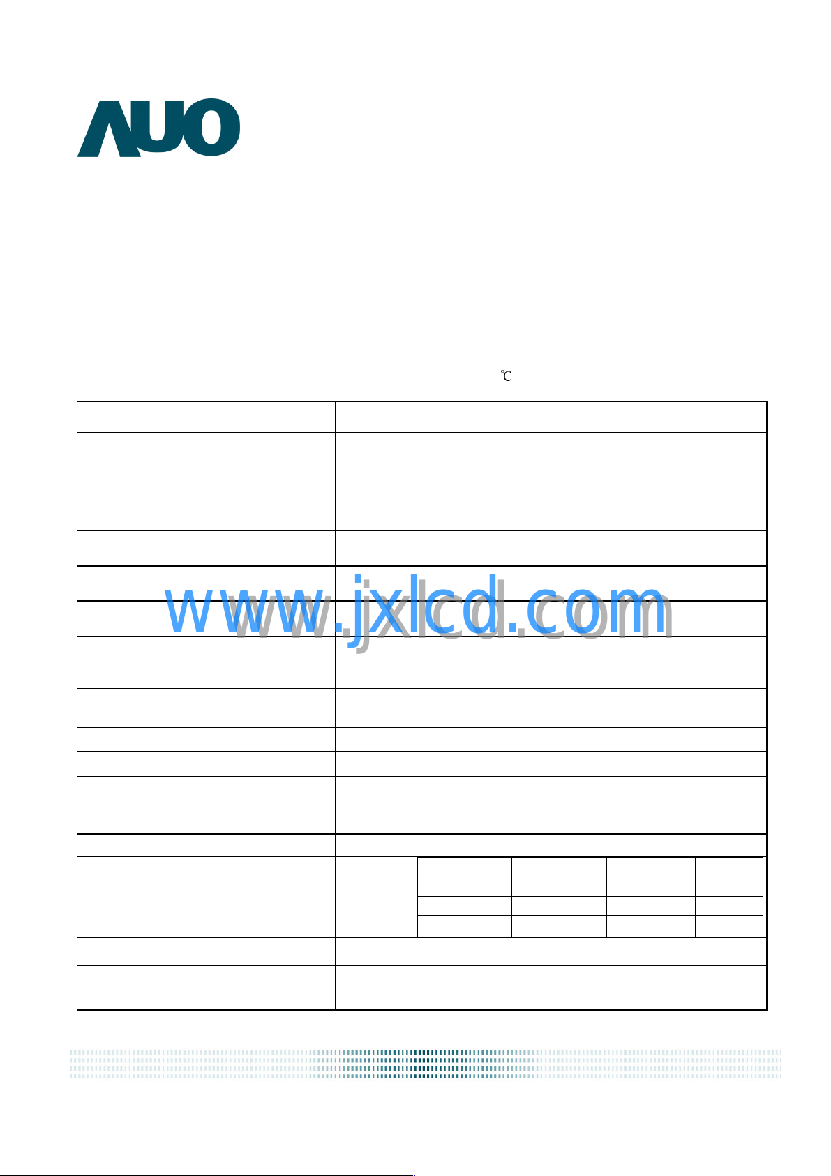
2.1 General Specification
The following items are characteristics summary on the table at 25 ℃ condition:
Items Unit Specifications
Screen Diagonal [mm] 391 (15.4W”)
Active Area [mm] 331.560 (H) X 207.225 (V)
Pixels H x V 1440x3(RGB) x 900
Pixel Pitch [mm] 0.23025X0.23025
Pixel Format R.G.B. Vertical Stripe
Display Mode Normally White
www.jxlcd.com
White Luminance (I
Note: I
Luminance Uniformity 1.25 max. (5 points)
Contrast Ratio 600 typ
Response Time [ms] 16 typ
www.jxlcd.com
LED
=19mA)
LED
is lamp current
[cd/m2] 300 typ.(5 points average)
270 min.(5 points average)
1.53 max. (13 points)
Nominal Input Voltage VDD [Volt] +3.3 typ.
Power Consumption [Watt] 5.8 max.
Weight [Grams] 460 max.
Physical Size
Electrical Interface Dual channel LVDS
Surface Treatment Glare, Hardness 3H,
AUO NBBU spec. Template 1.0
[mm]
L W T
Max 344.5 222.5 6.1
Typical 344.0 222.0 -
Min 343.5 221.5 -
5 of 36
Page 6
AU OPTRONICS CORPORATION
Product Specification
Support Color 262K colors ( RGB 6-bit )
Temperature Range
Operating
Storage (Non-Operating)
RoHS Compliance RoHS Compliance
[oC]
[oC]
0 to +50
-25 to +65
2.2 Optical Characteristics
The optical characteristics are measured under stable conditions at 25℃ (Room Temperature) :
Item Unit Conditions Min. Typ. Max. Note
White Luminance
I
LED
=19mA
Viewing Angle
Luminance
Uniformity
Luminance
Uniformity
CR: Contrast Ratio
Cross talk %
Response Time
Chromaticity of color
Coordinates
(CIE 1931)
www.jxlcd.com
www.jxlcd.com
NTSC %
[cd/m2]
[degree]
[degree]
[degree]
[degree]
[msec] Rising
[msec] Falling
[msec] Rising + Falling
5 points average
Horizontal
(Right)
CR = 10 (Left)
Vertical
(Upper)
CR = 10 (Lower)
5 Points
13 Points
500 600 -
4
Red x
Red y
Green x
Green y
Blue x
Blue y
White x
White y
CIE 1931
270 300 -
55
55
45
45
- - 1.25
- - 1.53
-
- 12 17
- 16 25
0.570 0.600 0.630
0.315 0.345 0.375
0.290 0.320 0.350
0.525 0.555 0.585
0.120 0.150 0.180
0.090 0.120 0.150
0.283 0.313 0.343
0.299 0.329 0.359
- 45 -
60
60
50
55
4
1, 4, 5.
-
-
8
-
-
1
2
6
7
8
8
2,8
AUO NBBU spec. Template 1.0
6 of 36
Page 7
AU OPTRONICS CORPORATION
Product Specification
=
Maximum Brightness of thirteen points
Minimum Brightness of thirteen points
Maximum Brightness of five
points
=
Minimum Brightness of five points
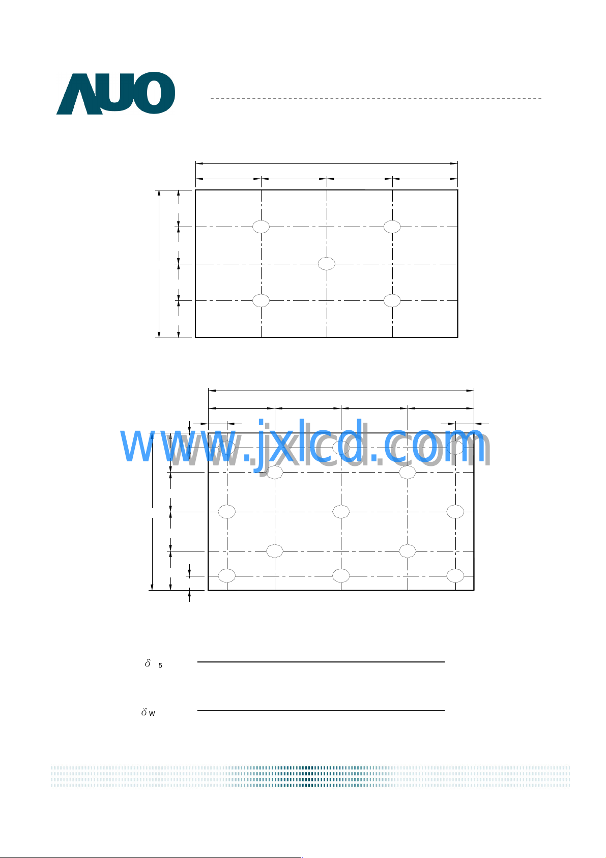
Note 1: 5 points position (Ref: Active area)
W / 4 W / 4 W /4 W / 4
H /4
W
H /4
H
H /4
H /4
Note 2: 13 points position (Ref: Active area)
W /4
1 0
1 0
www.jxlcd.com
www.jxlcd.com
H / 4
H / 4
H
1
6
1
3
4 5
W
W /4
4 5
W /4
2
7
2
W /4
1 0
3
8
H / 4
9
H / 4
1 0
1 1
1 2
Note 3: The luminance uniformity of 5 or13 points is defined by dividing the maximum luminance values by the
minimum test point luminance
δ
W5
1 0
1 3
δ
Note 4: Measurement method
AUO NBBU spec. Template 1.0
W13
7 of 36
Page 8

AU OPTRONICS CORPORATION
Product Specification
Field=2
°
Contrast ratio (CR)=
Brightness on the “White” state
Brightness on the “Black” state
The LCD module should be stabilized at given temperature for 30 minutes to avoid abrupt temperature change
during measuring. In order to stabilize the luminance, the measurement should be executed after lighting Backlight
for 30 minutes in a stable, windless and dark room.
Photo detector
Note 5: Definition of Average Luminance of White (YL):
Measure the luminance of gray level 63 at 5 points,Y
L (x) is corresponding to the luminance of the point X at Figure in Note (1).
Note 6: Definition of contrast ratio:
Note 7: Definition of Cross Talk (CT)
www.jxlcd.com
www.jxlcd.com
= [L (1)+ L (2)+ L (3)+ L (4)+ L (5)] / 5
L
Contrast ratio is calculated with the following formula.
CT = | YB – YA | / YA × 100 (%)
Where
YA = Luminance of measured location without gray level 0 pattern (cd/m2)
AUO NBBU spec. Template 1.0
8 of 36
Page 9

AU OPTRONICS CORPORATION
Product Specification
YB = Luminance of measured location with gray level 0 pattern (cd/m2)
Note 8: Definition of response time:
The output signals of BM-7 or equivalent are measured when the input signals are changed from “Black” to
“White” (falling time) and from “White” to “Black” (rising time), respectively. The response time interval between the
10% and 90% of amplitudes. Refer to figure as below.
"Black"
100%
S
i
90%
g
n
a
l
(
R
e
l
www.jxlcd.com
a
t
i
v
e
v
a
l
u
e
)
www.jxlcd.com
10%
0%
Tr
Tf
"White""White"
AUO NBBU spec. Template 1.0
9 of 36
Page 10
AU OPTRONICS CORPORATION
Product Specification
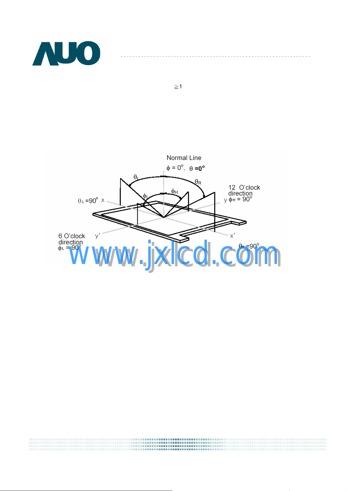
Note 8. Definition of viewing angle
Viewing angle is the measurement of contrast ratio ≧10, at the screen center, over a 180° horizontal and
180° vertical range (off-normal viewing angles). The 180° viewing angle range is broken down as follows; 90° (θ)
horizontal left and right and 90° (Φ) vertical, high (up) and low (down). The measurement direction is typically
perpendicular to the display surface with the screen rotated about its center to develop the desired measurement
viewing angle.
www.jxlcd.com
www.jxlcd.com
AUO NBBU spec. Template 1.0
10 of 36
Page 11

AU OPTRONICS CORPORATION
Product Specification
Odd
xIN0
LCD Connec to r(
50
pin)
3. Functional Block Diagram
The following diagram shows the functional block of the 15.4 inches wide Color TFT/LCD Module:
(8 pa irs LVDS )
OddxIN 1
OddxIN 2
OddxC LK IN
Even xIN0
Even xIN1
Even xIN2
Even xCLKIN
LC D DRIV E
BOARD
LC D
Controller
TFT ARRAY/CELL
1440(R /G/B) x 3 x 900
Backlight Unit
LE D
Po wer
Co ntrol Signal
VDD
GND
JAE FI-VHP50S-A-HF11
www.jxlcd.com
Mating Ho using JAE FI-VH P50C-A
www.jxlcd.com
DC-D C
Conver ter
Ref circ uit
X-Driver
Y-Driver
AUO NBBU spec. Template 1.0
11 of 36
Page 12

AU OPTRONICS CORPORATION
Product Specification
4. Absolute Maximum Ratings
An absolute maximum rating of the module is as following:
4.1 Absolute Ratings of TFT LCD Module
Item Symbol Min Max Unit Conditions
Logic/LCD Drive Voltage
Vin -0.3 +4.0 [Volt] Note 1,2
4.2 Absolute Ratings of Backlight Unit
Item Symbol Min Max Unit Conditions
LED Current ILED - 20 [mA] rms Note 1,2
4.3 Absolute Ratings of Environment
Item Symbol Min Max Unit Conditions
Operating Temperature
Operation Humidity HOP 5 95 [%RH] Note 3
Storage Temperature
Storage Humidity HST
TOP 0 +50 [oC] Note 3
TST -20 +60 [oC] Note 3
5 95
[%RH]
Note 3
Note 1: At Ta (25℃ )
Note 2: Permanent damage to the device may occur if exceed maximum values
Note 3: For quality performance, please refer to AUO IIS (Incoming Inspection Standard).
www.jxlcd.com
www.jxlcd.com
Twb=39°C
Operating Range
AUO NBBU spec. Template 1.0
Storage Range
12 of 36
Page 13

AU OPTRONICS CORPORATION
Product Specification
-
90%
10%
5. Electrical characteristics
5.1 TFT LCD Module
5.1.1 Power Specification
Input power specifications are as follows;
Symble Parameter Min Typ Max Units
VDD Logic/LCD Drive
PDD VDD Power
IDD IDD Current
I
Rush
Inrush Current
VDDrp Allowable
3.0 3.3 3.6 [Volt]
- 2 [Watt] Note 1/2
- 380
- -
- -
562
2000 [mA]
100 [mV]
Logic/LCD Drive
Ripple Voltage
Note 1 : Maximum Measurement Condition:Black Pattern
Note 2:Typical Measurement Condition: Mosaic Pattern
Note 3:Measure Condition
+5.0V
www.jxlcd.com
www.jxlcd.com
(High to Low)
Control
Signal
SW1
SW MAG-SPST
1 2
+12.0V
R1
47K
R2
1K
VR1
47K
D6
D5
D2 S
D1
G
C3
0.01uF/25V
Q3
AO6402
D2SD1D5
G
D6
Q3
AO6402
F1
[mA]
p-p
Note 1/2
Note 3
(LCD Module Input)
C1
1uF/16V
Note
VCC
AUO NBBU spec. Template 1.0
0V
C2
1uF/25V
0.5ms
Vin rising time
3.3V
13 of 36
Page 14

AU OPTRONICS CORPORATION
Product Specification
VSS
5.1.2 Signal Electrical Characteristics
Input signals shall be low or High-impedance state when VDD is off.
It is recommended to refer the specifications of THC63LVDF84A (Thine Electronics Inc.) in
detail.
Signal electrical characteristics are as follows;
Parameter
Vth
Vtl
Vcm
Note: LVDS Signal Waveform
V
t
Differential Input High
Threshold (Vcm=+1.2V)
Differential Input Low
Threshold (Vcm=+1.2V)
Differential Input
Common Mode Voltage
www.jxlcd.com
www.jxlcd.com
Condition Min Max Unit
Vcm
-
-100
1.1
100
-
1.45
[mV]
[mV]
[V]
AUO NBBU spec. Template 1.0
14 of 36
Page 15

AU OPTRONICS CORPORATION
Product Specification
5.2 Backlight Unit
The BLU system is an edge type light source with LED (Light Emitting Diode) light bar
Item Symbol Min Typ Max Units Condition
Fixed input current ILt 20 [mA] rms
Light bar Voltage
Light bar Power
Light bar PIN assignment:
www.jxlcd.com
www.jxlcd.com
PIN NO. Pin assignment Function
VL 32. 34
PL 3.7 3.88
[Volt] rms
Wt
1 VOUT LED Anode (Positive)
2 VOUT LED Anode (Positive)
3 VOUT LED Anode (Positive)
4 NC NC
5 FB6 LED Cathode (Negative)
6 FB5 LED Cathode (Negative)
7 FB4 LED Cathode (Negative)
8 FB3 LED Cathode (Negative)
9 FB2 LED Cathode (Negative)
10 FB1 LED Cathode (Negative)
AUO NBBU spec. Template 1.0
15 of 36
Page 16

AU OPTRONICS CORPORATION
LED Power Sequence
Product Specification
Valus
Symbol
T1 10 --- --- ms
T2 100 --- --- ms
www.jxlcd.com
www.jxlcd.com
T3 10 --- --- ms
Note: The duty of LED dimming signal should be more than 20% in T2..
Min Typ Max
Unit
AUO NBBU spec. Template 1.0
16 of 36
Page 17

AU OPTRONICS CORPORATION
Product Specification
LED Driver SMBUS Pull-up resistor
www.jxlcd.com
www.jxlcd.com
SMBUS Pull-up Circuitry
Setting value for Pull-up resistor Rp
−≥≥− VDDRpVDD
Suggestion: IF VDD=3.3V, Rp=10K ohm; IF VDD=5V, Rp=15K ohm
Note: Rp is the equivalent resistor for SMBUS Pull-up Circuitry
66 −−
)10*350/()4.0()10*100/()4.0(
AUO NBBU spec. Template 1.0
17 of 36
Page 18

Product Specification
AUO
6. Signal Characteristic
6.1 Pixel Format Image
Following figure shows the relationship of the input signals and LCD pixel format.
AU OPTRONICS CORPORATION
www.jxlcd.com
www.jxlcd.com
NBBU spec. Template 1.0
18 of 36
Page 19

Product Specification
AUO
6.2 The input data format
AU OPTRONICS CORPORATION
Signal Name
www.jxlcd.com
VEEDID (3.3V) +3.3V EDID Power
CLK EEDID EDID Clock Input
DATA EEDID EDID Data Input
ORXIN0-, ORXIN0+
ORXIN1-, ORXIN1+
ORXIN2-, ORXIN2+
ORXCLKIN-, ORXCLKIN+ Odd LVDS differential clock input
ERXIN0-, ERXIN0+
ERXIN1-, ERXIN1+
ERXIN2-, ERXIN2+
ERXCLKIN-, ERXCLKIN+
VDD
VSS
Note: Output signals from any system shall be low or High-impedance state when VDD is off.
www.jxlcd.com
Odd LVDS differential data input(ORed0-ORed5, OGreen0)
Odd LVDS differential data input(OGreen1-OGreen5, OBlue0-OBlue1)
Odd LVDS differential data input(OBlue2-OBlue5, Hsync, Vsync, DE)
Even LVDS differential data input(ERed0-ERed5, EGreen0)
Even LVDS differential data input(EGreen1-EGreen5, EBlue0-EBlue1)
Even LVDS differential data input(EBlue2-EBlue5)
Even LVDS differential clock input
+3.3V Power Supply
Ground
Description
NBBU spec. Template 1.0
19 of 36
Page 20

Product Specification
AUO
6.3 Signal Description/Pin Assignment
LVDS is a differential signal technology for LCD interface and high speed data transfer device.
PIN# Signal Name Description
1 Test Loop (only to pin 30) Diag. pin for test
2 VEEDID (3.3v) DDC 3.3Vpower
3 VSS Ground
4 CLK EEDID DDC Clock
5 DATA EEDID DDC Data
6 VSS Ground
7 Odd_Rin0- Odd channel Differential Data Input
8 Odd_Rin0+ Odd channel Differential Data Input
9 VSS Ground
10 Odd_Rin1- Odd channel Differential Data Input
AU OPTRONICS CORPORATION
11 Odd_Rin1+ Odd channel Differential Data Input
12 VSS Ground
13 Odd_Rin2- Odd channel Differential Data Input
14 Odd_Rin2+ Odd channel Differential Data Input
15 VSS Ground
16 Odd_ClkIN- Odd channel Differential Clock Input
17 Odd_ClkIN+ Odd channel Differential Clock Input
18 VSS Ground
19 Even_Rin0- Even channel Differential Data Input
20 Even_Rin0+ Even channel Differential Data Input
21 VSS Ground
22 Even_Rin1- Even channel Differential Data Input
23 Even_Rin1+ Even channel Differential Data Input
24 VSS Ground
25 Even_Rin2- Even channel Differential Data Input
26 Even_Rin2+ Even channel Differential Data Input
www.jxlcd.com
www.jxlcd.com
27 VSS Ground
28 Even_ClkIN- Even channel Differential Clock Input
29 Even_ClkIN+ Even channel Differential Clock Input
30 Test Loop (only to pin 1) Diag. pin for test
31 Test Loop (only to pin 50) Diag. pin for test
32 VDD Power Supply (+3.3V)
33 VDD Power Supply (+3.3V)
NBBU spec. Template 1.0
20 of 36
Page 21

Product Specification
AUO
34 TEST (BIST_EN) BIST Function
35 +5V_ALW Power Supply (+5V)
36 VSS Ground
37 VSS Ground
38 PWM_BL Systwm side PWM input signal for brightness control
39 VBL- LED Power Ground
40 VBL- LED Power Ground
41 VBL- LED Power Ground
42 VBL- LED Power Ground
43 NC No Connection
44 VBL+ Backlight Input Voltage
45 VBL+ Backlight Input Voltage
46 VBL+ Backlight Input Voltage
AU OPTRONICS CORPORATION
47 VBL+ Backlight Input Voltage
48 SMB_DATA SMBus interface for sending brightness information
49 SMB_CLK SMBus interface for sending brightness information
50 Test Loop (only to pin 31) Diag. pin for test
Note1: Start from right side
www.jxlcd.com
www.jxlcd.com
NBBU spec. Template 1.0
21 of 36
Page 22

Product Specification
AUO
6.4 Interface Timing
6.4.1 Timing Characteristics
Basically, interface timings should match the 1440x900 /60Hz manufacturing guide line timing.
Parameter Symbol Min. Typ. Max. Unit
Frame Rate - 50 60 - Hz
AU OPTRONICS CORPORATION
Clock frequency 1/ T
Vertical
Section
Horizontal
Section
Note : DE mode only
www.jxlcd.com
www.jxlcd.com
Period TV 904 912 2048
Active TVD 900 900 900
Blanking TVB 4 12 -
Period TH 760 880 1024
Active THD 720 720 720
Blanking THB 40 160 -
- 48.2 60.2 MHz
Clock
T
T
Clock
Line
NBBU spec. Template 1.0
22 of 36
Page 23

AUO
6.4.2 Timing diagram
Product Specification
AU OPTRONICS CORPORATION
www.jxlcd.com
www.jxlcd.com
NBBU spec. Template 1.0
23 of 36
Page 24

Product Specification
AUO
T3 T2
T1
T7
6.5 Power ON/OFF Sequence
VDD power and lamp on/off sequence is as follows. Interface signals are also shown in the chart.
Signals from any system shall be Hi-Z state or low level when VDD is off.
Power Supply VDD
Backlight On
www.jxlcd.com
www.jxlcd.com
Power Sequence Timing
Parameter
AU OPTRONICS CORPORATION
90%
10%
T5
Value
Min.
T1
T2
T3
T4
T5
T6
0.5
5
0.5
400
200
200
Typ.
-
-
-
-
-
-
VALID
DATA
Max.
10
50
50
-
-
-
90%
10%
T4
T6
Units
(ms)
(ms)
(ms)
(ms)
(ms)
(ms)
T7
NBBU spec. Template 1.0
0
-
10
(ms)
24 of 36
Page 25

Product Specification
AUO
7. Connector Description
Physical interface is described as for the connector on module.
These connectors are capable of accommodating the following signals and will be following
components.
7.1 TFT LCD Module
Connector Name / Designation For Signal Connector
Manufacturer JAE or compatible
AU OPTRONICS CORPORATION
Type / Part Number
Mating Housing/Part Number
www.jxlcd.com
www.jxlcd.com
JAE FI-VHP50S-A-HF11
JAE FI-VHP50C-A
or compatible
or compatible
NBBU spec. Template 1.0
25 of 36
Page 26

Product Specification
AUO
8. Dynamic Test
8.1 Vibration Test
Test condition:
Acceleration: 1.5 G
Frequency: 10 - 500Hz Random
Sweep: 30 Minutes each Axis (X, Y, Z)
8.2 Shock Test Spec:
Test condition:
Acceleration: 220 G , Half sine wave
Active time: 2 ms
Pulse: +/-X,+/-Y,+/-Z , one time for each side
AU OPTRONICS CORPORATION
Remark:
1. Ambient condition is
2.
Non-packaged and Non-operation
www.jxlcd.com
www.jxlcd.com
25 + 5℃, Relative humidity : 40% ~ 70%
NBBU spec. Template 1.0
26 of 36
Page 27

AUO
9. Reliability
Items
Product Specification
AU OPTRONICS CORPORATION
Required Condition Note
Temperature
Humidity Bias
High Temperature
Operation
Low Temperature
Operation
High Temperature
Storage
Low Temperature
Storage
Thermal Shock
Test
ESD
www.jxlcd.com
www.jxlcd.com
Ta= 40℃℃℃℃, 95%RH, 300h
Ta= 50℃℃℃℃, Dry, 300h
Ta= 0℃℃℃℃, 300h
Ta= 65℃℃℃℃, 35%RH, 300h
Ta= -25℃℃℃℃, 50%RH, 300h
Ta=-40℃℃℃℃to 65℃℃℃℃, Duration at 30 min, 100 cycles
Contact : ±8 KV
Air : ±15 KV
Note 1
Note1: According to EN 61000-4-2 , ESD class B: Some performance degradation allowed. No data lost
. Self-recoverable. No hardware failures.
Remark: MTBF (Excluding the LED): 30,000 hours with a confidence level 90%
NBBU spec. Template 1.0
27 of 36
Page 28

Product Specification
AUO
10. Mechanical Characteristics
10.1 LCM Outline Dimension
AU OPTRONICS CORPORATION
www.jxlcd.com
www.jxlcd.com
NBBU spec. Template 1.0
28 of 36
Page 29

Product Specification
AUO
AU OPTRONICS CORPORATION
www.jxlcd.com
www.jxlcd.com
NBBU spec. Template 1.0
29 of 36
Page 30

Product Specification
AUO
10.2 Screw Hole Depth and Center Position
Screw hole minimum depth, from side surface = 2.3 mm (Ref. drawing)
Screw hole center location, from front surface = 3.7 ± 0.2mm (Ref. drawing)
Screw Torque: Maximum 2.5 kgf-cm
AU OPTRONICS CORPORATION
www.jxlcd.com
www.jxlcd.com
NBBU spec. Template 1.0
30 of 36
Page 31

AUO
RoHS
11. Shipping and Package
Product Specification
AU OPTRONICS CORPORATION
11.1 Shipping Label Format
TW-0HW663-72090-XXX-XXXX
Manufactured 07/52
Model No: B154PW04
AU Optronics
MADE IN TAIWAN (M01)
V.3
C US
E204356
Pb
H/W: 0A F/W:1
REV A00
www.jxlcd.com
www.jxlcd.com
NBBU spec. Template 1.0
31 of 36
Page 32

Product Specification
AUO
11.2 Carton package
The outside dimension of carton is 455 (L)mm x 380 (W)mm x 355 (H)mm
www.jxlcd.com
www.jxlcd.com
AU OPTRONICS CORPORATION
11.3 Shipping package of palletizing sequence
NBBU spec. Template 1.0
32 of 36
Page 33

Product Specification
AUO
Value
(DEC)
12. Appendix: EDID description
Byte Value
(hex)
0 Header 00 00000000
1 Header FF 11111111
2 Header FF 11111111
3 Header FF 11111111
4 Header FF 11111111
5 Header FF 11111111
6 Header FF 11111111
7 Header 00 00000000
8 EISA manufacture code = 3 Character ID 06 00000110
9 EISA manufacture code (Compressed ASCII) AF 10101111
0A Panel Supplier Reserved – Product Code 77 01110111
0B Panel Supplier Reserved – Product Code 43 01000011
0C LCD module Serial No - Preferred but Optional (“0” if not used) 00 00000000
0D LCD module Serial No - Preferred but Optional (“0” if not used) 00 00000000
0E LCD module Serial No - Preferred but Optional (“0” if not used) 00 00000000
0F LCD module Serial No - Preferred but Optional (“0” if not used) 00 00000000
10 Week of manufacture 01 00000001
11 Year of manufacture 11 00010001
12 EDID structure version # = 1 01 00000001
www.jxlcd.com
13 EDID revision # = 3 03 00000011
14 Video I/P definition = Digital I/P (80h) 90 10010000
15 Max H image size = (Rounded to cm) 21 00100001
16 Max V image size = (Rounded to cm) 15 00010101
17
18 Feature support ( no DPMS, Active off, RGB, timing BLK 1) 0A 00001010
19 Red/Green Low bit (RxRy/GxGy) 90 10010000
1A Blue/White Low bit (BxBy/WxWy) B5 10110101
1B Red X Rx = 0.6 99 10011001
1C Red Y Ry = 0.345 58 01011000
1D Green X Gx = 0.32 52 01010010
1E Green Y Gy = 0.555 8E 10001110
1F Blue X Bx = 0.15 26 00100110
20 Blue Y By = 0.12 1E 00011110
21 White X Wx = 0.313 50 01010000
22 White Y Wy = 0.329 54 01010100
23 Established timings 1 (00h if not used) 00 00000000
24 Established timings 2 (00h if not used) 00 00000000
25 Manufacturer’s timings (00h if not used) 00 00000000
26 Standard timing ID1 (01h if not used) 01 00000001
27 Standard timing ID1 (01h if not used) 01 00000001
28 Standard timing ID2 (01h if not used) 01 00000001
www.jxlcd.com
Display gamma = (gamma ×100)-100 = Example: ( 2.2×100 ) –
100 = 120 78 01111000
AU OPTRONICS CORPORATION
Field Name and Comments
(hex) (binary)
Value
NBBU spec. Template 1.0
33 of 36
Page 34

Product Specification
AUO
29 Standard timing ID2 (01h if not used) 01 00000001
2A Standard timing ID3 (01h if not used) 01 00000001
2B Standard timing ID3 (01h if not used) 01 00000001
2C Standard timing ID4 (01h if not used) 01 00000001
2D Standard timing ID4 (01h if not used) 01 00000001
2E Standard timing ID5 (01h if not used) 01 00000001
2F Standard timing ID5 (01h if not used) 01 00000001
30 Standard timing ID6 (01h if not used) 01 00000001
31 Standard timing ID6 (01h if not used) 01 00000001
32 Standard timing ID7 (01h if not used) 01 00000001
33 Standard timing ID7 (01h if not used) 01 00000001
34 Standard timing ID8 (01h if not used) 01 00000001
35 Standard timing ID8 (01h if not used) 01 00000001
36 Pixel Clock/10,000 = 96310000 /10000 (LSB)
37 Pixel Clock/10,000 = 96310000 /10000 (MSB)
Horizontal Active = 1440 pixels
38
39 Horizontal Blanking (Thbp) = 320 pixels (lower 8 bits)
3A Horizontal Active/Horizontal blanking (Thbp) (upper4:4 bits) 51 01010001
3B Vertical Active = 900 lines 84 10000100
3C
3D
3E Horizontal Sync, Offset (Thfp) = 64 pixels 40 01000000
3F Horizontal Sync, Pulse Width = 32 pixels 20 00100000
40 Vertical Sync, Offset (Tvfp) = 3 lines Sync Width = 3 lines 33 00110011
41 Horizontal Vertical Sync Offset/Width upper 2 bits 00 00000000
42 Horizontal Image Size = 331.2 mm 4B 01001011
43 Vertical image Size = 207 mm CF 11001111
44 Horizontal Image Size / Vertical image size 10 00010000
45 Horizontal Border = 0 (Zero for Notebook LCD) 00 00000000
46 Vertical Border = 0 (Zero for Notebook LCD) 00 00000000
(lower 8 bits) A0 10100000
Vertical Blanking (Tvbp) = 12 lines (DE Blanking typ. for DE only
panels) 0C 00001100
Vertical Active : Vertical Blanking (Tvbp) (upper4:4
bits) 30 00110000
www.jxlcd.com
www.jxlcd.com
AU OPTRONICS CORPORATION
9F
25
40 01000000
10011111
00100101
if display uses standard blanking (HSyncPolarity = POS,
47
48 Pixel Clock/10,000 = 96310000 /10000 (LSB)
49 Pixel Clock/10,000 = 96310000 /10000 (MSB)
4A
4B Horizontal Blanking (Thbp) = 320 pixels (lower 8 bits)
4C Horizontal Active/Horizontal blanking (Thbp) (upper4:4 bits) 51 01010001
4D Vertical Active = 900 lines 84 10000100
4E
4F
50 Horizontal Sync, Offset (Thfp) = 64 pixels 40 01000000
51 Horizontal Sync, Pulse Width = 32 pixels 20 00100000
52 Vertical Sync, Offset (Tvfp) = 3 lines Sync Width = 3 lines 33 00110011
NBBU spec. Template 1.0
VSyncPolarity = NEG) , for DVD compliance. 1A 00011010
9F
25
Horizontal Active = 1440 pixels
(lower 8 bits) A0 10100000
40 01000000
Vertical Blanking (Tvbp) = 12 lines (DE Blanking typ. for DE only
panels) 0C 00001100
Vertical Active : Vertical Blanking (Tvbp) (upper4:4
bits) 30 00110000
10011111
00100101
34 of 36
Page 35

Product Specification
AUO
53 Horizontal Vertical Sync Offset/Width upper 2 bits 00 00000000
54 Horizontal Image Size = 331.2 mm 4B 01001011
55 Vertical image Size = 207 mm CF 11001111
56 Horizontal Image Size / Vertical image size 10 00010000
57 Horizontal Border = 0 (Zero for Notebook LCD) 00 00000000
58 Vertical Border = 0 (Zero for Notebook LCD) 00 00000000
if display uses standard blanking (HSyncPolarity = POS,
59
5A Flag 00 00000000
5B Flag 00 00000000
5C Flag 00 00000000
5D Dummy Descriptor FE 11111110
5E Flag 00 00000000
VSyncPolarity = NEG) , for DVD compliance. 1A 00011010
AU OPTRONICS CORPORATION
5F Dell P/N 1st Character
60 Dell P/N 2nd Character
61 Dell P/N 3rd Character
62 Dell P/N 4th Character
63 Dell P/N 5th Character
64 EEDID Revision = X10 0A 00001010
65 Manufacturer P/N 42 01000010
66 Manufacturer P/N 31 00110001
67 Manufacturer P/N 35 00110101
68 Manufacturer P/N 34 00110100
www.jxlcd.com
69 Manufacturer P/N 50 01010000
6A Manufacturer P/N 57 01010111
6B
6C Flag 00 00000000
6D Flag 00 00000000
6E Flag 00 00000000
6F Data Type Tag: 00 00000000
70 Flag 00 00000000
71 SMBUS Value = XX nits 26 00100110
72 SMBUS Value = XX nits 35 00110101
73 SMBUS Value = XX nits 41 01000001
74 SMBUS Value = XX nits 4A 01001010
75 SMBUS Value = XX nits 67 01100111
76 SMBUS Value = XXX nits 89 10001001
77 SMBUS Value = XXX nits B6 10110110
78 SMBUS Value = max nits (Typically = 00h, XXX nits) FF 11111111
www.jxlcd.com
Manufacturer P/N (If <13 char, then terminate with ASCII code 0Ah,
set remaining char = 20h) 34 00110100
48
57
36
36
33
01001000
01010111
00110110
00110110
00110011
Bit[1:0] 00: reserved, 01: single LVDS, 10: dual LVDS, 11: reserved
Bit[2] 0: No RTC support, 1: RTC support
79
7A
NBBU spec. Template 1.0
Bit[7:3] Reserved
Bit[0] 0: No BIST support, 1: BIST support
Bit[7:1] Reserved
02 00000010
01 00000001
35 of 36
Page 36

Product Specification
AUO
(If <13 char, then terminate with ASCII code 0Ah, set remaining char
(If <13 char, then terminate with ASCII code 0Ah, set remaining char
(If <13 char, then terminate with ASCII code 0Ah, set remaining char
AU OPTRONICS CORPORATION
7B
7C
7D
7E
7F
= 20h) 0A 00001010
= 20h) 20 00100000
= 20h) 20 00100000
Extension flag (# of optional 128 EDID extension blocks to follow,
Typ = 0) 00 00000000
Checksum (The 1-byte sum of all 128 bytes in this EDID block
shall = 0)
3E
00111110
www.jxlcd.com
www.jxlcd.com
NBBU spec. Template 1.0
36 of 36
 Loading...