

Page 1

Document Version: 2
Date: 2005/6/7
Product Functional Specification
14.1 inch XGA Color TFT LCD Module
Model Name : B141XG09 V2
www.jxlcd.com
www.jxlcd.com
( ) Preliminary Specification
(C) Copyright AU Optronics
Dec., 2002 All Rights Reserved. B141XG09 V2
No Reproduction and Redistribution Allowed.
1/26
(u) Final Specification
PDF created with FinePrint pdfFactory trial version www.pdffactory.com
Page 2

Contents
1.0 Handling Precautions...........................................................................................................4
2.0 General Description ............................................................................................................. 5
2.1 Display Characteristics.................................................................................................... 5
2.2 Functional Block Diagram ............................................................................................... 6
3.0 Absolute Maximum Ratings ................................................................................................7
4.0 Optical Characteristics ........................................................................................................8
5.0 Signal Interface...................................................................................................................12
5.1 Connectors.................................................................................................................... 12
5.2 Signal Pin......................................................................................................................13
5.3 Signal Description .........................................................................................................13
5.4 Signal Electrical Characteristics....................................................................................14
5.5 Signal for Lamp connector ............................................................................................15
5.6 Inverter Characteristic ...................................................................................................16
6.0 Pixel Format Image............................................................................................................. 17
7.0 Parameter guide line for CCFL Inverter............................................................................ 17
8.0 Interface Timings................................................................................................................19
8.1 Timing Characteristics ...................................................................................................19
8.2 Timing Definition............................................................................................................ 19
9.0 Power Consumption...........................................................................................................20
10.0 Power ON/OFF Sequence................................................................................................21
11.0 Reliability /Safety Requirement....................................................................................... 22
11.1 Reliability Test Conditions...........................................................................................22
11.2 Safety.......................................................................................................................... 22
12.0 Packing dimension...........................................................................................................23
13.0 Mechanical Characteristics.............................................................................................24
13.1 LCM Outline dimension (Front View)...........................................................................24
13.2 LCM Outline Dimension (Rear View)...........................................................................25
13.3 Screw Hole Depth and Center Position.......................................................................26
www.jxlcd.com
www.jxlcd.com
(C) Copyright AU Optronics
Dec., 2002 All Rights Reserved. B141XG09 V2
No Reproduction and Redistribution Allowed.
2/26
PDF created with FinePrint pdfFactory trial version www.pdffactory.com
Page 3

II Record of Revision
Version and Date Page
V1 2005/3/7 All First Release NA
www.jxlcd.com
www.jxlcd.com
Old description New Description Remark
(C) Copyright AU Optronics
Dec., 2002 All Rights Reserved. B141XG09 V2
No Reproduction and Redistribution Allowed.
3/26
PDF created with FinePrint pdfFactory trial version www.pdffactory.com
Page 4

1.0 Handling Precautions
1) Do not press or scratch the surface harder than a HB pencil lead because the polarizers are very fragile
and could be easily damaged.
2) Be sure to turn off power supply when inserting or disconnecting from input connector.
3) Wipe off water droplets or oil immediately. Long contact with the droplets may cause discoloration or
spots.
4) When the panel surface is soiled, wipe it with absorbent cotton or other soft cloth.
5) Since the panel is made of glass, it may break or crack if dropped or bumped on hard surface.
6) Protect the module from static electricity and insure proper grounding when handling. Static electricity
may cause damage to the CMOS Gate Array IC.
7) Do not disassemble the module.
8) Do not press the reflector sheet at the back of the module.
9) Avoid damaging the TFT module. Do not press the center of the CCFL Reflector when it was taken out
from the packing container. Instead, press at the edge of the CCFL Reflector softly.
10) Do not rotate or tilt the signal interface connector of the TFT module when you insert or remove other
connector into the signal interface connector.
11) Do not twist or bend the TFT module when installation of the TFT module into an enclosure (Notebook PC
Bezel, for example). It should be taken into consideration that no bending/twisting forces are applied to
the TFT module from outside when designing the enclosure. Otherwise the TFT module may be
damaged.
12) Cold cathode fluorescent lamp in LCD contains a small amount of mercury. Please follow local regulations for
disposal.
13) The LCD module contains a small amount of material that has no flammability grade, so it should be supplied by
power complied with requirements of limited power source (2.11, IEC60950 or UL1950).
14) The CCFL in the LCD module is supplied with Limited Current Circuit (2.4, IEC60950 or UL1950). Do not connect
the CCFL in Hazardous Voltage Circuit.
(C) Copyright AU Optronics
Dec., 2002 All Rights Reserved. B141XG09 V2
No Reproduction and Redistribution Allowed.
4/26
www.jxlcd.com
www.jxlcd.com
PDF created with FinePrint pdfFactory trial version www.pdffactory.com
Page 5

2.0 General Description
This specification applies to the 14.1 inch Color TFT/LCD Module B141XG09 V2.
This module is designed for a display unit of notebook style personal computer.
The screen format is intended to support the XGA (1024(H) x 768(V)) screen and 262k colors (RGB 6-bits
data driver).
All input signals are LVDS interface compatible.
This module contains an inverter card for backlight.
22..11 DDiissppllaayy CChhaarraacctteerriissttiiccss
The following items are characteristics summary on the table under 25 ℃ condition:
ITEMS Unit SPECIFICATIONS
Screen Diagonal [mm] 357(14.1")
Active Area [mm] 285.7(H) x 214.3(V)
Pixels H x V 1024(x3) x 768
Pixel Pitch [mm] 0.279(per one triad) x 0.279
Pixel Arrangement R.G.B. Vertical Stripe
Display Mode Normally White
Typical White Luminance(CCFL=6.0mA) [cd/m2] 200 Typ.(5 points average)
Contrast Ratio 300:1 Min.
Response Time [msec] 25 Typ.
Nominal Input Voltage VDD [Volt] +3.3 Typ.
Typical Power Consumption
(VDD line + VCFL line)
Weight [Grams]
www.jxlcd.com
www.jxlcd.com
[Watt]
5.1 Watt (w/o Inverter, All black pattern)@LCM
circuit 1.2 Watt(typ.),B/L input 3.9 Watt(typ.)
420g Max. (LCD panel only)
435g Max. (Inverter assembly)
Physical Size [mm] 299(W) x 228(H) x 5.5(D) Max.
Electrical Interface 1 channel LVDS
Surface Treatment Anti-glare, Haze 25, Hardness 3H min.
Color Gamut NTSC 42% Min.
Support Color Native 262K colors ( RGB 6-bit data driver )
Temperature Range
Operating
Storage (Shipping)
(C) Copyright AU Optronics
Dec., 2002 All Rights Reserved. B141XG09 V2
No Reproduction and Redistribution Allowed.
5/26
[oC]
[oC]
0 to +50
-20 to +60
PDF created with FinePrint pdfFactory trial version www.pdffactory.com
Page 6
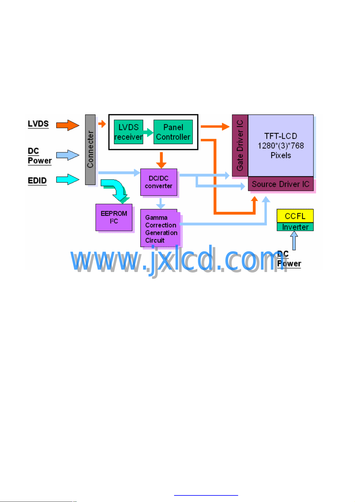
22..22 FFuunnccttiioonnaall BBlloocckk DDiiaaggrraamm
The following diagram shows the functional block of the 14.1 inches Color TFT/LCD Module:
www.jxlcd.com
(C) Copyright AU Optronics
Dec., 2002 All Rights Reserved. B141XG09 V2
No Reproduction and Redistribution Allowed.
6/26
www.jxlcd.com
PDF created with FinePrint pdfFactory trial version www.pdffactory.com
Page 7
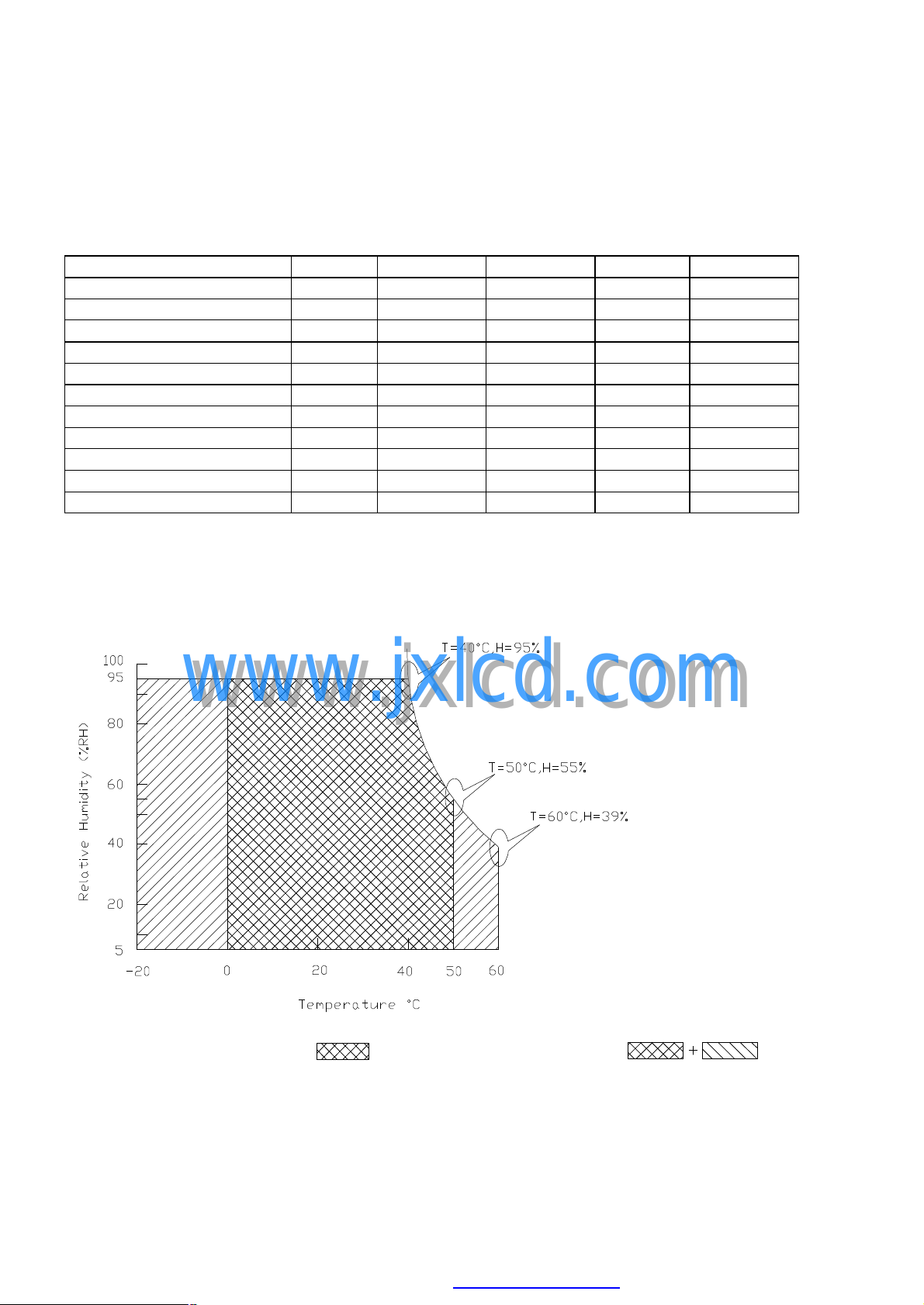
3.0 Absolute Maximum Ratings
Half sine
Absolute maximum ratings of the module is as following:
Item Symbol Min Max Unit Conditions
Logic/LCD Drive Voltage VDD -0.3 +4.0 [Volt]
Input Voltage of Signal Vin -0.3 VDD+0.3 [Volt]
LVDS Input Voltage VLVDS in -0.3 +2.6 [Volt]
CCFL Current ICFL - 6.5 [mA] rms
CCFL Ignition Voltage Vs - 1160(25oC) Vrms Note 1
Operating Temperature TOP 0 +50 [oC] Note 2
Operating Humidity HOP 5 95 [%RH] Note 2
Storage Temperature TST -20 +60 [oC] Note 2
Storage Humidity HST 5 95 [%RH] Note 2
Vibration 1.5 ,10-500
Shock 220 , 2 [G ms]
Note 1 : Duration = 50msec
Note 2 : Maximum Wet-Bulb should be 39℃ and No condensation.
Wet bulb temperature chart
Twb=39° C
[G Hz]
www.jxlcd.com
www.jxlcd.com
Operating Range Storage Range
(C) Copyright AU Optronics
Dec., 2002 All Rights Reserved. B141XG09 V2
No Reproduction and Redistribution Allowed.
7/26
PDF created with FinePrint pdfFactory trial version www.pdffactory.com
Page 8

4.0 Optical Characteristics
The optical characteristics are measured under stable conditions as follows under 25℃ condition:
Item Unit Conditions Min. Typ. Max. Note
Viewing Angle
CR: Contrast Ratio
Uniformity 5 Points 1.2
Uniformity 13 Points 1.5
Contrast ratio 300 - - 6
Response Time [msec] Rising - 10 15
[msec] Falling - 15 20
Color / Chromaticity Red x
Coordinates Red y
(CIE 1931) Green x
www.jxlcd.com
Blue x 0.150
Blue y 0.130
White x 0.313
www.jxlcd.com
[degree]
[degree]
[degree]
[degree]
Horizontal (Right)
CR = 10 (Left)
Vertical (Upper)
CR = 10 (Lower)
Green y
40
40
10
30
0.580
0.340
0.310
0.550
-
-
-
-
-
3,7
-
-
2
5
3,7
White Luminance
CCFL 6.0mA
(C) Copyright AU Optronics
Dec., 2002 All Rights Reserved. B141XG09 V2
No Reproduction and Redistribution Allowed.
8/26
[cd/m2] 5 points average 160 200 - 1,3,4
White y 0.329
PDF created with FinePrint pdfFactory trial version www.pdffactory.com
Page 9
Note 1: 5 & 13 points position (Display area: 285.7mm x 214.3mm)
δ
=
Maximum Brightness of thirteen points
Maximum Brightness of five (1,2,3,4,5) points
δ
=
Minimum Brightness of five (1,2,3,4,5) points
10mm10mm
6
10mm
9
10mm
11
Note 2: Definition of white uniformity:
www.jxlcd.com
White uniformity is defined as the following with five/thirteen measurements (1~13) at Figure in Note (1). .
www.jxlcd.com
1 2
3
7
5
4
12
512256
768
10
13
8
192
384
576
Note 3: Measurement method
The LCD module should be stabilized at given temperature for 30 minutes to avoid abrupt temperature change
during measuring. In order to stabilize the luminance, the measurement should be executed after lighting Backlight
for 30 minutes in a stable, wi ndless and dark room.
(C) Copyright AU Optronics
Dec., 2002 All Rights Reserved. B141XG09 V2
No Reproduction and Redistribution Allowed.
9/26
W5
W13
Minimum Brightness of thirteen points
PDF created with FinePrint pdfFactory trial version www.pdffactory.com
Page 10

Photodetector
(BM-5A,BM-7 or equivalent)
Field=2°
LCD Panel
Center of the screen
Note 4: Definition of Average Luminance of White (YL):
Measure the luminance of gray level 63 at 5 points,YL = [L (1)+ L (2)+ L (3)+ L (4)+ L (5)] / 5
L (x) is corresponding to the luminance of the point X at Figure in Note (1).
Note 5: Definition of response time:
The output signals of BM-7 or equivalent are measured when the input signals are changed from “Black” to “White”
(falling time) and from “White” to “Black” (rising time), respectively. The response time interval between the 10% and
90% of amplitudes. Refer to figure as below.
www.jxlcd.com
www.jxlcd.com
50 cm
TFT-LCD Module
(C) Copyright AU Optronics
Dec., 2002 All Rights Reserved. B141XG09 V2
No Reproduction and Redistribution Allowed.
10/26
PDF created with FinePrint pdfFactory trial version www.pdffactory.com
Page 11

"Black"
Contrast ratio (CR)=
Brightness on the “White” state
Brightness on the “Black” state
100%
S
i
90%
g
n
a
l
(
R
e
l
a
t
i
v
e
v
a
l
u
10%
e
)
0%
Note 6. Definition of contrast ratio:
Contrast ratio is calculated with the following formula.
Note 7. Definition of viewing angle
Viewing angle is the measurement of contrast ratio ≧10, at the screen center, over a 180° horizontal and
180° vertical range (off-normal viewing angles). The 180 ° viewing angle range is broken down as follows; 90° (θ)
horizontal left and right and 90° (Φ) vertical, high (up) and low (down). The measurement direction is typically
perpendicular to the display surface with the screen rotated about its center to develop the desired measurement
viewing angle.
www.jxlcd.com
www.jxlcd.com
Tr
Tf
"White""White"
(C) Copyright AU Optronics
Dec., 2002 All Rights Reserved. B141XG09 V2
No Reproduction and Redistribution Allowed.
11/26
PDF created with FinePrint pdfFactory trial version www.pdffactory.com
Page 12

5.0 Signal Interface
55..11 CCoonnnneeccttoorrss
Physical interface is described as for the connector on module.
These connectors are capable of accommodating the following signals and will be following components.
Connector Name / Designation For Signal Connector
Manufacturer JAE
Type / Part Number FI-XB30SL-HF10
Mating Housing/Part Number FI-X30H
Mating Contact/Part Number FI-XC3-1-15000
Connector Name / Designation For Lamp Connector
Manufacturer JST
Type / Part Number BHSR-02VS-1
Mating Type / Part Number SM02B-BHSS-1-TB
www.jxlcd.com
www.jxlcd.com
(C) Copyright AU Optronics
Dec., 2002 All Rights Reserved. B141XG09 V2
No Reproduction and Redistribution Allowed.
12/26
PDF created with FinePrint pdfFactory trial version www.pdffactory.com
Page 13

55..22 SSiiggnnaall PPiinn
Pin# Signal Name Pin# Signal Name
1 GND 2 VDD
3 VDD 4 V
5 BIST TEST 6 CLK
7 DATA
9 RxIN0+ 10 GND
11 RxIN1- 12 RxIN1+
13 GND 14 RxIN215 RxIN2+ 16 GND
17 RxCLKIN- 18 RxCLKIN+
19 GND 20~30 NC
55..33 SSiiggnnaall DDeessccrriippttiioonn
The module uses a LVDS receiver embedded in AUO’s ASIC. LVDS is a differential signal technology for LCD
interface and high-speed data transfer device.
RxIN0-, RxIN0+ LVDS differential data input(Red0-Red5, Green0)
www.jxlcd.com
www.jxlcd.com
Signal Name Description
8 RxIN0-
EDID
EDID
EDID
RxIN1-, RxIN1+ LVDS differential data input(Green1-Green5, Blue0-Blue1)
RxIN2-, RxIN2+ LVDS differential data input(Blue2-Blue5, DSPTMG)
RxCLKIN-, RxCLKIN0+ LVDS differential clock input
VDD +3.3V Power Supply
GND Ground
Note: Input signals shall be in low status when VDD is off.
(C) Copyright AU Optronics
Dec., 2002 All Rights Reserved. B141XG09 V2
No Reproduction and Redistribution Allowed.
13/26
PDF created with FinePrint pdfFactory trial version www.pdffactory.com
Page 14

Internal circuit of LVDS inputs are as following.
Signal Name Description
+RED5
+RED4
+RED3
+RED2
+RED1
+RED0
+GREEN 5
+GREEN 4
+GREEN 3
+GREEN 2
+GREEN 1
+GREEN 0
+BLUE 5
+BLUE 4
+BLUE 3
+BLUE 2
+BLUE 1
+BLUE 0
-DTCLK Data Clock
DSPTMG Display Timing This signal is strobed at the falling edge of
Note: Output signals from any system shall be low or Hi-Z state when VDD is off.
Red Data 5 (MSB)
Red Data 4
Red Data 3
Red Data 2
Red Data 1
Red Data 0 (LSB)
Red-pixel Data
Green Data 5 (MSB)
Green Data 4
Green Data 3
Green Data 2
Green Data 1
Green Data 0 (LSB)
Green-pixel Data
Blue Data 5 (MSB)
Blue Data 4
Blue Data 3
Blue Data 2
Blue Data 1
Blue Data 0 (LSB)
Blue-pixel Data
www.jxlcd.com
www.jxlcd.com
Red-pixel Data
Each red pixel's brightness data consists of these 6 bits
pixel data.
Green-pixel Data
Each green pixel's brightness data consists of these 6 bits
pixel data.
Blue-pixel Data
Each blue pixel's brightness data consists of these 6 bits
pixel data.
The typical frequency is 65.0 MHz. The signal is used to
strobe the pixel data and DSPTMG signals. All pixel data
shall be valid at the falling edge when the DSPTMG signal
is high.
-DTCLK. When the signal is high, the pixel data shall be
valid to be displayed.
55..44 SSiiggnnaall EElleeccttrriiccaall CChhaarraacctteerriissttiiccss
Input signals shall be in low status when VDD is off.
It is recommended to refer the specifications of SN75LVDS86DGG (Texas Instruments) in detail.
Signal electrical characteristics are as follows;
Symbol Parameter Condition Min Max Unit
VTH
VTL
Differential Input High
Threshold
Differential Input Low
Threshold
Vcm=+1.2V
100
Vcm=+1.2V
-100
(C) Copyright AU Optronics
Dec., 2002 All Rights Reserved. B141XG09 V2
No Reproduction and Redistribution Allowed.
14/26
PDF created with FinePrint pdfFactory trial version www.pdffactory.com
[mV]
[mV]
Page 15

LVDS Macro AC characteristics are as follows:
Clock Frequency (F) 50MHz 68MHz
Data Setup Time (Tsu) 600ps
Data Hold Time (Thd) 600ps
F
T
Input Clock
Input Data
Min. Max.
ThdTsu
www.jxlcd.com
55..55 SSiiggnnaall ffoorr LLaammpp ccoonnnneeccttoorr
www.jxlcd.com
Pin # Signal Name
1 Lamp High Voltage
2 Lamp Low Voltage
(C) Copyright AU Optronics
Dec., 2002 All Rights Reserved. B141XG09 V2
No Reproduction and Redistribution Allowed.
15/26
PDF created with FinePrint pdfFactory trial version www.pdffactory.com
Page 16
Brightness Adjust (Lamp
55..66 IInnvveerrtteerr CChhaarraacctteerriissttiicc
. Item Symbol Condition Min. Typ. Max.
1 Input Voltage Vin 7.5 14.4 21 V
2 Input Current Iin Vin=7.5V,SMData=00H 600 660 720 mA
3 Input Power Pin Vin=21V,SMData=00H --- 5.25 --- W
Input Signal Level for
4
5
6
7 Output Voltage Vout SMData=00H 621 690 759 V(rms)
5VSUS,5VALW
Backlight ON FPVEE=Hi 2.0 - 5.25
ON/OFF Control OFF FPVEE=Lo -0.3 - 0.8 V
Current Control)
4.85 5 5.2 V
SMData Control by SMBus FFH - 00H
Uint
V
-
www.jxlcd.com
www.jxlcd.com
8 Output Current
9 Frequency Freq Vin=7.5~21V 45 55 65 KHz
10 Output Power Pout Vin=21V,SMData=00H --- 4.14 4.6 W
11 Open Lamp Voltage Vopen No Load 1400 -- 1800 V(rms)
12 Striking Time Ts Vin=7.5V~21V 0.6 1 1.4 Sec
13 Efficiency η
(C) Copyright AU Optronics
Dec., 2002 All Rights Reserved. B141XG09 V2
No Reproduction and Redistribution Allowed.
16/26
Duty cycle
Iout (Max)
Vin(7.5V~21V)SMData=FFH Ta=25
℃, after running 30 min.
Vin(7.5V~21V)SMData=00H Ta=25
℃, after running 30 min.
Vin=7.5V, Iout=Max.
Load=110Kohm//15 p farad
(Dummy Load)
6 10 14
5.5 6.0 6.5 mA(rms)
80 --- --- %
% duty
cycle
PDF created with FinePrint pdfFactory trial version www.pdffactory.com
Page 17
6.0 Pixel Format Image
Following figure shows the relationship of the input signals and LCD pixel format.
0 1 1022 1023
1st Line
768th Line
R G B R G B
R G B R G B
www.jxlcd.com
www.jxlcd.com
7.0 Parameter guide line for CCFL Inverter
R G B R G B
R G B R G B
Parameter Min DP-1 Max
White Luminance
5 points average
CCFL current(ICFL)
Linear mode
CCFL Frequency(FCFL)
CCFL Ignition Voltage(Vs)
CCFL Voltage (Reference)
(VCFL)
CCFL Power consumption
(PCFL)
Note 1: DP-1 are AUO recommended Design Points.
*1 All of characteristics listed are measured under the condition using the AUO Test inverter.
(C) Copyright AU Optronics
Dec., 2002 All Rights Reserved. B141XG09 V2
No Reproduction and Redistribution Allowed.
17/26
160 200
2.0 6.0 6.5 [mA] rms
50 60 70 [KHz]
650
3.9
1400 [Volt] rms
Units Condition
[cd/m2 ]
[Volt] rms
[Watt]
(Ta=25℃)
(Ta=25℃)
Note 2
(Ta=25℃)
Note 3
(Ta= 0℃)
Note 4
(Ta=25℃)
Note 5
(Ta=25℃)
Note 5
PDF created with FinePrint pdfFactory trial version www.pdffactory.com
Page 18

*2 In case of using an inverter other than listed, it is recommended to check the inverter carefully. Sometimes,
interfering noise stripes appear on the screen, and substandard luminance or flicker at low power may happen.
*3 In designing an inverter, it is suggested to check safety circuit ver carefully. Impedance of CCFL, for instance,
becomes more than 1 [M ohm] when CCFL is damaged.
*4 Generally, CCFL has some amount of delay time after applying start-up voltage. It is recommended to keep on
applying start-up voltage for 1 [Sec] until discharge.
*5 The CCFL inverter operating frequency must be carefully chosen so that no interfering noise stripes on the
screen were induced.
*6 Reducing CCFL current increases CCFL discharge voltage and generally increases CCFL discharge
frequency. So all the parameters of an inverter should be carefully designed so as not to produce too much
leakage current from high-voltage output of the inverter.
Note 2: It should be employed the inverter, which has “Duty Dimming”, if ICCFL is less than 4mA.
Note 3: The CCFL inverter operating frequency should be carefully determined to avoid interference between
inverter and TFT LCD.
Note 4: The inverter open voltage should be designed larger than the lamp starting voltage at T=0oC, otherwise
backlight may be blinking for a moment after turning on or not be able to turn on. The open voltage should be
measured after ballast capacitor. If an inverter has shutdown function it should keep its open voltage. for
longer than 1 second even if lamp connector is open.
Note 5: Calculator value for reference (ICFL×VCFL=PCFL)
www.jxlcd.com
www.jxlcd.com
(C) Copyright AU Optronics
Dec., 2002 All Rights Reserved. B141XG09 V2
No Reproduction and Redistribution Allowed.
18/26
PDF created with FinePrint pdfFactory trial version www.pdffactory.com
Page 19

8.0 Interface Timings
Basically, interface timings should match the VESA 1024x768 /60Hz (VG901101) manufacturing guide line timing.
88..11 TTiimmiinngg CChhaarraacctteerriissttiiccss
Symbol Description Min Typ Max Unit
fdck DTCLK Frequency 50.0 65.00 68.00 [MHz]
tck DTCLK cycle time 15.38 [nsec]
tx X total time 1054 1344 2048 [tck]
tacx X active time 1024 [tck]
tbkx X blank time 30 320 1024 [tck]
ty Y total time 773 806 1024 [tx]
tacy Y active time 768 [tx]
Frame rate 60 [Hz]
88..22 TTiimmiinngg DDeeffiinniittiioonn
www.jxlcd.com
www.jxlcd.com
(C) Copyright AU Optronics
Dec., 2002 All Rights Reserved. B141XG09 V2
No Reproduction and Redistribution Allowed.
19/26
PDF created with FinePrint pdfFactory trial version www.pdffactory.com
Page 20
9.0 Power Consumption
Input power specifications are as follows;
Symbol Parameter Min Typ Max Units
Module
VDD
PDD VDD Power 1.2 [Watt] All Black Pattern
PDD Max VDD Power max 1.65 [Watt] Max Pattern Note
IDD IDD Current 350 mA 64 Grayscale Pattern
IDD Max IDD Current max 450 mA
Lamp
ICFL CCFL current 2.0 6.0 6.5
VCFL
PCFL
Total Power
Consumption
Logic/LCD Drive
Voltage
CCFL Voltage
(Reference)
CCFL Power
consumption
5.1 Watt (w/o Inverter, All black pattern)@LCM circuit 1.2 Watt(typ.),B/L input 3.9
Watt(typ.)
3.0 3.3 3.6 [Volt] Load Capacitance 20uF
[mA]
rms
650
3.9
[Volt]
rms
[Watt]
Vertical stripe line Pattern
Note
(Ta=25℃)
(Ta=25℃)
(Ta=25℃)
Condition
www.jxlcd.com
Note : VDD=3.3V
(C) Copyright AU Optronics
Dec., 2002 All Rights Reserved. B141XG09 V2
No Reproduction and Redistribution Allowed.
20/26
www.jxlcd.com
PDF created with FinePrint pdfFactory trial version www.pdffactory.com
Page 21
T3 T2
T5
T1
T6
T7
10.0 Power ON/OFF Sequence
VDD power and lamp on/off sequence is as follows. Interface signals are also shown in the chart. Signals
from any system shall be Hi-Z state or low level when VDD is off.
Sequence of Power-on/off and signal-on/off
Power Supply VDD
LVDS Interface
Backlight On
Apply the lamp voltage within the LCD operating range. When the backlight turns on before the LCD
operation or the LCD turns off before the backlight turns off, the display may momentarily become abnormal.
0.1VDD
www.jxlcd.com
www.jxlcd.com
0.9VDD
0.9VDD
0.1VDD
0ms≦T1
0ms≦T2≦50ms
0ms≦T3<50ms
100ms≦T4
200ms≦T5
0ms≦T6
0ms≦T7
(C) Copyright AU Optronics
Dec., 2002 All Rights Reserved. B141XG09 V2
No Reproduction and Redistribution Allowed.
21/26
PDF created with FinePrint pdfFactory trial version www.pdffactory.com
Page 22
11.0 Reliability /Safety Requirement
/1 Hr min. power on/off per 5 minutes, 5
/1 Hr min. power on/off per 5 minutes, 5
to 500
in each of three
operation
1111..11 RReelliiaabbiilliittyy TTeesstt CCoonnddiittiioonnss
Items Required Condition
Temperature Humidity Bias
High Temperature Operation
Low Temperature Operation
Continuous Life
On/Off Test
Hot Storage
Cold Storage
Thermal Shock Test
Hot Start Test
Cold Start Test
Shock Test (Non-Operating)
Vibration Test (Non-Operating)
ESD
Altitude Test
Maximum Side Mount Torque
www.jxlcd.com
www.jxlcd.com
40℃/90%,300Hr
50℃/Dry,300Hr
0℃,500Hr
25℃ ,2000 hours
ON/30 sec. OFF/30sec., 30,000 cycles
60℃/40% RH ,240 hours
-20℃/50% RH ,240 hours
-20℃/30 min ,60℃/30 min 100cycles
50℃
times
0℃
times
240G, 2ms, Half-sine wave
Sinusoidal vibration, 1.5G zero-to-peak, 10
Hz, 0.5 octave/minute; 0.5hr
mutually perpendicular axes.
Contact : operation ±8KV / non-
±10KV
Air : operation ±15KV / non-operation ±20KV
10000 ft / operation / 8Hr
30000ft / non-operation / 24r
2.5kgf.cm .
1111..22 SSaaffeettyy
UL 60950
(C) Copyright AU Optronics
Dec., 2002 All Rights Reserved. B141XG09 V2
No Reproduction and Redistribution Allowed.
22/26
PDF created with FinePrint pdfFactory trial version www.pdffactory.com
Page 23

12.0 Packing dimension
14.1” LCD Module
ESD bag
20pcs LCD Module
Carton
Carton Label Position
www.jxlcd.com
www.jxlcd.com
(C) Copyright AU Optronics
Dec., 2002 All Rights Reserved. B141XG09 V2
No Reproduction and Redistribution Allowed.
23/26
PDF created with FinePrint pdfFactory trial version www.pdffactory.com
Page 24
13.0 Mechanical Characteristics
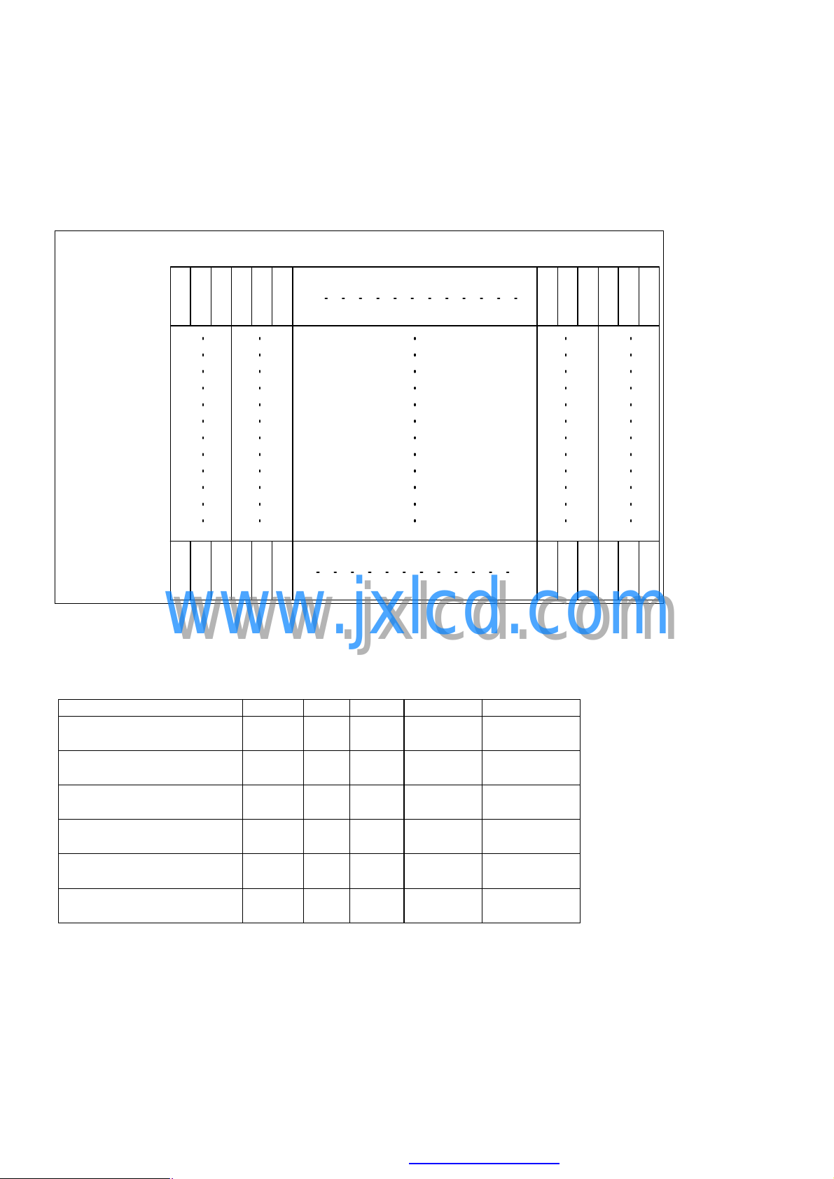
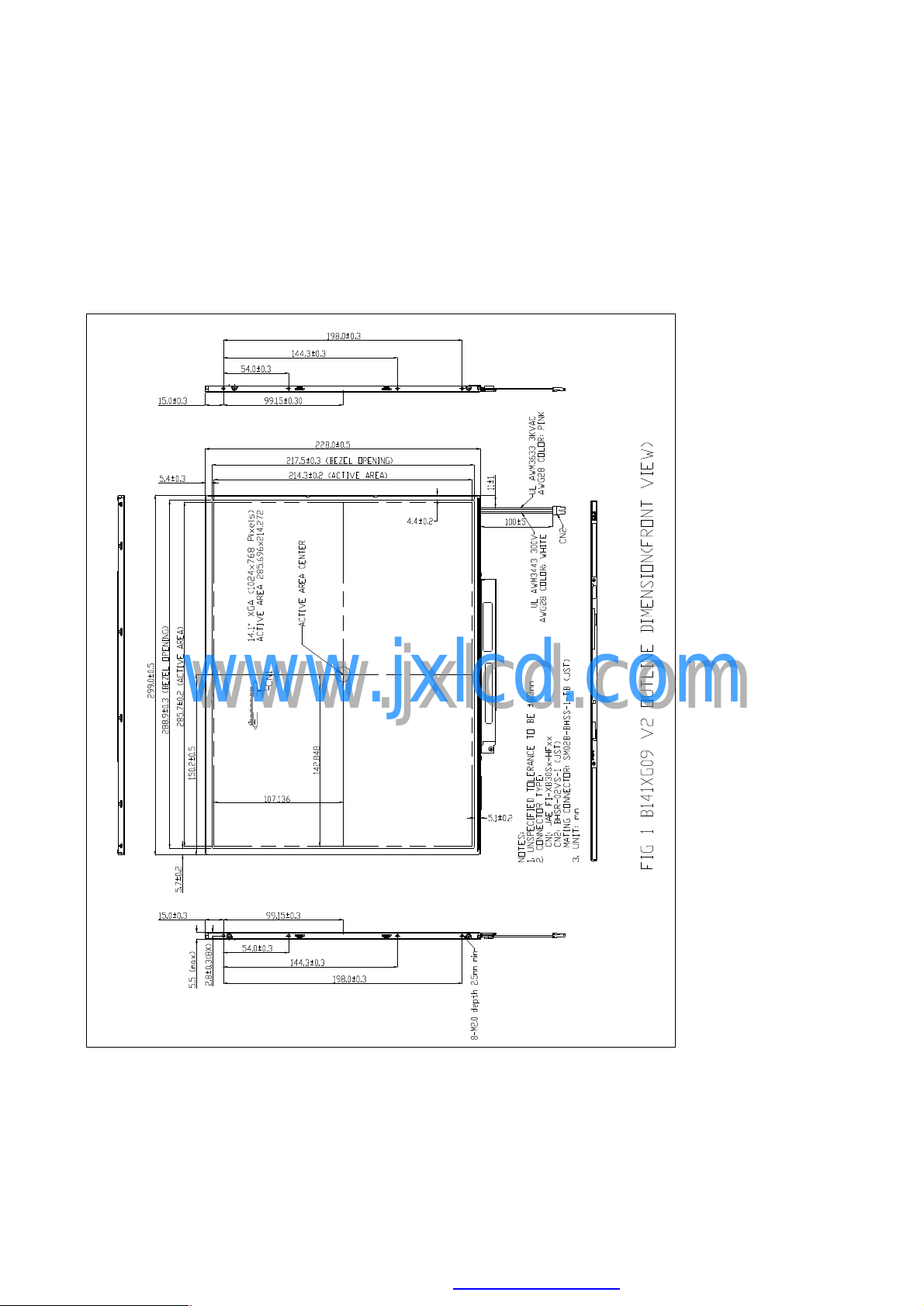
1133..11 LLCCMM OOuuttlliinnee ddiimmeennssiioonn ((FFrroonntt VViieeww))
www.jxlcd.com
www.jxlcd.com
(C) Copyright AU Optronics
Dec., 2002 All Rights Reserved. B141XG09 V2
No Reproduction and Redistribution Allowed.
24/26
PDF created with FinePrint pdfFactory trial version www.pdffactory.com
Page 25
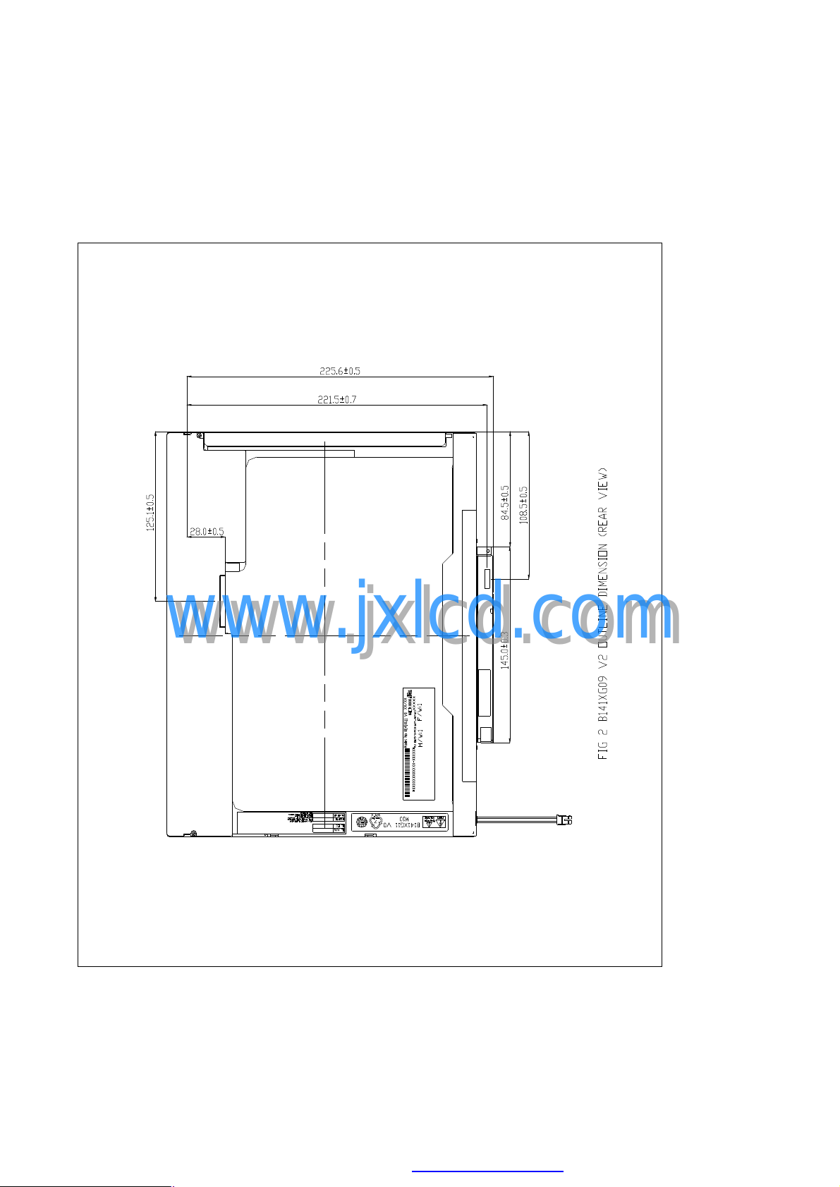
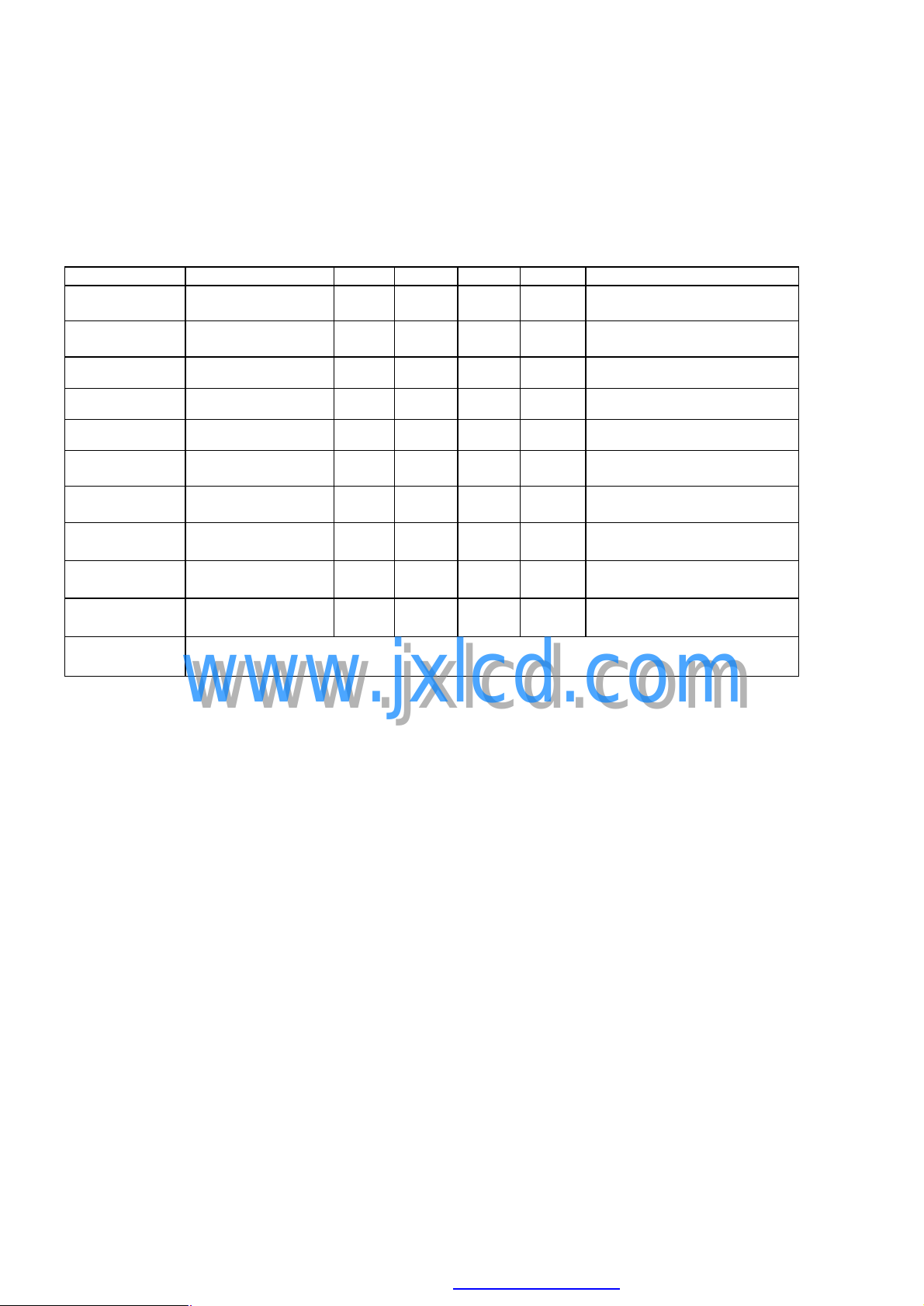
1133..22 LLCCMM OOuuttlliinnee DDiimmeennssiioonn ((RReeaarr VViieeww))
www.jxlcd.com
www.jxlcd.com
(C) Copyright AU Optronics
Dec., 2002 All Rights Reserved. B141XG09 V2
No Reproduction and Redistribution Allowed.
25/26
PDF created with FinePrint pdfFactory trial version www.pdffactory.com
Page 26

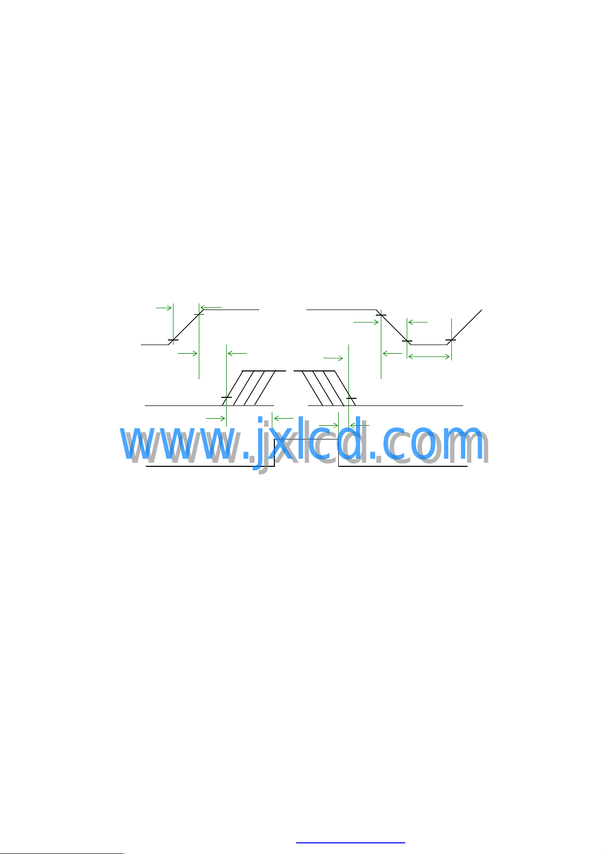
1133..33 SSccrreeww HHoollee DDeepptthh aanndd CCeenntteerr PPoossiittiioonn
Screw hole minimum depth, from side surface =2.5 mm (See drawing)
Screw hole center location, from front surface = 2.8 ± 0.3mm (See drawing)
Screw maximum length = 2.3 mm (See drawing)
Screw Torque: Maximum2.5 kgf-cm
www.jxlcd.com
www.jxlcd.com
(C) Copyright AU Optronics
Dec., 2002 All Rights Reserved. B141XG09 V2
No Reproduction and Redistribution Allowed.
26/26
PDF created with FinePrint pdfFactory trial version www.pdffactory.com
 Loading...