

Page 1

Product Specification
) Preliminary Specifications
( V
( ) Final Specifications
Module 14.1” WXGA Color TFT-LCD with LED Backlight design
AU OPTRONICS CORPORATION
Model Name
Note ( )
Customer Date
www.jxlcd.com
www.jxlcd.com
Checked &
Approved by
B141EW05 V2
LED Backlight design
Date
Approved by Date
Beyond Yang
Prepared by
09/25/2008
Note: This Specification is subject to change without
notice.
B141EW05 V2 Document Version: 0.5
Jeff Hou
NBBU Marketing Division /
AU Optronics corporation
09/25/2008
1 of 35
Page 2

Product Specification
AU OPTRONICS CORPORATION
Contents
1. Handling Precautions .............................................................. 4
2. General Description ................................................................ 5
2.1 General Specification ..........................................................................................................................5
2.2 Optical Characteristics ........................................................................................................................6
3. Functional Block Diagram ..................................................... 11
4. Absolute Maximum Ratings................................................... 12
4.1 Absolute Ratings of TFT LCD Module.............................................................................................12
4.2 Absolute Ratings of Backlight Unit...................................................................................................12
4.3 Absolute Ratings of Environment .....................................................................................................12
5. Electrical characteristics ....................................................... 13
5.1 TFT LCD Module..............................................................................................................................13
5.2 Backlight Unit ...................................................................................................................................15
6. Signal Characteristic ............................................................. 16
6.1 Pixel Format Image ...........................................................................................................................16
6.2 The input data format ........................................................................................................................17
6.3 Signal Description/Pin Assignment...................................................................................................18
6.4 Interface Timing ................................................................................................................................22
7. Connector Description........................................................... 24
7.1 TFT LCD Module..............................................................................................................................24
www.jxlcd.com
8. LED Driving Specification ...................................................... 25
8.1 Connector Description.......................................................................................................................25
8.2 Pin Assignment..................................................................................................................................25
www.jxlcd.com
9. Vibration and Shock Test ...................................................... 26
9.1 Vibration Test ....................................................................................................................................26
9.2 Shock Test Spec:................................................................................................................................26
10. Reliability............................................................................ 27
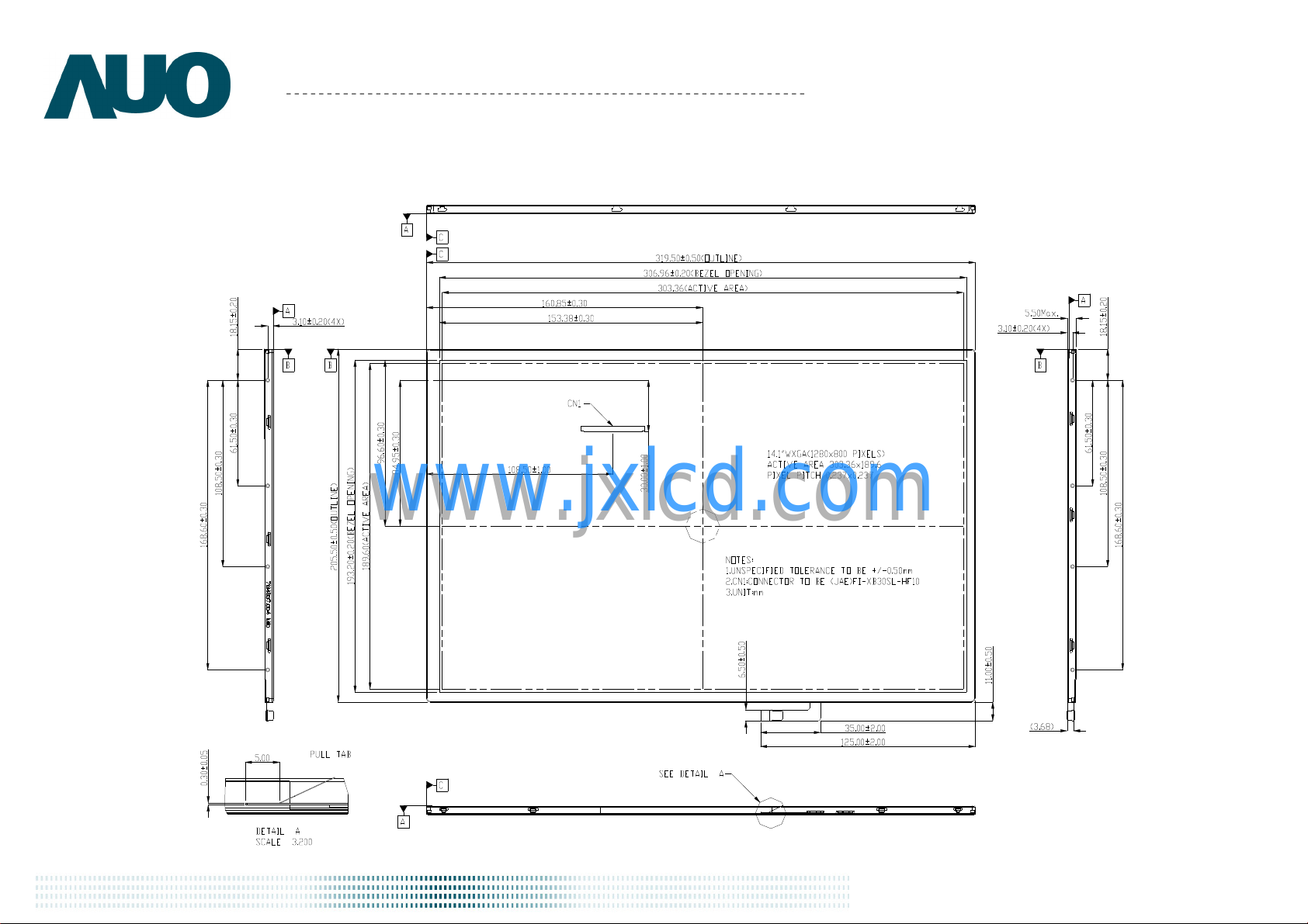
11. Mechanical Characteristics.................................................. 28
11.1 LCM Outline Dimension.................................................................................................................28
11.2 Screw Hole Depth and Center Position ...........................................................................................30
12. Shipping and Package ......................................................... 31
12.1 Shipping Label Format....................................................................................................................31
12.2 Carton package................................................................................................................................32
11.3 Shipping package of palletizing sequence.......................................................................................32
13. Appendix: EDID description ................................................ 33
B141EW05 V2 Document Version: 0.5
2 of 35
Page 3

Product Specification
AU OPTRONICS CORPORATION
Record of Revision
Version and Date Page
0.1 2008/5/16 All First Edition for Customer
0.2 2008/5/26 12
0.3 2008/6/9 29,30 Update drawing Update drawing
0.4 2008/8/14 32 Update Label Update Label
0.5 2008/9/25 6 Update response time and color
20,28 Update drawing
22 Update clock frequency =70.5
33 Update EDID
www.jxlcd.com
www.jxlcd.com
LED Light bar Driving
Old description New Description Remark
Update LED Light bar Driving
coodinates
= 25.2 (Row Output)
B141EW05 V2 Document Version: 0.5
3 of 35
Page 4

Product Specification
1. Handling Precautions
1) Since front polarizer is easily damaged, pay attention not to scratch it.
2) Be sure to turn off power supply when inserting or disconnecting from input connector.
3) Wipe off water drop immediately. Long contact with water may cause discoloration or
spots.
4) When the panel surface is soiled, wipe it with absorbent cotton or other soft cloth.
5) Since the panel is made of glass, it may break or crack if dropped or bumped on hard
surface.
6) Since CMOS LSI is used in this module, take care of static electricity and insure
human earth when handling.
7) Do not open nor modify the Module Assembly.
8) Do not press the reflector sheet at the back of the module to any directions.
9) At the insertion or removal of the Signal Interface Connector, be sure not to rotate nor
tilt the Interface Connector of the TFT Module.
AU OPTRONICS CORPORATION
11) After installation of the TFT Module into an enclosure (Notebook PC Bezel, for
example), do not twist nor bend the TFT Module even momentary. At designing the
enclosure, it should be taken into consideration that no bending/twisting forces are
applied to the TFT Module from outside. Otherwise the TFT Module may be
damaged.
12) Small amount of materials having no flammability grade is used in the LCD module. The
LCD module should be supplied by power complied with requirements of Limited Power
Source (IEC60950 or UL1950), or be applied exemption.
13) Disconnecting power supply before handling LCD modules, it can prevent electric shock, DO
NOT TOUCH the electrode parts, cables, connectors and LED circuit part of TFT module
that a LED light bar build in as a light source of back light unit. High voltage is supplied to
these parts when power turn on.
www.jxlcd.com
www.jxlcd.com
B141EW05 V2 Document Version: 0.5
4 of 35
Page 5

Product Specification
(Note1)
Thickness
2. General Description
B141EW05 V2 is a Color Active Matrix Liquid Crystal Display composed of a TFT LCD panel,
and LED backlight system. The screen format is intended to support the WXGA (1280(H) x
800(V)) screen and 262k colors (RGB 6-bits data driver) . All input signals are LVDS interface
compatible.
B141EW05 V2 is designed for a display unit of notebook style personal computer and industrial
machine.
AU OPTRONICS CORPORATION
2.1 General Specification
The following items are characteristics summary on the table at 25 ℃ condition:
Items Unit Specifications
Screen Diagonal [mm] 357.7 (14.1W”)
Active Area [mm] 303.36 X 189.6
Pixels H x V 1280x3(RGB) x 800
Pixel Pitch [mm] 0.237
Pixel Format B.G.R. Vertical Stripe
Display Mode Normally White
www.jxlcd.com
White Luminance (I
Note: I
Luminance Uniformity 1.25 max. (5 points)
Contrast Ratio 500 typ
LED
www.jxlcd.com
is LED current
LED
=20mA)
[cd/m2] 220 typ. (5 points average)
187 min. (5 points average)
Response Time [ms] 8 typ / 12 Max
Nominal Input Voltage VDD [Volt] +3.3 typ.
Power Consumption [Watt] 4.4 max. (Include Logic and Blu power)
Weight [Grams] 385 max.
Physical Size without inverter,
bracket.
Electrical Interface 1 channel LVDS
Surface Treatment Glare,
B141EW05 V2 Document Version: 0.5
[mm]
Min. Typ. Max.
Length 319 319.5 320
Width 205 205.5 206
4.8 - 5.5
5 of 35
Page 6

Product Specification
RoHS Compliance
Support Color 262K colors ( RGB 6-bit )
AU OPTRONICS CORPORATION
Temperature Range
Operating
Storage (Non-Operating)
RoHS Compliance
[oC]
[oC]
0 to +50
-20 to +65
2.2 Optical Characteristics
The optical characteristics are measured under stable conditions at 25℃ (Room Temperature) :
Item Symbol
White Luminance
I
LED
=20mA
Viewing Angle
Luminance
Uniformity
Luminance
Uniformity
Contrast Ratio CR
Cross talk %
Response Time
Color /
Chromaticity
Coodinates
www.jxlcd.com
www.jxlcd.com
Red x
Red y
Green x
Green y
Blue x
Blue y
White x
White y
θθθθR
θθθθL
ψψψψH
ψψψψL
δδδδ5P
δδδδ
13P
Tr Rising
Tf Falling
TRT Rising + Falling
Conditions Min. Typ. Max.
5 points average
Horizontal (Right)
CR = 10 (Left)
Vertical (Upper)
CR = 10 (Lower)
5 Points
13 Points
300 400 -
4
CIE 1931
187 220 - cd/m
40
40
10
30
- - 1.25
- - 1.50
-
- 2 5
- 8 12
0.556 0.586 0.616
0.316 0.346 0.376
0.311 0.341 0.371
0.546 0.576 0.606
0.127 0.157 0.187
0.090 0.120 0.150
0.283 0.313 0.343
0.299 0.329 0.359
45
45
15
35
6
-
-
-
-
10
Unit Note
2
1, 4, 5.
degree
4, 9
1, 3, 4
2, 3, 4
4, 6
4, 7
msec
4, 8
4
NTSC %
B141EW05 V2 Document Version: 0.5
- 45 -
6 of 35
Page 7

Product Specification
=
Maximum Brightness of thirteen points
Minimum Brightness of thirteen points
Maximum Brightness of five
points
=
Minimum Brightness of five points
Note 1: 5 points position (Ref: Active area)
H /4
H /4
AU OPTRONICS CORPORATION
W / 4 W / 4 W / 4 W / 4
W
1 2
H
H /4
H /4
Note 2: 13 points position (Ref: Active area)
W /4
1 0
1 0
H /4
www.jxlcd.com
www.jxlcd.com
H /4
H
H /4
1
6
3
4
W
W /4
4 5
W /4
2
7
5
W /4
1 0
3
8
9
H /4
1 0
1 1
1 2
Note 3: The luminance uniformity of 5 or13 points is defined by dividing the maximum luminance values by the
minimum test point luminance
δ
W5
1 0
1 3
δ
Note 4: Measurement method
B141EW05 V2 Document Version: 0.5
W13
7 of 35
Page 8
Product Specification
Field=2
°
Contrast ratio (CR)=
Brightness on the “White” state
Brightness on the “Black” state
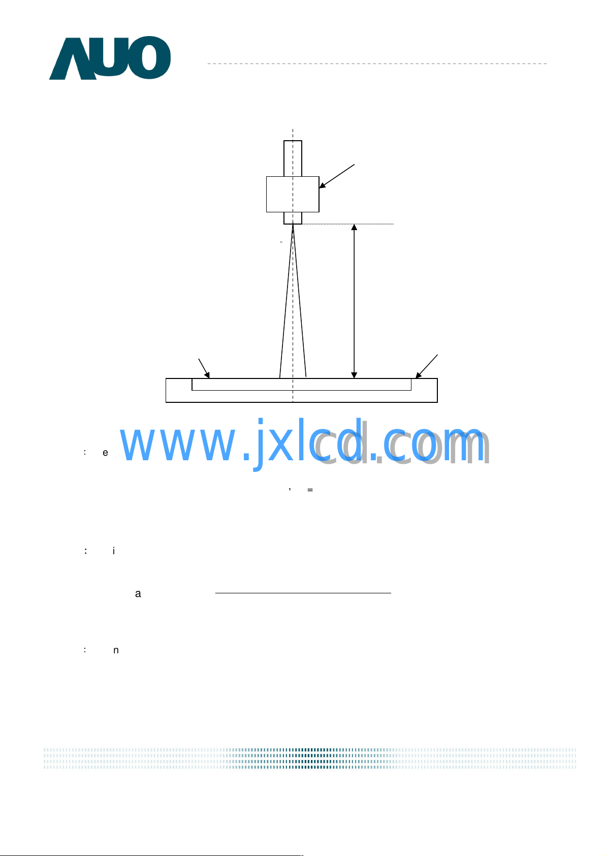
The LCD module should be stabilized at given temperature for 30 minutes to avoid abrupt temperature change
during measuring. In order to stabilize the luminance, the measurement should be executed after lighting Backlight
AU OPTRONICS CORPORATION
for 30 minutes in a stable, windless and dark room, , and it should be measured in the center of screen.
Photo detector
Note 5: Definition of Average Luminance of White (YL):
Measure the luminance of gray level 63 at 5 points,Y
L (x) is corresponding to the luminance of the point X at Figure in Note (1).
Note 6: Definition of contrast ratio:
Note 7: Definition of Cross Talk (CT)
CT = | YB – YA | / YA × 100 (%)
Where
YA = Luminance of measured location without gray level 0 pattern (cd/m2)
www.jxlcd.com
www.jxlcd.com
= [L (1)+ L (2)+ L (3)+ L (4)+ L (5)] / 5
L
Contrast ratio is calculated with the following formula.
B141EW05 V2 Document Version: 0.5
8 of 35
Page 9

Product Specification
YB = Luminance of measured location with gray level 0 pattern (cd/m2)
Note 8: Definition of response time:
The output signals of BM-7 or equivalent are measured when the input signals are changed from “Black” to
“White” (falling time) and from “White” to “Black” (rising time), respectively. The response time interval between the
10% and 90% of amplitudes. Refer to figure as below.
AU OPTRONICS CORPORATION
"Black"
100%
S
i
90%
g
n
a
l
(
R
e
l
a
t
i
v
e
v
a
l
u
e
)
www.jxlcd.com
www.jxlcd.com
10%
0%
Tr
Tf
"White""White"
B141EW05 V2 Document Version: 0.5
9 of 35
Page 10
Product Specification
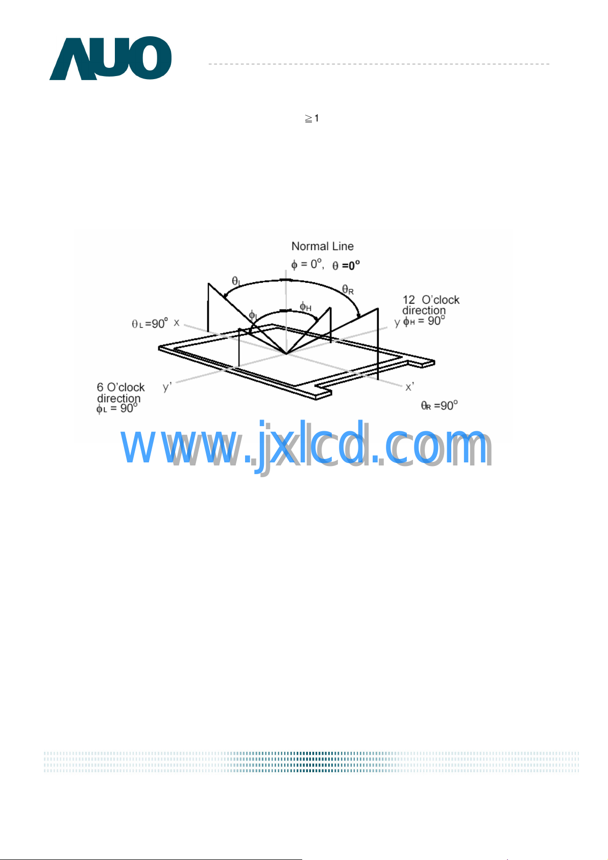
Note 9. Definition of viewing angle
Viewing angle is the measurement of contrast ratio ≧10, at the screen center, over a 180° horizontal and
180° vertical range (off-normal viewing angles). The 180° viewing angle range is broken down as follows; 90° (θ)
horizontal left and right and 90° (Φ) vertical, high (up) and low (down). The measurement direction is typically
perpendicular to the display surface with the screen rotated about its center to develop the desired measurement
viewing angle.
AU OPTRONICS CORPORATION
www.jxlcd.com
www.jxlcd.com
B141EW05 V2 Document Version: 0.5
10 of 35
Page 11
Product Specification
L
ight Bar
Connector(
FPC 12PIN
) LCD Connector(
30
pin)
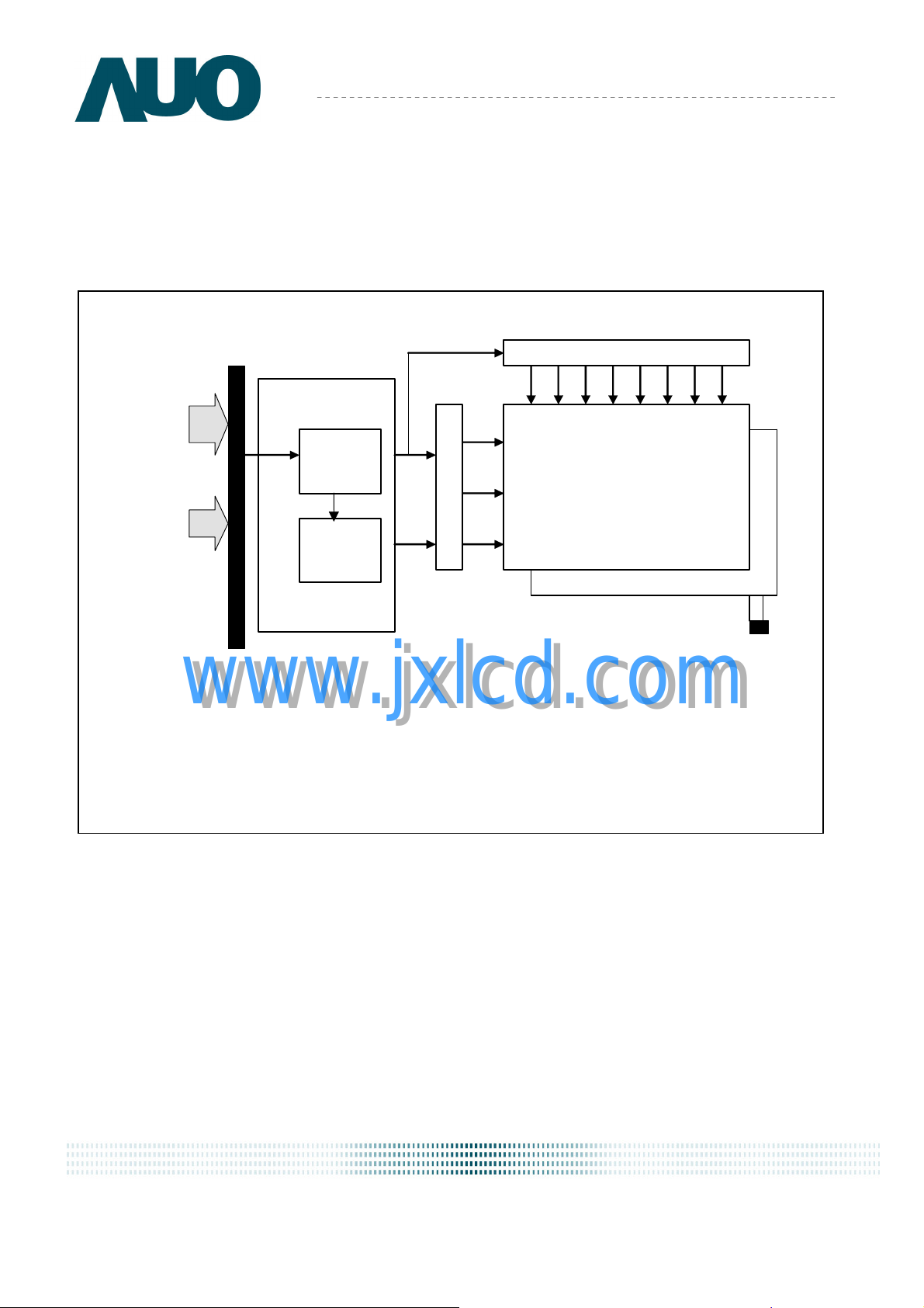
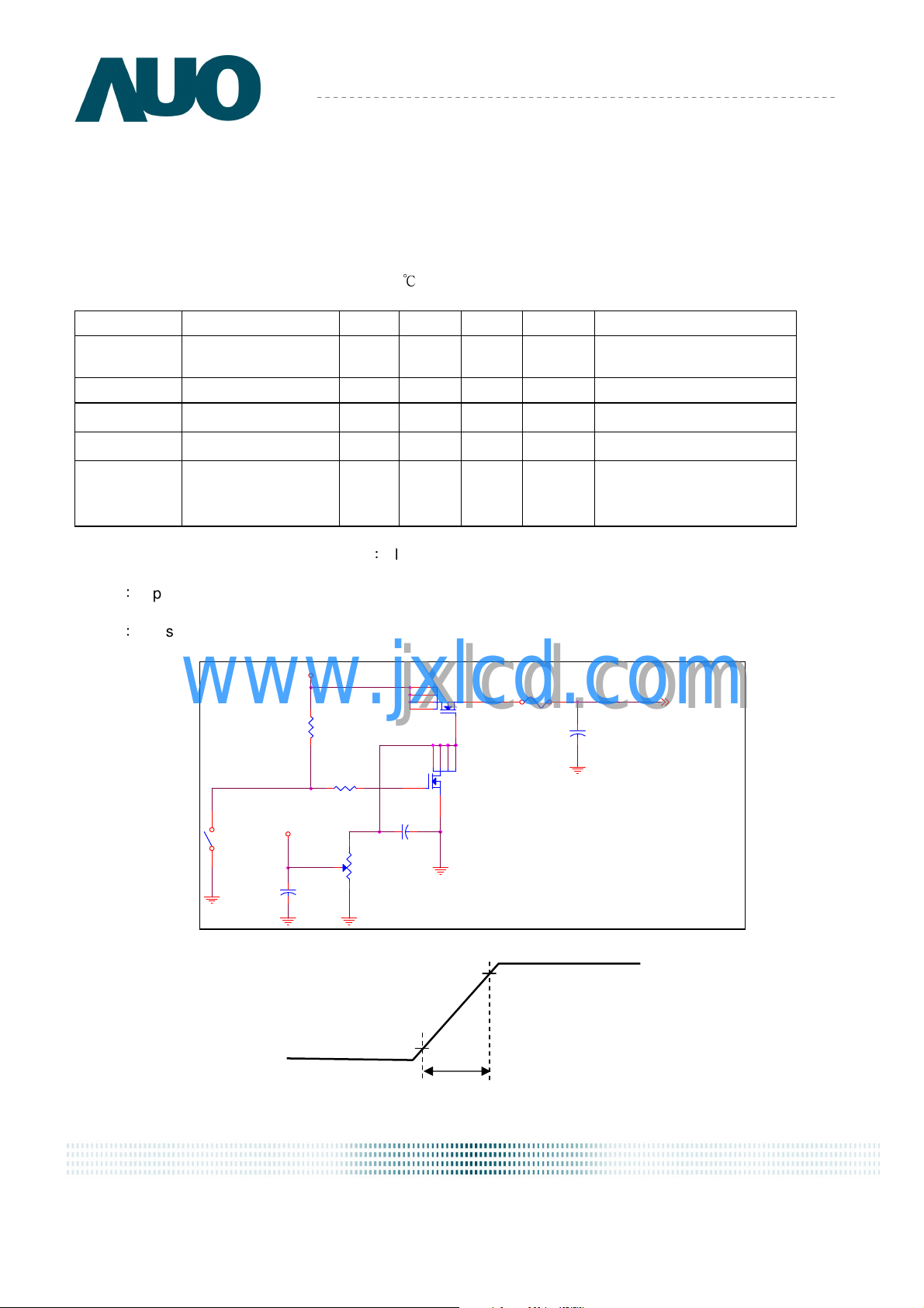
3. Functional Block Diagram
The following diagram shows the functional block of the 14.1 inches wide Color TFT/LCD 30 Pin
One ch / connector Module:
( 4 pairs LVDS )
AU OPTRONICS CORPORATION
LCD DRIVE
BOARD
X-Driver
VDD
GND
JAE FI-XB30SL-HF10
www.jxlcd.com
Mating Housing JAE FI-X30H
www.jxlcd.com
LCD
Con trolle r
DC-DC
Conve rter
Ref circuit
Y-Driver
TFT ARRAY/CELL
1280(R/G/B) x 3 x 800
Backlight Unit
HRS FH33-12S-0.5SH(05)
B141EW05 V2 Document Version: 0.5
11 of 35
Page 12
Product Specification
4. Absolute Maximum Ratings
An absolute maximum rating of the module is as following:
4.1 Absolute Ratings of TFT LCD Module
Item Symbol Min Max Unit Conditions
AU OPTRONICS CORPORATION
Logic/LCD Drive Voltage
Vin -0.3 +4.0 [Volt] Note 1,2
4.2 Absolute Ratings of Backlight Unit
Item Symbol Min Typ Unit Conditions
LED Light bar Driving
LED Light bar Driving
V
LED
I
-
LED
25.2 (Row Output)
20 (Row Output)
[Volt] Note 1,2,3
[mA] rms Note 1,3
4.3 Absolute Ratings of Environment
Item Symbol Min Max Unit Conditions
Operating Temperature
Operation Humidity HOP 8 95 [%RH] Note 4
Storage Temperature
Storage Humidity HST
Note 1: At Ta (25℃ )
Note 2:
Note 3: LED specification refer to section 5.2
Note 4: For quality performance, please refer to AUO IIS (Incoming Inspection Standard).
I
=20mA
LED
www.jxlcd.com
www.jxlcd.com
TOP 0 +50 [oC] Note 4
TST -20 +65 [oC] Note 4
5 95
Twb=39°C
[%RH]
Note 4
Operating Range
B141EW05 V2 Document Version: 0.5
Storage Range
12 of 35
Page 13
Product Specification
Voltage
-
90%
10%
5. Electrical characteristics
5.1 TFT LCD Module
5.1.1 Power Specification
Input power specifications are as follows;
The power specification are measured under 25℃ and frame frenquency under 60Hz
AU OPTRONICS CORPORATION
Symble Parameter Min Typ Max Units
VDD Logic/LCD Drive
PDD VDD Power
IDD IDD Current
I
Rush
Inrush Current
VDDrp Allowable
3.0 3.3 3.6 [Volt]
- 1.1 [Watt] Note 1/2
- 350
- -
- -
450
2000 [mA]
100 [mV]
Logic/LCD Drive
Ripple Voltage
Note 1 : Maximum Measurement Condition:Black Pattern
Note 2:Typical Measurement Condition: Mosaic Pattern
Note 3:Measure Condition
+5.0V
www.jxlcd.com
www.jxlcd.com
(High to Low)
Control
Signal
SW1
SW MAG-SPST
1 2
+12.0V
R1
47K
R2
1K
VR1
47K
D6
D5
D2 S
D1
G
C3
0.01uF/25V
Q3
AO6402
D2SD1D5
G
D6
Q3
AO6402
F1
[mA]
p-p
Note 1/2
Note 3
(LCD Module Input)
C1
1uF/16V
Note
VCC
C2
1uF/25V
3.3V
0V
0.5ms
Vin rising time
B141EW05 V2 Document Version: 0.5
13 of 35
Page 14

Product Specification
VSS
5.1.2 Signal Electrical Characteristics
Input signals shall be low or High-impedance state when VDD is off.
It is recommended to refer the specifications of THC63LVDF84A (Thine Electronics Inc.) in
detail.
Signal electrical characteristics are as follows;
AU OPTRONICS CORPORATION
Parameter
Vth
Vtl
Vcm
Note: LVDS Signal Waveform
V
t
Differential Input High
Threshold (Vcm=+1.2V)
Differential Input Low
Threshold (Vcm=+1.2V)
Differential Input
Common Mode Voltage
www.jxlcd.com
www.jxlcd.com
Condition Min Max Unit
Vcm
-
-100
1.125
100
-
1.375
[mV]
[mV]
[V]
B141EW05 V2 Document Version: 0.5
14 of 35
Page 15

Product Specification
Note 1
5.2 Backlight Unit
LED Parameter guideline for LED driving selection (Ref. Remark 1)
AU OPTRONICS CORPORATION
Parameter
LED Forward Voltage VF 2.95 3.15 3.35
LED Forward Current IF 20 30 [mA]
LED Life-Time
Note 1: Calculator value for LED chip specification
Note 2: The LED life-time define as the estimated time to 50% degradation of initial luminous.
Symbol
N/A 10,000
Min Typ Max
- -
Units Condition
[Volt]
Hour
(Ta=25℃)
(Ta=25℃)
(Ta=25℃)
IF=20 mA
Note 2
www.jxlcd.com
www.jxlcd.com
B141EW05 V2 Document Version: 0.5
15 of 35
Page 16

Product Specification
R G B
B
6. Signal Characteristic
6.1 Pixel Format Image
Following figure shows the relationship of the input signals and LCD pixel format.
1
AU OPTRONICS CORPORATION
1280
1st Line
800th Line
R G B B G R
R G B
www.jxlcd.com
www.jxlcd.com
R G B R G B
R G B R G
B141EW05 V2 Document Version: 0.5
16 of 35
Page 17

Product Specification
Data Clock
6.2 The input data format
Signal Name
R5
R4
R3
R2
R1
R0
Description
Red Data 5 (MSB)
Red Data 4
Red Data 3
Red Data 2
Red Data 1
Red Data 0 (LSB)
Red-pixel Data
AU OPTRONICS CORPORATION
Red-pixel Data
Each red pixel's brightness data consists of
these 6 bits pixel data.
G5
G4
G3
G2
G1
G0
B5
B4
B3
B2
B1
B0
RxCLKIN
DE Display Timing This signal is strobed at the falling edge of
VS Vertical Sync The signal is synchronized to RxCLKIN .
HS Horizontal Sync The signal is synchronized to RxCLKIN .
Note: Output signals from any system shall be low or High-impedance state when VDD is off.
Green Data 5 (MSB)
Green Data 4
Green Data 3
www.jxlcd.com
www.jxlcd.com
Green Data 2
Green Data 1
Green Data 0 (LSB)
Green-pixel Data
Blue Data 5 (MSB)
Blue Data 4
Blue Data 3
Blue Data 2
Blue Data 1
Blue Data 0 (LSB)
Blue-pixel Data
Green-pixel Data
Each green pixel's brightness data consists of
these 6 bits pixel data.
Blue-pixel Data
Each blue pixel's brightness data consists of
these 6 bits pixel data.
The signal is used to strobe the pixel data and
DE signals. All pixel data shall be valid at the
falling edge when the DE signal is high.
RxCLKIN. When the signal is high, the pixel
data shall be valid to be displayed.
B141EW05 V2 Document Version: 0.5
17 of 35
Page 18

Product Specification
6.3 Signal Description/Pin Assignment
LVDS is a differential signal technology for LCD interface and high speed data transfer device.
AU OPTRONICS CORPORATION
1
1
2
2
3
3
4
4
5
5
6
6
7
7
8
8
9
9
10
10
11
11
12
12
13
13
FunctionSymbolPIN#
FunctionSymbolPIN#
www.jxlcd.com
www.jxlcd.com
Ground GND
Ground GND
+3.3V Power SupplyVDD
+3.3V Power SupplyVDD
+3.3V Power SupplyVDD
+3.3V Power SupplyVDD
+3.3V EDID PowerVEDID
+3.3V EDID PowerVEDID
No Connection (Reserve for AUO test)NC
No Connection (Reserve for AUO test)NC
EDID Clock InputCLKEDID
EDID Clock InputCLKEDID
EDID Data InputDATAEDID
EDID Data InputDATAEDID
-LVDS differential data input (R0-R5, G0)RxIN0-
-LVDS differential data input (R0-R5, G0)RxIN0-
+LVDS differential data input (R0-R5, G0)RxIN0+
+LVDS differential data input (R0-R5, G0)RxIN0+
Ground GND
Ground GND
-LVDS differential data input(G1-G5, B0-B1)RxIN1-
-LVDS differential data input(G1-G5, B0-B1)RxIN1-
+LVDS differential data input(G1-G5, B0-B1)RxIN1+
+LVDS differential data input(G1-G5, B0-B1)RxIN1+
Ground GND
Ground GND
14
14
15
15
-LVDS differential data input(B2-B5, HS, VS, DE)RxIN2-
-LVDS differential data input(B2-B5, HS, VS, DE)RxIN2-
+LVDS differential data input(B2-B5, HS, VS, DE)RxIN2+
+LVDS differential data input(B2-B5, HS, VS, DE)RxIN2+
B141EW05 V2 Document Version: 0.5
18 of 35
Page 19
Product Specification
16
16
17
17
18
18
19
19
20
20
21
21
22
22
23
23
24
24
25
25
AU OPTRONICS CORPORATION
Ground GND
Ground GND
-LVDS differential clock inputRxCLKIN-
-LVDS differential clock inputRxCLKIN-
+LVDS differential clock inputRxCLKIN+
+LVDS differential clock inputRxCLKIN+
Ground GND
Ground GND
No ConnectionNC
No ConnectionNC
No Connection)NC
No Connection)NC
Ground GND
Ground GND
No ConnectionNC
No ConnectionNC
No ConnectionNC
No ConnectionNC
Ground GND
Ground GND
FunctionSymbolPIN#
FunctionSymbolPIN#
26
26
27
27
28
28
29
29
30
30
www.jxlcd.com
www.jxlcd.com
No Connection NC
No Connection NC
No Connection NC
No Connection NC
Ground GND
Ground GND
No ConnectionNC
No ConnectionNC
No ConnectionNC
No ConnectionNC
B141EW05 V2 Document Version: 0.5
19 of 35
Page 20

GND
NC
Note1: Start from right side
Product Specification
AU OPTRONICS CORPORATION
30 1
www.jxlcd.com
www.jxlcd.com
Note2: Input signals shall be low or High-impedance state when VDD is off.
B141EW05 V2 Document Version: 0.5
20 of 35
Page 21

Product Specification
12
internal circuit of LVDS inputs are as following.
The module uses a 100ohm resistor between positive and negative data lines of each receiver input
Signal Input
Pin No .
8
RxIN0-
9
RxIN0+
11
RxIN1-
RxIN1+
14
RxIN2-
15
RxIN2+
AU OPTRONICS CORPORATION
LVDS Receiver
R
R
R
17
18
RxCLK IN-
RxCLKIN+
R
www.jxlcd.com
www.jxlcd.com
B141EW05 V2 Document Version: 0.5
21 of 35
Page 22

Product Specification
6.4 Interface Timing
6.4.1 Timing Characteristics
Basically, interface timings should match the 1280x800 /60Hz manufacturing guide line timing.
Parameter Symbol Min. Typ. Max. Unit
Frame Rate - - 60 - Hz
AU OPTRONICS CORPORATION
Clock frequency 1/ T
Vertical
Section
Horizontal
Section
Note : DE mode only
www.jxlcd.com
www.jxlcd.com
Period TV 808 823 1023
Active TVD 800 800 800
Blanking TVB 8 23 223
Period TH 1310 1438 2047
Active THD 1280 1280 1280
Blanking THB 30 158 767
- 71.1 - MHz
Clock
T
T
Clock
Line
B141EW05 V2 Document Version: 0.5
22 of 35
Page 23
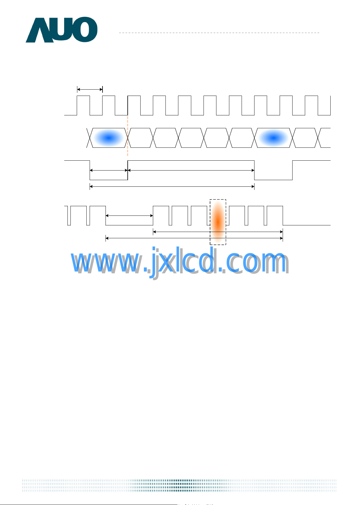
6.4.2 Timing diagram
T
CLOCK
DOTCLK
Input
Data
DE
DE
www.jxlcd.com
www.jxlcd.com
Invaild
Data
Product Specification
AU OPTRONICS CORPORATION
Input Timing Definition ( DE Mode)
Pixel
1
T
HB
T
VB
Pixel
2
T
Pixel
3
T
HD
H
T
V
Pixel
N-1
T
VD
Pixel
N
Invaild
Data
Pixel
1
B141EW05 V2 Document Version: 0.5
23 of 35
Page 24

Product Specification
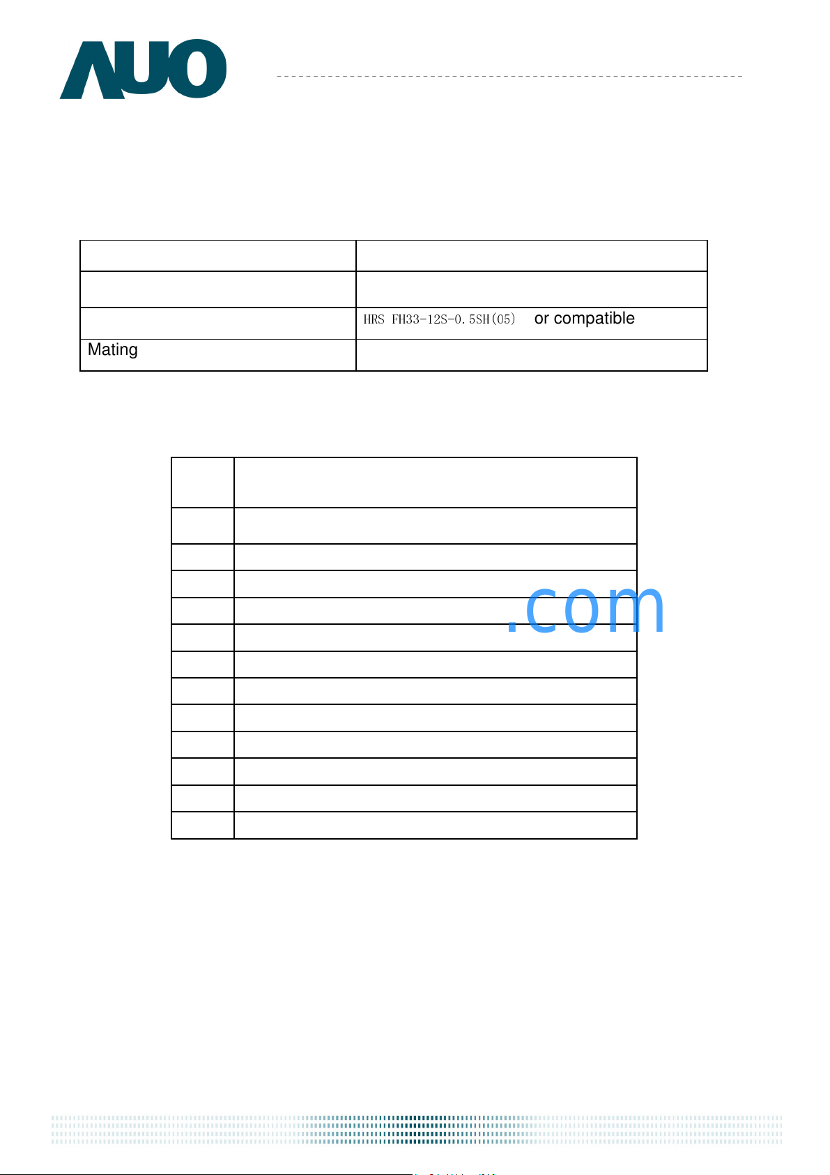
7. Connector Description
Physical interface is described as for the connector on module.
These connectors are capable of accommodating the following signals and will be following
components.
7.1 TFT LCD Module
Connector Name / Designation For Signal Connector
AU OPTRONICS CORPORATION
Manufacturer
Type / Part Number
Mating Housing/Part Number
www.jxlcd.com
www.jxlcd.com
JAE
or compatible
JAE FI-XB30SL-HF10
JAE FI-X30H
or compatible
or compatible
B141EW05 V2 Document Version: 0.5
24 of 35
Page 25
Product Specification
8. LED Driving Specification
8.1 Connector Description
Connector Name / Designation For Signal Connector
AU OPTRONICS CORPORATION
Manufacturer
Type / Part Number
Mating Housing/Part Number compatible
HRS
HRS FH33-12S-0.5SH(05)
8.2 Pin Assignment
www.jxlcd.com
www.jxlcd.com
LCD channel 1 cathode 1
LCD channel 1 cathode 1
LCD channel 2 cathode 2
LCD channel 2 cathode 2
LCD channel 3 cathode 3
LCD channel 3 cathode 3
LCD channel 4 cathode 4
LCD channel 4 cathode 4
LCD channel 5 cathode 5
LCD channel 5 cathode 5
LCD channel 6 cathode ( May be NC if channel<6)6
LCD channel 6 cathode ( May be NC if channel<6)6
or compatible
Signal Name
Signal Name
DescriptionPIN#
DescriptionPIN#
or compatible
LCD channel 7 cathode ( May be NC if channel<7)7
LCD channel 7 cathode ( May be NC if channel<7)7
LCD channel 8 cathode ( May be NC if channel<8)8
LCD channel 8 cathode ( May be NC if channel<8)8
NC9
NC9
LED power bus ( LED Anode)10
LED power bus ( LED Anode)10
LED power bus ( LED Anode)11
LED power bus ( LED Anode)11
LED power bus ( LED Anode)12
LED power bus ( LED Anode)12
B141EW05 V2 Document Version: 0.5
25 of 35
Page 26

Product Specification
9. Vibration and Shock Test
9.1 Vibration Test
Test Spec:
Test method: Non-Operation
Acceleration: 1.5 G , Half sine pulse
Frequency: 10 - 500Hz Sine wave
Sweep: 30 Minutes each Axis (X, Y, Z)
9.2 Shock Test Spec:
AU OPTRONICS CORPORATION
Test Spec:
Test method: Non-Operation
Acceleration: 240 G , Half sine pulse
Active time: 2 ms
Pulse: X,Y,Z .one time for each side
www.jxlcd.com
www.jxlcd.com
B141EW05 V2 Document Version: 0.5
26 of 35
Page 27

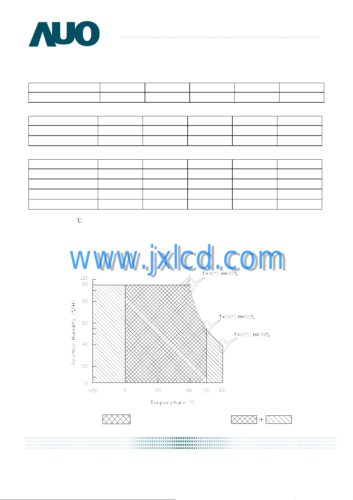
10. Reliability
Items
Temperature
Humidity Bias
High Temperature
Operation
Low Temperature
Operation
High Temperature
Storage
Low Temperature
Storage
Thermal Shock
Test
Product Specification
AU OPTRONICS CORPORATION
Required Condition Note
Ta= 40
Ta= 50
Ta= 0
Ta= 60
Ta= -20
Ta=-20
℃℃℃℃
, 90%RH, 300h
℃℃℃℃
, Dry, 300h
℃℃℃℃
, 300h
℃℃℃℃
, 300h
℃℃℃℃
, 300h
℃℃℃℃
to 60
℃℃℃℃
, Duration at 30 min, 100 cycles
ESD
Note1:
Remark:
According to EN 61000-4-2 , ESD class B: Some performance degradation allowed. No data lost
. Self-recoverable. No hardware failures.
MTBF (Excluding the LED): 30,000 hours with a confidence level 90%
www.jxlcd.com
www.jxlcd.com
Contact : ±8 KV
Air : ±15 KV
Note 1
B141EW05 V2 Document Version: 0.5
27 of 35
Page 28
Product Specification
11. Mechanical Characteristics
11.1 LCM Outline Dimension
AU OPTRONICS CORPORATION
www.jxlcd.com
www.jxlcd.com
B141EW05 V2 Document Version: 0.5
28 of 35
Page 29
Product Specification
AU OPTRONICS CORPORATION
www.jxlcd.com
www.jxlcd.com
B141EW05 V2 Document Version: 0.5
29 of 35
Page 30
Product Specification
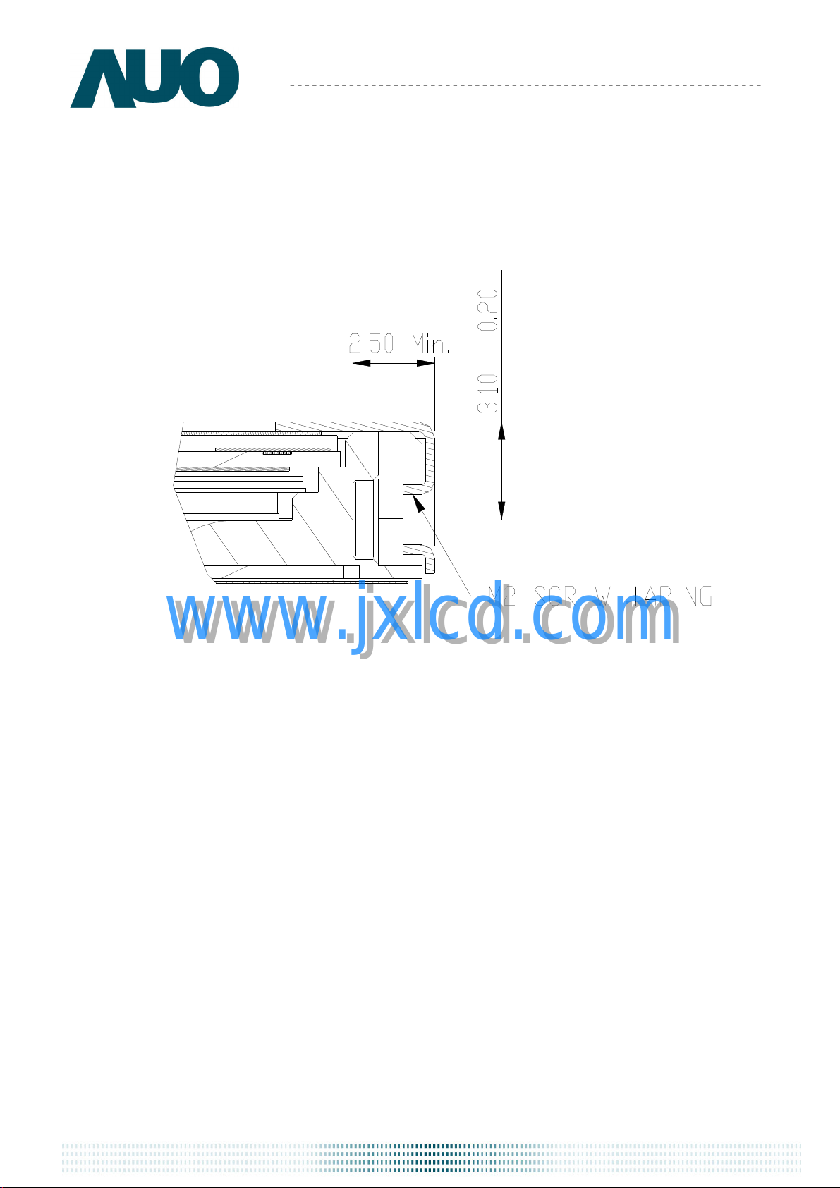
11.2 Screw Hole Depth and Center Position
Screw hole minimum depth, from side surface = 2.5 mm (See drawing)
Screw hole center location, from front surface = 3.1 ± 0.2mm (See drawing)
AU OPTRONICS CORPORATION
Screw Torque: Maximum 2.5 kgf-cm
www.jxlcd.com
www.jxlcd.com
B141EW05 V2 Document Version: 0.5
30 of 35
Page 31

Product Specification
AU OPTRONICS CORPORATION
12. Shipping and Package
12.1 Shipping Label Format
* XXXXXXXXXXXX-XXXXXX
* XXXXXXXXXXXX-XXXXXX
www.jxlcd.com
www.jxlcd.com
Manufactured 0938
Manufactured 0938
Model No: B141EW05
Model No: B141EW05
AU Optronics
AU Optronics
MADE IN CHINA (S1)
MADE IN CHINA (S1)
H/W: 1A F/W:1
H/W: 1A F/W:1
V.2
V.2
1AXXG
1AXXG
C US
C US
C US
C US
C USC US
C USC US
xxxxxxx
xxxxxxx
xxxxxxx
xxxxxxx
xxxxxxxxxxxxxx
xxxxxxxxxxxxxx
Pb
Pb
RoHS
RoHS
B141EW05 V2 Document Version: 0.5
31 of 35
Page 32

Product Specification
12.2 Carton package
The outside dimension of carton is 455 (L)mm x 380 (W)mm x 355 (H)mm
AU OPTRONICS CORPORATION
www.jxlcd.com
www.jxlcd.com
11.3 Shipping package of palletizing sequence
B141EW05 V2 Document Version: 0.5
32 of 35
Page 33

Product Specification
13. Appendix: EDID description
Addres s FU NCT IO N V alue Valu e V alue Note
HE X HE X B IN DE C
00
01
02
03
04
05
06
07
08
09
0A
0B
0C
0D
0E
0F
10
11
12
13
14
15
16
17
18
19
1A
1B
1C
1D
1E
1F
20
21
22
23
24
25
26
27
28
29
2A
2B
2C
2D
2E
2F
30
31
32
33
34
Vide o in put d ef.
Fe ature sup port
Re d/green low b its
Blue/w hite lo w bits
www.jxlcd.com
www.jxlcd.com
EISA M an uf. Co de LS B 06 0 000 0110 6
Co m pressed A SCII AF 1 010 11 11 175
Product Code
hex, LSB first
32 -bit se r # 00 00 00 000 0 0
W eek o f m a nufacture 01 000 00001 1
Year of m anu fa cture 12 00010 010 1 8
ED ID S truc ture Ver. 0 1 00000 001 1
ED ID revision # 03 00 000 01 1 3
Max H imag e size
Max V imag e size
Disp la y Gam m a
(no D PM S , Ac tiv e OF F, RGB , tmg B lk #1)
Red x
Re d y/ high ER 8 bits 58 01 01 100 0 88
Establish ed tim in g 1 00 0 000 0000 0
Establish ed tim in g 2 00 0 000 0000 0
Establish ed tim in g 3 00 0 000 0000 0
Sta nda rd timing #1 01 000 00001 1
Sta nda rd timing #2 01 000 00001 1
Sta nda rd timing #3 01 000 00001 1
Sta nda rd timing #4 01 000 00001 1
Sta nda rd timing #5 01 000 00001 1
Sta nda rd timing #6 01 000 00001 1
Sta nda rd timing #7 01 000 00001 1
Sta nda rd timing #8 01 000 00001 1
AU OPTRONICS CORPORATION
Header 00 000 00000 0
FF 1 111 1111 255
FF 1 111 1111 255
FF 1 111 1111 255
FF 1 111 1111 255
FF 1 111 1111 255
FF 1 111 1111 255
00 000 00000 0
44 010 00100 68
52 010 10010 82
00 000 00000 0
00 000 00000 0
00 000 00000 0
(dig ita l I/P , n on -T MD S , C RGB )
(ro un de d to cm )
(ro un de d to cm )
(=(gamm a*100)-100)
(Lower 2:2:2:2 bits )
(Low e r 2:2:2: 2 bits )
(Upper 8 bits)
Gree n x 57 010 10111 87
Gree n y 93 100 10011 147
Blue x 28 001 01000 40
Blue y 1E 000 11110 3 0
W h ite x 50 01010000 8 0
W h ite y 54 0 10 101 00 84
80 100 00000 128
1E 0 001 1110 30
13 000 10011 19
78 011 11000 120
0A 0 000 1010 10
26 001 00110 38
75 011 10101 117
96 100 10110 150
01 000 00001 1
01 000 00001 1
01 000 00001 1
01 000 00001 1
01 000 00001 1
01 000 00001 1
01 000 00001 1
B141EW05 V2 Document Version: 0.5
33 of 35
Page 34

Product Specification
35
36
Pix el Clock /100 00 LSB
37
Pix el Clock /100 00 US B
38
Ho rz active Lower 8bits
39
Ho rz blanking
3A
Ho rzAct:HorzBln k Upp er 4:4 bits
3B
3C
3D
3E
3F
40
41
42
43
44
45
46
47
48
49
4A
4B
4C
4D
4E
4F
50
51
52
53
54
55
56
57
58
59
5A
5B
5C
5D
5E
5F
60
61
62
63
64
65
66
67
68
69
6A
6B
6C
6D
6E
6F
Vertical A ctive Lo w er 8bits
Vertical B lank ing Lower 8bits
Vert Ac t : Vertical Blanking
HorzSyn c. O ffset
HorzSyn c.W idth
VertSync.Offset : Ve rtSync.W idth
Ho rz&V ert Syn c Offset/W idth Upper 2bits
Horiz on ta l Image Size
Ve rtica l Image Size
Horiz on ta l & V ertic al Ima ge S ize
Horiz on ta l B order
Vertical B order
Sig na l
(non-intr, no rm , n o ste ro, s ep sy nc , n eg po l)
www.jxlcd.com
www.jxlcd.com
Lo w er 8bits
Lo w er 8bit s
(zero for internal LCD)
(zero f or internal LC D)
De taile d tim ing/m on itor 00 00 00000 0 0
desc rip to r #2 00 0 00000 00 0
De taile d tim ing/m on itor 00 00 00000 0 0
desc rip to r #3 00 0 00000 00 0
Manu facture 4 1 01000 00 1 65 A
Manu facture 5 5 01010 10 1 85 U
Manu facture 4F 010011 11 79 O
De taile d tim ing/m on itor 00 00 00000 0 0
desc rip to r #4 00 0 00000 00 0
AU OPTRONICS CORPORATION
(upper 4:4 bit)
Lo w er 8bits
(upper 4:4 bits)
01 0 00 00001 1
C6 110001 10 198
1B 00 01101 1 2 7
00 0 00 00000 0
9E 10 01111 0 158
50 0 10 10000 80
20 0 01 00000 32
17 0 00 10111 23
30 0 01 10000 48
30 0 01 10000 48
20 0 01 00000 32
36 0 01 10110 54
00 0 00 00000 0
2F 001 01 111 47
BD 101 11 101 189
10 0 00 10000 16
00 0 00 00000 0
00 0 00 00000 0
18 0 00 11000 24
00 0 00 00000 0
0F 000 01 111 15
00 0 00 00000 0
00 0 00 00000 0
00 0 00 00000 0
00 0 00 00000 0
00 0 00 00000 0
00 0 00 00000 0
00 0 00 00000 0
00 0 00 00000 0
00 0 00 00000 0
00 0 00 00000 0
00 0 00 00000 0
00 0 00 00000 0
00 0 00 00000 0
20 0 01 00000 32
00 0 00 00000 0
FE 111111 10 254
00 0 00 00000 0
0A 00 00101 0 1 0
20 0 01 00000 32
20 0 01 00000 32
20 0 01 00000 32
20 0 01 00000 32
20 0 01 00000 32
20 0 01 00000 32
20 0 01 00000 32
20 0 01 00000 32
20 0 01 00000 32
00 0 00 00000 0
FE 111111 10 254
B141EW05 V2 Document Version: 0.5
34 of 35
Page 35

Product Specification
SUM to HEX
70
71 Manufacture P/N 42 01000010 66 B
72 Manufacture P/N 31 00110001 49 1
73
74
75
76
77
78
79 Manufacture P/N 20 00100000 32
7A Manufacture P/N 56 01010110 86 V
7B
7C
7D
7E
7F
Manufacture P/N 34 00110100 52 4
Manufacture P/N 31 00110001 49 1
Manufacture P/N 45 01000101 69 E
Manufacture P/N 57 01010111 87 W
Manufacture P/N 30 00110000 48 0
Manufacture P/N 35 00110101 53 5
Manufacture P/N 32 00110010 50 2
Extension Flag 00 00000000 0
Checksum 4F 01001111 79
AU OPTRONICS CORPORATION
00 00000000 0
20 00100000 32
0A 00001010 10
SUM 5888
1700
www.jxlcd.com
www.jxlcd.com
B141EW05 V2 Document Version: 0.5
35 of 35
 Loading...