

Page 1
AUO
Display Specification for B133EW07 V0
13.3” Wide (1280x800) TFT-LCD
LED Backlight with High Color Gamut
| Size: A | METRIC | Scale: NONE | Page 1 of 54
Title: Spec, Elec., Dspl., AUO, 13.3” TFT-LCD, DWG Number: 069-3542 Rev.01
www.jxlcd.com
www.jxlcd.com
Page 2

Revision History
DATE REV # Section # CHANGE DESCRIPTION
www.jxlcd.com
www.jxlcd.com
N
. | Size: A | METRIC | Scale: NONE | Page 2 of 55
Title: Spec, Elec., Dspl., AUO, 13.3” TFT-LCD DWG Number: 069-3542 Rev.01
Page 3
Table of Content
Revision History 2
1. General Description 6
2. ORDER OF PRECEDENCE OF DOCUMENTATION AUTHORITY 7
2.1. The Purchase Order 7
2.2. This Specification 7
2.3. Reference Documents 7
3. PHYSICAL DESCRIPTION 8
4. MECHANICAL REQUIREMENTS 9
5. ELECTRICAL REQUIREMENTS 11
5.1. Block Diagram 11
5.2. Display PCB Schematics 12
5.3. Display PCB Layout 13
5.4. Display Subsystem (PCB & TFT Panel) 13
5.4.1. Pin-Out (Single Channel LVDS Interface) 13
5.4.2. Connector Diagram 14
5.4.3. Color Input Data Reference 15
5.4.4. EDID Interface (Per Vesa EDID 1.x standard requirements) 17
5.4.5. Electrical Ratings 20
5.4.6. Signal Timing 22
5.4.6.1. Signal Impedance 22
5.4.6.2. Timing Data 22
5.4.6.3. Video Timing Diagram 23
5.4.7. Power Measurements (W/O backlight) 25
5.4.8. Power on-off sequence 26
5.4.9. Vcc Dip Condition 26
5.5. Near-Field Noise 27
5.6. Backlight Subsystem 27
6. OPTICAL REQUIREMENTS 30
6.1. Optical Specifications 30
6.2. Measuring Conditions 31
N
. | Size: A | METRIC | Scale: NONE | Page 3 of 55
Title: Spec, Elec., Dspl., AUO, 13.3” TFT-LCD DWG Number: 069-3542 Rev.01
www.jxlcd.com
www.jxlcd.com
Page 4
6.3. Definition 33
6.3.1. Center Point Luminance 33
6.3.2. Average Luminance 33
6.3.3. Luminance Uniformity 33
6.3.3.1. Global Luminance Uniformity: 33
6.3.3.2. Worst Neighbor Luminance Uniformity (The 4 points that are closest to the test point)
34
6.3.4. Contrast Ratio 34
6.3.5. White Color Uniformity 34
6.3.5.1. Panel to Panel White Color Uniformity 34
6.3.5.2. Max Color Difference with respect to the center within a panel 35
6.3.5.3. Max Color Difference between any two points within the panel 35
6.3.5.4. Max Color Difference between two neighbors 35
6.3.6. RGB Color Chromaticity 35
6.3.7. Viewing Angle 35
6.3.8. Gray Scale Inversion 36
6.3.9. Response Time 36
6.3.9.1. On and Off Response Time 36
6.3.9.2. Gray to Gray Response Time 36
6.3.10. Gray Scale Linearity or Gamma Value 37
6.3.11. Flicker 37
6.3.12. Cross-talk 38
6.4. Hot Spot Specifications: 38
7. ENVIRONMENTAL 40
7.1. Shock and Vibration 40
7.2. Temperature and Humidity 41
7.2.1. General Performance Requirements 41
7.2.2. Non-operational Testing 42
7.2.2.1. Low Temperature 42
7.2.2.2. High Temperature 42
7.2.2.3. High Temperature and High Humidity 42
7.2.2.4. Thermal Shock 42
7.2.3. Operational Testing 42
www.jxlcd.com
www.jxlcd.com
N
. | Size: A | METRIC | Scale: NONE | Page 4 of 55
Title: Spec, Elec., Dspl., AUO, 13.3” TFT-LCD DWG Number: 069-3542 Rev.01
Page 5
7.2.3.1. Low Temperature 42
7.2.3.2. High Temperature 42
7.2.3.3. High Temperature and High Humidity 42
7.2.3.4. Four Corner Test (72 hrs – operating) 42
7.3. Altitude 43
8. RELIABILITY 43
8.1. Resistance to Normal Abuse 43
8.1.1. Torsion Test 43
8.1.2. Test Conditions: 43
8.1.3. Test Set-up 44
8.1.4. Static Load Deflection and Breakage 44
8.2. Electrostatic Discharge (ESD) 44
8.3. MTBF 44
8.4. LCD Glass Strength 45
9. COSMETIC REQUIREMENTS 50
10. REGULATORY 51
10.1. Product Safety (Environmental, Ergonomics, Safety and Health) 51
10.2. RoHS Compliance and other Substance Regulations 51
10.3 Halogen Free 51
10.3. Environmental Markings and Recycling 51
10.4. Product Safety 52
10.5. Ergonomics 52
10.6. Electromagnetic Compatibility (EMC) 52
11 FACTORY/SERVICE REQUIREMENTS 54
12 REFERENCE DOCUMENTS 55
www.jxlcd.com
www.jxlcd.com
N
. | Size: A | METRIC | Scale: NONE | Page 5 of 55
Title: Spec, Elec., Dspl., AUO, 13.3” TFT-LCD DWG Number: 069-3542 Rev.01
Page 6
1. General Description
This document establishes the requirements for the display device for the B133EW07 V0
Category Parameter Specification
General
Electrical
Optical
Manufacturer AUO
Mfg. P/N B133EW07 V0
LCD TYPE Normally-White, Transmissive TN TFT-LCD
Diagonal 13.282” (33.74cm)
Pixel Format 1280 (RGB stripe, H) x 800 (V)
Pixel Pitch 0.2235(V) x 3x0.0745(H) mm
Color Depth 18-bits (6R, 6G, 6B), 262144 colors
Pooling requirement Rigid Post Spacer with strong pooling resistance
Packaging Protective film on front polarizer. Displays packaged
and air-tight sealed in anti-static bags.
Interface 3.3V single-channel LVDS
Power Consumption 4.36 W @ Black (typical, the logic plus the backlight
@94% duty cycle @23mA, 3.3V forward bias voltage)
Luminance 275 nits @ 94% duty cycle @23 mA (typical center)
White LED Backlight 6 strings, 9 LED per string. Nichia NNSW208
Hot Spots No visible hot spot at any angle
Viewing Direction 6:00 for worst dark inversion (pcb driver on the bottom)
Mechanical
N
. | Size: A | METRIC | Scale: NONE | Page 6 of 55
Title: Spec, Elec., Dspl., AUO, 13.3” TFT-LCD DWG Number: 069-3542 Rev.01
Contrast 500 typical
www.jxlcd.com
www.jxlcd.com
Top Polarizer Glossy Surface, 3H Hard Coating, LT4/ARC7 AR
coating
Diffuser Sheet Tsujiden D153GS (top) & Tsujiden D120 (Bottom)
BEF Sheet 2 X BEF2-G2 MR (Halogen free)
Reflector E6SR or equivalent (sulfur free)
LGP PMMA
Active Area 286.08 mm (H) x 178.80 mm (V)
Page 7

Minimum Viewing Area 288.08 mm (H) x 180.80 mm (V)
Environmental
Pre-Aging
2. ORDER OF PRECEDENCE OF DOCUMENTATION AUTHORITY
In the case of any conflict in any specification related to these parts, this order of precedence of
authority shall apply:
2.1. The Purchase Order
2.2. This Specification
2.3. Reference Documents
Module Outline Size 297.150 mm (H) x 192.150 mm (V)
Connector IPEX 20474-030E-12
Mating Connector IPEX 20472-030T-10
Weight 300 grams typical
Operating Temperature 0°C ~ +50°C
Storage Temperature -25°C ~ +65°C
Before shipment Minimum 2 hours at 50°C, panel on
www.jxlcd.com
www.jxlcd.com
N
. | Size: A | METRIC | Scale: NONE | Page 7 of 55
Title: Spec, Elec., Dspl., AUO, 13.3” TFT-LCD DWG Number: 069-3542 Rev.01
Page 8
:
3. PHYSICAL DESCRIPTION
3.1. Display Mode
Normally White, Transmissive, Twisted Nematic Liquid Crystal Displays
3.2. Pixel Configuration
RGB Vertical Stripe
3.3. Pixel Pitch
0.2235 mm x 0.2235 mm
3.4. Resolution
1280 (RGB stripe, H) x 800 (V)
3.5. Aperture Ratio
Minimum > 50%
3.6. Optimum Viewing Cone
6 o’clock worst dark inversion direction (PCB on the bottom)
3.7. Interface & Driving Scheme
3.3V single-channel LVDS (Flat Link) interface, requiring Hsync and Vsync
signals, along with DE (Data Enable) mode, 2-dot inversion
3.8. Front Surface Treatment
Low-reflection gloss surface, ~1% Reflectance, ≥3H hardness (Sumitomo LT4, or
Nitto Denko ARC7)
3.9 Environmental Requirements:
Any homogeneous component must meet Halogen-Free Specification, 069-1857.
www.jxlcd.com
www.jxlcd.com
N
. | Size: A | METRIC | Scale: NONE | Page 8 of 55
Title: Spec, Elec., Dspl., AUO, 13.3” TFT-LCD DWG Number: 069-3542 Rev.01
刪除
刪除
刪除刪除
Page 9
4. MECHANICAL REQUIREMENTS
4.1. Dimensions and Tolerances
The LCD module outline is described in the following table.
Dimension Min Typ Max Unit
Horizontal (H) 296.85 297.15 297.45 mm
Vertical (V) 191.85 192.15 192.45 mm
Depth (D) 3.08 3.38 3.68 mm
4.2. Weight
300 g (typical), 310 g (max)
4.3. Stack-up (tentative)
Mechanical Stack-up Part # Thickness /mm
Top Polarizer
(glossy, LT4 or ARC7) Sumika, SRW862APK-LT4
LCD Glass CF 0.5
LCD Glass TFT 0.5
Bottom Polarizer 0.215
Total Design Gap - 0.135
Upper Diffuser Tsujiden D131S 0.095
Upper BEF (Halogen Free) BEF II-GII MR 0.155
Lower BEF (Halogen Free) BEF II-GII MR 0.155
Lower Diffuser Tsujiden D120 0.12
Light Guide PMMA 0.72
White Reflector (Sulfur-free
www.jxlcd.com
www.jxlcd.com
reflector for PMMA
backlight) E6SR 0.188
Rear Bezel SUS 304 0.3
Tape 0.1
Total Typical Thickness w/o PCB 3.38
Maximum Tolerance 0.3
Total Maximum Thickness
PCB Thickness (8 Layer
PCB) 0.8
Maximum Component - 1
side (include Solder) 1.15
N
. | Size: A | METRIC | Scale: NONE | Page 9 of 55
Title: Spec, Elec., Dspl., AUO, 13.3” TFT-LCD DWG Number: 069-3542 Rev.01
(w/o PCB) 3.68
0.215
Page 10
Maximum Component - 2
side (include Solder) 0.2
Total Maximum PCB
Thickness 2.15
4.4. Exposed Areas and Restrictions
The display module shall not have exposed edges or components, which may cause injury
or damage during handling, inspection, assembly, and service. Exposed areas of the display
module (those not protected or shielded by construction) must be insulated and otherwise
protected to eliminate the possibility of electrical shorting or destructive ESD discharges
(per Section 7.2) during handling, inspection, assembly, and service.
www.jxlcd.com
www.jxlcd.com
N
. | Size: A | METRIC | Scale: NONE | Page 10 of 55
Title: Spec, Elec., Dspl., AUO, 13.3” TFT-LCD DWG Number: 069-3542 Rev.01
Page 11
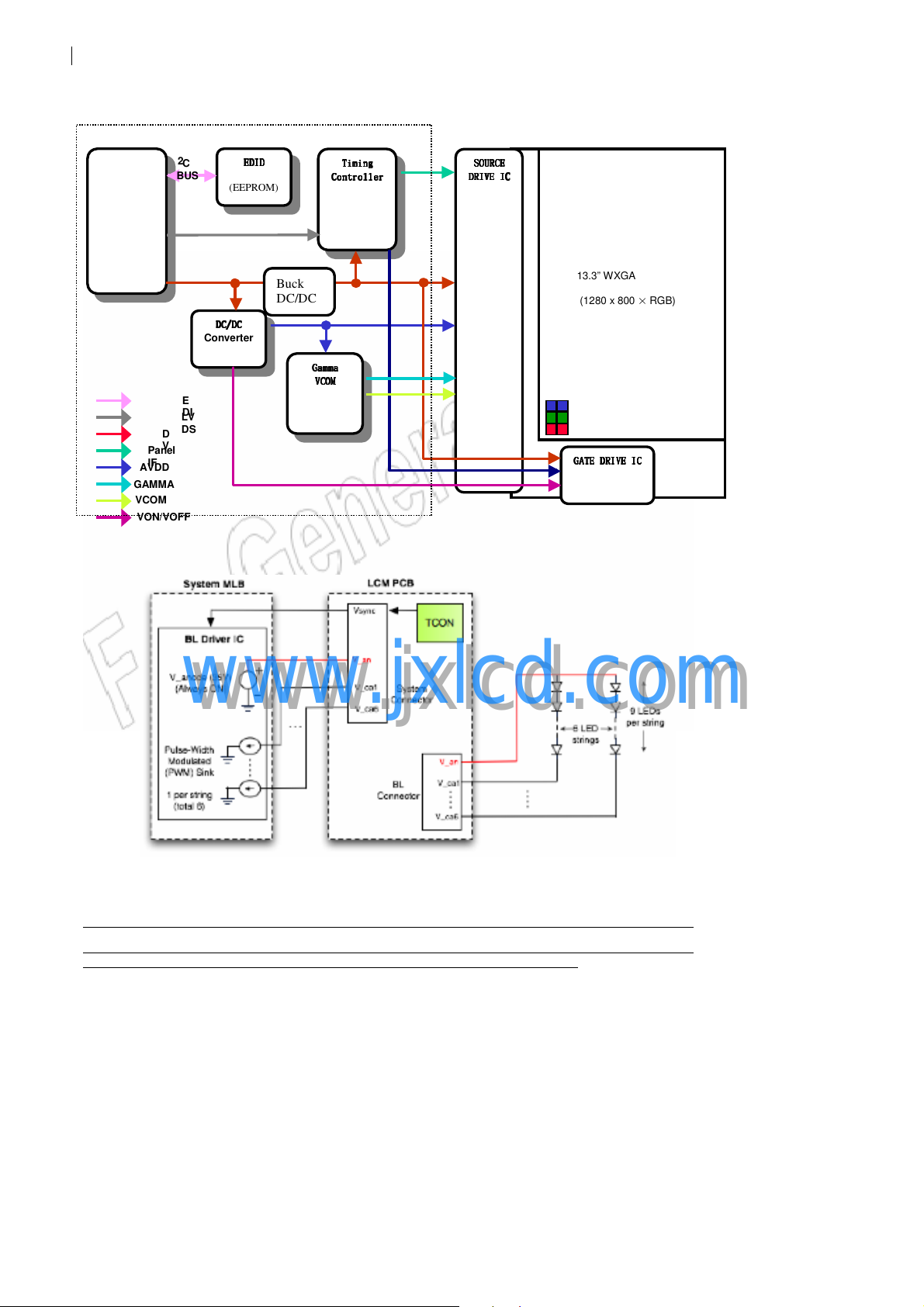
I C
2
Panel
IF
ELECTRICAL REQUIREMENTS
4.5. Block Diagram
Connector
User
BUS
EDID
EDID
EDIDEDID
(EEPROM)
DC/DC
DC/DC
DC/DCDC/DC
Converter
E
DI
LV
DS
D
V
AVDD
GAMMA
VCOM
VON/VOFF
Backlight Driving Architecture
Buck
DC/DC
Generator
Controller
Controller
ControllerController
Gamma
Gamma
GammaGamma
VCOM
VCOM
VCOMVCOM
Timing
Timing
TimingTiming
SOURCE
SOURCE
SOURCESOURCE
DRIVE IC
DRIVE IC
DRIVE ICDRIVE IC
13.3” WXGA
(1280 x 800 × RGB)
GATE DRIVE IC
GATE DRIVE IC
GATE DRIVE ICGATE DRIVE IC
www.jxlcd.com
www.jxlcd.com
N
. | Size: A | METRIC | Scale: NONE | Page 11 of 55
Title: Spec, Elec., Dspl., AUO, 13.3” TFT-LCD DWG Number: 069-3542 Rev.01
Page 12

4.6. Display PCB Schematics
www.jxlcd.com
www.jxlcd.com
N
. | Size: A | METRIC | Scale: NONE | Page 12 of 55
Title: Spec, Elec., Dspl., AUO, 13.3” TFT-LCD DWG Number: 069-3542 Rev.01
Page 13

4.7. Display PCB Layout
Display Subsystem (PCB & TFT Panel)
4.7.1. Pin-Out (Single Channel LVDS Interface)
Connector: IPEX 20474-030E-12 or equivalent (1.0 mm thickness, lock-in type, pin 1
starts from left on the front)
Matching Connector: IPEX 20472-030T-10 or equivalent (micro-coax type)
Interface Chips: (need update according the latest Configuration Sheet), integrated LVDS
and timing controller)
www.jxlcd.com
www.jxlcd.com
Single Channel LVDS Configuration
Pin Symbol Description Micro-coax cable gauge
(AWG)
1 GND Ground 40
2 Vcc Power Supply (+3.3V)
3 V
4 V
N
. | Size: A | METRIC | Scale: NONE | Page 13 of 55
Title: Spec, Elec., Dspl., AUO, 13.3” TFT-LCD DWG Number: 069-3542 Rev.01
Power Supply (+3.3V)
analog
DDC Power +3.3V 40
EDID
36
36
Page 14

5 Vsync Vsync 40
6 Clk
7 DATA
8 Rin0- Differential Data Input 40
9 Rin0+ Differential Data Input 40
10 GND Ground 40
11 Rin1- Differential Data Input 40
12 Rin1+ Differential Data Input 40
13 GND Ground 40
14 Rin2- Differential Data Input 40
15 Rin2+ Differential Data Input 40
16 GND Ground 40
17 Clkin- Differential Clock Input 40
18 Clkin+ Differential Clock Input 40
19 GND Ground 40
20 NC NC 40
21 Vdc(1 &2) LED Annold (Positive) 40
22 Vdc(3&4) LED Annold (Positive) 40
23 NC NC 40
24 Vdc1 LED Cathode (Negative) 40
25 Vdc2 LED Cathode (Negative) 40
26 Vdc3 LED Cathode (Negative) 40
27 Vdc4 LED Cathode (Negative) 40
28 Vdc5 LED Cathode (Negative) 40
29 Vdc6 LED Cathode (Negative) 40
30 NC NC 40
DDC Clock 40
EDID
DDC Data 40
EDID
www.jxlcd.com
www.jxlcd.com
4.7.2. Connector Diagram
N
. | Size: A | METRIC | Scale: NONE | Page 14 of 55
Title: Spec, Elec., Dspl., AUO, 13.3” TFT-LCD DWG Number: 069-3542 Rev.01
PIN #1
PIN #30
格格格格式化
式化::::
式化式化
格格格格式化
式化::::
式化式化
項目符號及編號
項目符號及編號
Page 15

4.7.3. Color Input Data Reference
The brightness of each primary color (red, green and blue) is based on the 6-bit gray
scale data input for the color. The higher the binary input, the brighter the color. The
table below provides a reference for color versus data input.
COLOR DATA REFERENCE
Input Color Data
Color Red
MSB LSB
R5 R4 R3 R2 R1 R0 G5 G4 G3 G2 G1 G0 B5 B4 B3 B2 B1 B0
Basic
Colors
Red
Green
Black
Red(63)
Green(63)
Blue(63)
Cyan
Magenta
Yellow
White
Red(00) Dark
Red(01)
Red(02)
Red(61)
www.jxlcd.com
Red(62)
www.jxlcd.com
Red(63) Bright
Green(00)Dark
Green(01)
Green(02)
Green(61)
Green(62)
Green(63)Bright
0
0
0
0
0
0
0
1
1
1
1
1
1
0
0
0
0
0
0
0
1
0
0
0
0
0
0
0
0
0
0
0
0
0
1
1
1
1
1
1
1
0
1
1
1
1
1
1
1
1
1
1
1
1
1
1
0
0
0
0
0
0
0
0
0
0
0
0
1
0
0
0
0
0
1
0
0
:
:
:
:
:
:
:
1
1
1
1
0
1
0
1
1
1
1
1
0
0
1
1
1
1
1
1
0
0
0
0
0
0
0
0
0
0
0
0
0
0
0
0
0
0
0
0
0
0
:
:
:
:
:
:
:
0
0
0
0
0
0
1
0
0
0
0
0
0
1
0
0
0
0
0
0
1
Green
MSB LSB
0
0
0
0
0
0
0
0
1
1
1
1
0
0
0
0
1
1
1
1
0
0
0
0
1
1
1
1
1
1
1
1
0
0
0
0
0
0
0
0
0
0
0
0
:
:
:
:
0
0
0
0
0
0
0
0
0
0
0
0
0
0
0
0
0
0
0
0
0
0
0
1
:
:
:
:
1
1
1
0
1
1
1
1
1
1
1
1
MSB LSB
0
0
0
0
1
0
0
1
1
1
0
1
1
0
1
1
0
0
0
0
0
0
:
:
0
0
0
0
0
0
0
0
1
0
0
0
:
:
1
0
0
0
1
0
0
0
0
1
1
1
0
1
0
0
0
:
0
0
0
0
0
0
:
0
0
0
Blue
0
0
0
1
1
1
0
1
0
0
0
:
0
0
0
0
0
0
:
0
0
0
0
0
0
0
0
0
0
0
0
1
1
1
1
1
1
1
1
1
0
0
0
1
1
1
0
0
0
0
0
0
0
0
0
:
:
:
0
0
0
0
0
0
0
0
0
0
0
0
0
0
0
0
0
0
:
:
:
0
0
0
0
0
0
0
0
0
N
. | Size: A | METRIC | Scale: NONE | Page 15 of 55
Title: Spec, Elec., Dspl., AUO, 13.3” TFT-LCD DWG Number: 069-3542 Rev.01
Page 16
BRG
R G BRG
B R G B R G
B
L
799
Blue(00) Dark
Blue(01)
Blue(02)
Blue
Blue(61)
Blue(62)
Blue(63) Bright
0
0
0
0
0
0
0
0
0
0
0
0
0
0
0
0
0
0
:
:
:
:
:
:
0
0
0
0
0
0
0
0
0
0
0
0
0
0
0
0
0
0
Pixel Format on the Display
0
0
0
0
0
0
0
0
0
0
0
0
0
0
0
0
0
0
0
0
0
0
0
1
0
0
0
0
0
0
0
0
0
0
1
0
:
:
:
:
:
:
:
:
:
:
:
:
0
0
0
0
0
0
1
1
1
1
0
1
0
0
0
0
0
0
1
1
1
1
1
0
0
0
0
0
0
0
1
1
1
1
1
1
in e 0
0
R G
B
R G B R G B
1279
Scan Direction
Flex Bonding Edge
www.jxlcd.com
www.jxlcd.com
格格格格式化
式化::::
式化式化
項目符號及編號
N
. | Size: A | METRIC | Scale: NONE | Page 16 of 55
Title: Spec, Elec., Dspl., AUO, 13.3” TFT-LCD DWG Number: 069-3542 Rev.01
Page 17
4.7.4. EDID Interface (Per Vesa EDID 1.x standard requirements)
Release
Address
HEX
00
01
02
03
04
05
06
07
08
09
0A
0B
0C
0D
0E
0F
10
11
12
13
14
15
16
17
18
19
1A
1B
1C
1D
1E
1F
20
21
N
. | Size: A | METRIC | Scale: NONE | Page 17 of 55
Title: Spec, Elec., Dspl., AUO, 13.3” TFT-LCD DWG Number: 069-3542 Rev.01
FUNCTION B133EW04
Header
Header
HeaderHeader
00 00000000 0
FF 11111111 255
EISA Manuf. Code
EISA Manuf. Code
EISA Manuf. Code EISA Manuf. Code
LSB
LSB
LSBLSB
Compressed ASCII
Compressed ASCII
Compressed ASCIICompressed ASCII
Product Code
Product Code
Product CodeProduct Code
hex, LSB first
hex, LSB first
hex, LSB firsthex, LSB first
32
32----bit ser #
bit ser #
3232
bit ser #bit ser #
Week of manufacture
Week of manufacture
Week of manufactureWeek of manufacture
Year of manufacture
Year of manufacture
Year of manufactureYear of manufacture
EDID Structure Ver.
EDID Structure Ver.
EDID Structure Ver.EDID Structure Ver.
EDID revision #
EDID revision #
EDID revision #EDID revision #
Video input definition
Video input definition
Video input definitionVideo input definition
Max H image size
Max H image size
Max H image sizeMax H image size
Max V image size
Max V image size
Max V image sizeMax V image size
Display Gamma
Display Gamma
Display GammaDisplay Gamma
www.jxlcd.com
www.jxlcd.com
Feature support
Feature support
Feature supportFeature support
Red/green low bits
Red/green low bits
Red/green low bitsRed/green low bits
Blue/white low bits
Blue/white low bits
Blue/white low bitsBlue/white low bits
Red x/ high bits
Red x/ high bits
Red x/ high bitsRed x/ high bits
Red y
Red y
Red yRed y
Green x
Green x
Green xGreen x
Green y
Green y
Green yGreen y
Blue x
Blue x
Blue xBlue x
Blue y
Blue y
Blue yBlue y
White x
White x
White xWhite x
HEX BIN DEC
FF 11111111 255
FF 11111111 255
FF 11111111 255
FF 11111111 255
FF 11111111 255
00 00000000 0
06 00000110 6
10 00010000 16
A1 10100001 161
9C 10011100 156
01 00000001 1
01 00000001 1
01 00000001 1
01 00000001 1
01 00000001 1
13 00010011 19
01 00000001 1
03 00000011 3
80 10000000 128
1D 00011101 29
12 00010010 18
78 01111000 120
0A 00001010 10
50 01010000 80
85 10000101 133
97 10010111 151
58 01011000 88
50 01010000 80
8E 10001110 142
27 00100111 39
27 00100111 39
50 01010000 80 Wx=0.313
Value Value Note
time 7/11/08 0:00
APP9CA1
APP9CA1
APP9CA1APP9CA1
0 00001(A) 10000(P)
10000(P)
9CA1 ( assigned code)
unused
unused
unusedunused
Week 1
Week 1
Week 1Week 1
19(2009
19(2009----1990=19)
19(200919(2009
1990=19)
1990=19)1990=19)
Digital Input
28.6cm
28.6cm
28.6cm28.6cm
17.9cm
17.9cm
17.9cm17.9cm
Gamma 2.2
Gamma 2.2
Gamma 2.2Gamma 2.2
no DPMS,Active
off,RGB color
Rx=0.640
Ry=0.340
Gx=0.310
Gy=0.610
Bx=0.150
By=0.060
Page 18

White y
White y
22
23
24
25
26
27
28
29
2A
2B
2C
2D
2E
2F
30
31
32
33
34
35
36
37
38
39
3A
3B
3C
3D
3E
3F
40
41
N
White yWhite y
Es
Established timing 1
tablished timing 1
EsEs
tablished timing 1tablished timing 1
Established timing 2
Established timing 2
Established timing 2Established timing 2
Manufacturer's
Manufacturer's
Manufacturer's Manufacturer's
Timing
Timing
TimingTiming
Standard timing #1
Standard timing #1
Standard timing #1Standard timing #1
Standard timing #2
Standard timing #2
Standard timing #2Standard timing #2
St
Standard timing #3
andard timing #3
StSt
andard timing #3andard timing #3
Standard timing #4
Standard timing #4
Standard timing #4Standard timing #4
01 00000001 1
Standard timing #5
Standard timing #5
Standard timing #5Standard timing #5
Standard timing #6
Standard timing #6
Standard timing #6Standard timing #6
01 00000001 1
Standard timin
Standard timing #7
Standard timinStandard timin
Standard timing #8
Standard timing #8
Standard timing #8Standard timing #8
Pixel Clock/10,000
Pixel Clock/10,000
Pixel Clock/10,000 Pixel Clock/10,000
Pixel Clock/10,000
Pixel Clock/10,000
Pixel Clock/10,000 Pixel Clock/10,000
Horiz. Active
pixels(Lower 8 bits) 00 00000000 0
Horiz.Blanking (Lower
Horiz. Active
pixels:Horiz. Blanking
(Upper4:4 bits)
www.jxlcd.com
www.jxlcd.com
Vert. Active
pixels:Vert. Blanking
(Upper4:4 bits)
Vert. Sync. Offset=xx
lines, Sync Width=xx
Horz. Ver. Sync/Width
(upper 2 bits)
g #7
g #7g #7
(LSB)
(LSB)
(LSB)(LSB)
(MSB)
(MSB)
(MSB)(MSB)
8 bits)
20 00100000 32
lines
54 01010100 84 Wy=0.329
00 00000000 0
00 00000000 0
00 00000000 0
01 00000001 1 unused
01 00000001 1
01 00000001 1
01 00000001 1
01 00000001 1
01 00000001 1
01 00000001 1
01 00000001 1
01 00000001 1
01 00000001 1
01 00000001 1
01 00000001 1
01 00000001 1
01 00000001 1
unused
Timing
52 01010010 82
1C 00011100 28
8F 10001111 143
50 01010000 80
2E 00101110 46
30 00110000 48
30 00110000 48
20 00100000 32
36 00110110 54
00 00000000 0
Descriptor #1
1280x800
1280x800
1280x800 1280x800
@60_mode:pixel
@60_mode:pixel
@60_mode:pixel @60_mode:pixel
clock=
clock=72.5
72.5MHz
clock=clock=
72.572.5
Horiz active=1280
Horiz active=1280
Horiz active=1280 Horiz active=1280
pixels
pixels
pixelspixels
Horiz
Horiz
Horiz Horiz
blanking=143pixels
blanking=143pixels
blanking=143pixelsblanking=143pixels
Vertcal activ
Vertcal active=800
Vertcal activVertcal activ
lines
lines
lineslines
Vertical blanking=46
Vertical blanking=46
Vertical blanking=46 Vertical blanking=46
lines
lines
lineslines
Horiz sync. Offset=48
Horiz sync. Offset=48
Horiz sync. Offset=48 Horiz sync. Offset=48
pixels
pixels
pixelspixels
Horiz sync. Pulse
Horiz sync. Pulse
Horiz sync. Pulse Horiz sync. Pulse
Width=32 pixels
Width=32 pixels
Width=32 pixelsWidth=32 pixels
Verti sync. Offset=3
Verti sync. Offset=3
Verti sync. Offset=3 Verti sync. Offset=3
lines,Sync Width=6
lines,Sync Width=6
lines,Sync Width=6 lines,Sync Width=6
lines
lines
lineslines
MHz
MHzMHz
e=800
e=800 e=800
. | Size: A | METRIC | Scale: NONE | Page 18 of 55
Title: Spec, Elec., Dspl., AUO, 13.3” TFT-LCD DWG Number: 069-3542 Rev.01
Page 19
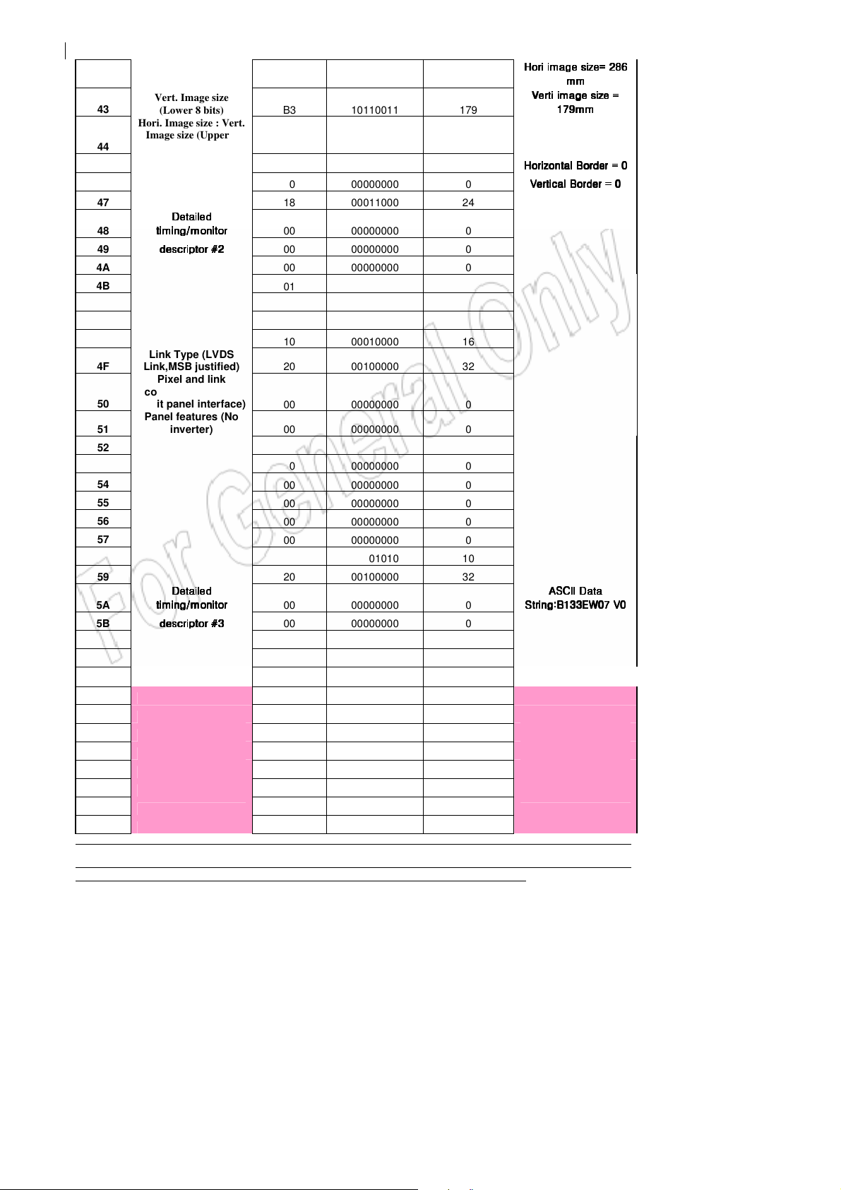
Hori image size= 286
Hori image size= 286
42
43
44
45
46
47
48
49
4A
4B
4C Version
4D edid signature
4E edid signature
4F
50
51
52
53
54
55
56
57
58
59
5A
5B
5C
5D
5E
5F
60
61
62
63
64
65
66
N
Hori. Image size
(Lower 8 bits) 1E 00011110 30
Vert. Image size
(Lower 8 bits) B3 10110011 179
Hori. Image size : Vert.
Image size (Upper 4
bits)
Detailed
Detailed
Detailed Detailed
timing/monitor
timing/monitor
timing/monitortiming/monitor
descriptor #2
descriptor #2
descriptor #2descriptor #2
00 00000000 0
Link Type (LVDS
Link,MSB justified)
Pixel and link
component format
(6-bit panel interface)
Panel features (No
inverter)
Detailed
Detailed
Detailed Detailed
timing/monitor
timing/monitor
timing/monitortiming/monitor
descriptor #3
descriptor #3
descriptor #3descriptor #3
www.jxlcd.com
www.jxlcd.com
33 00110011 51 3
57 01010111 87 W
10 00010000 16
00 00000000 0
00 00000000 0
18 00011000 24
00 00000000 0
00 00000000 0
01 00000001 1
00 00000000 0
06 00000110 6
10 00010000 16
20 00100000 32
00 00000000 0
00 00000000 0
00 00000000 0
00 00000000 0
00 00000000 0
00 00000000 0
00 00000000 0
00 00000000 0
0A 00001010 10
20 00100000 32
00 00000000 0
00 00000000 0
00 00000000 0
FE 11111110 254
00 00000000 0
42 01000010 66
31 00110001 49
33 00110011 51
45 01000101 69
30 00110000 48
37 00110111 55
Hori image size= 286 Hori image size= 286
mm
mm
mmmm
Verti image size =
Verti image size =
Verti image size = Verti image size =
179mm
179mm
179mm179mm
Horizontal Border = 0
Horizontal Border = 0
Horizontal Border = 0 Horizontal Border = 0
Vertical Border = 0
Vertical Border = 0
Vertical Border = 0 Vertical Border = 0
ASCII Data
ASCII Data
ASCII Data ASCII Data
String:B133EW07 V0
String:B133EW07 V0
String:B133EW07 V0String:B133EW07 V0
B
1
3
E
0
7
. | Size: A | METRIC | Scale: NONE | Page 19 of 55
Title: Spec, Elec., Dspl., AUO, 13.3” TFT-LCD DWG Number: 069-3542 Rev.01
Page 20
67
68
69
6A
6B
6C
6D
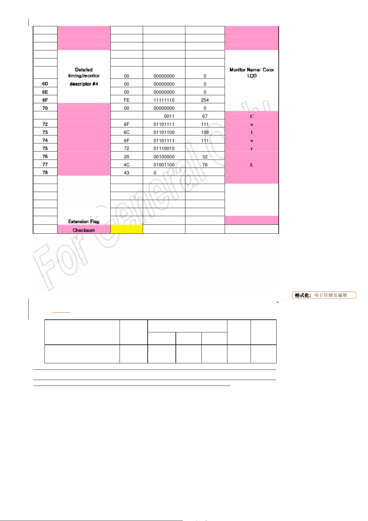
6E
6F
70
71
72
73
74
75
76
77
78
79
7A
7B
7C
7D
7E
7F
20 00100000 32
Detailed
Detailed
Detailed Detailed
timing/monitor
timing/monitor
timing/monitortiming/monitor
descriptor #4
descriptor #4
descriptor #4descriptor #4
6F 01101111 111 o
20 00100000 32
20 00100000 32
Extension Flag
Extension Flag
Extension FlagExtension Flag
Checks
Checksum
um
ChecksChecks
umum
56 01010110 86
30 00110000 48
0A 00001010 10
20 00100000 32
00 00000000 0
00 00000000 0
00 00000000 0
FE 11111110 254
00 00000000 0
43 01000011 67
6C 01101100 108
6F 01101111 111
72 01110010 114
4C 01001100 76
43 01000011 67
44 01000100 68
0A 00001010 10
20 00100000 32
20 00100000 32
00 00000000 0
13 00010011 19
V
0
Monitor Name: Color
Monitor Name: Color
Monitor Name: Color Monitor Name: Color
LCD
LCD
LCDLCD
C
l
o
r
L
C
D
www.jxlcd.com
www.jxlcd.com
4.7.5. Electrical Ratings
VALUES
PARAMETER SYMBOL
Min. Typ. Max.
Power Supply Input Voltage
N
. | Size: A | METRIC | Scale: NONE | Page 20 of 55
Title: Spec, Elec., Dspl., AUO, 13.3” TFT-LCD DWG Number: 069-3542 Rev.01
V
CC
3.0
3.3
3.6 V (DC)
UNIT NOTES
格格格格式化
式化::::
式化式化
項目符號及編號
Page 21
Power Supply Ripple
Power Supply Input Current
Differential Impedance
Power Consumption
Rush current
Notes: (1) The power supply ripple is measured whereas a black pattern is displayed;
(2) The specified current and power consumption are under the conditions at Vcc = 3.3 V, T =
25ºC, and fv = 60 Hz, f
(3) This impedance value is needed to a proper display and is measured from LVDS mating
connector to LVDS Rx
(4) The following is a typical Vcc circuit on the system side
3.3V
CONTROL SIGNAL
(HIGH to LOW)
12V
C3
1uF
www.jxlcd.com
www.jxlcd.com
Vcc rise time is about 470 µs
N
. | Size: A | METRIC | Scale: NONE | Page 21 of 55
Title: Spec, Elec., Dspl., AUO, 13.3” TFT-LCD DWG Number: 069-3542 Rev.01
I
CC
Zm
Pc
I
RUSH
=72.5MHz, whereas a mosaic pattern (typical) is displayed;
CLK
R1
47K
R2
1K
R3
47K
0.9Vcc
-
90
-
-
M1
2SK1059
C2
10000pF
M2
2SK1399
50
242
100
0.8
-
FUSE
273
110
0.9
1.5
C1
1uF
3.3V
470 µs
mV
mA
Ω
W
A
p-p
Vcc
1
2
3
2
4
(
LCD INPUT)
Page 22
4.7.6. Signal Timing
4.7.6.1. Signal Impedance
Defined in VESA standard for LVDS FPDI 2
4.7.6.2. Timing Data
This is the signal timing required at the input of the control ASIC concerned with
LVDS as a FlatLink or equivalent. All of the interface signal timing should be
satisfied with the following specifications based on the VESA timing guideline
(1280x800 @ 60 Hz) for its proper operation.
GND
The duration of the rush current is about 20 ms.
0.1Vcc
格格格格式化
式化::::
式化式化
格格格格式化
式化::::
式化式化
項目符號及編號
項目符號及編號
www.jxlcd.com
www.jxlcd.com
N
. | Size: A | METRIC | Scale: NONE | Page 22 of 55
Title: Spec, Elec., Dspl., AUO, 13.3” TFT-LCD DWG Number: 069-3542 Rev.01
Page 23
Video Timing Data
Signal Parameter Symbol Min Typ Max
D
Clock Period
CLK
Clock Frequency
Duty Ratio (% High)
Rise Time
Fall Time
DE
(Data Enable
Only)
(DTMG)
Data
H
H
sync
V
V
sync
Note: (1) When the WXGA+ controller sets DE Mode, and H
(DTMG) signal must be longer than 1 clock period (TC) at every horizontal sync period;
DE Setup Time
Data Setup Time
Data Hold Time
Horizontal Period
Horizontal Blank Period
Vertical Period
Vertical Blank Period
Back Porch
sync
H
Pulse Width
sync
H
Front Porch
sync
Horizontal Active Period
Back Porch
sync
V
Pulse Width
sync
V
Front Porch
sync
Vertical Active Period
www.jxlcd.com
www.jxlcd.com
T
T
T
H
T
Hfp
THD
V
TWV
Vfp
TVD
T
C
fC
Kdr
R CLK
F CLK
T
se
Tsd
Thd
TH
Tha
TV
wvb
bp
WH
bp
40
-
-
4
4
2
1280
800
sync
and V
13.79
72.50
50
4.42
4.42
-
-
-
1440
160
823
23
80
32
48
1280
14
6
3
800
are required. The duration of DE
sync
60
-
-
-
-
-
1280
800
Unit Note
ns
MHz
%
ns
ns
ns
ns
ns
TC
TC
TH
TH
T
C
TC
TC
TC
T
H
TH
TH
TH
1
1/T
TCh /TC
2
fV=59.94 Hz, 3
Display Period
Display Period
C
(2) Horizontal Period = One Line Scanning Time;
(3) The vertical period TV is related to the frame frequency fV, i.e., 60 Hz.
4.7.6.3. Video Timing Diagram
N
. | Size: A | METRIC | Scale: NONE | Page 23 of 55
Title: Spec, Elec., Dspl., AUO, 13.3” TFT-LCD DWG Number: 069-3542 Rev.01
格格格格式化
式化::::
式化式化
項目符號及編號
Page 24

1280 pixels
DE
DE
DEDE
DCLK
DCLK
DCLKDCLK
Da ta
Da ta
Da taDa ta
DE
DE
DEDE
T v d
Va lid
Va lid Dis play
Dis play Data
Va lidVa lid
Dis playDis play
T ch
T v
T hd
T h
Da t a ((((11111111 5555 2222p ix els )
Da t aDat a
T c
pix e ls )
pix e ls )pix e ls )
T w vb
T h s
90 %
50 %
DCLK
DCLK
DCLKDCLK
Display
Display
DisplayDis pla y
dat a
dat a
dat adat a
DE
DE
DEDE
N
. | Size: A | METRIC | Scale: NONE | Page 24 of 55
Title: Spec, Elec., Dspl., AUO, 13.3” TFT-LCD DWG Number: 069-3542 Rev.01
10 %
T r c lk
www.jxlcd.com
www.jxlcd.com
T ds
T e s
90 %
50 %
50 %
10 %
T fc lk
T dh
90 %
10 %
90 %
Page 25

4.7.7. Power Measurements (W/O backlight)
Pattern Min Typ Max Unit
格格格格式化
式化::::
式化式化
項目符號及編號
White To be updated
Mosaic 242 273 mA
V. Stripe To be updated
Black 273 303 mA
Note: (1) Display data pins and timing signal pins should be connected (GND = 0V);
(2) Operation conditions: fV = 60 Hz, f
(3) Power dissipation patterns are as follows.
(a) White screen (b) Mosaic (or checker) pattern
20x20 pixel black and white boxes
mA
mA
= 72.5 MHz, Vcc = 3.3 V;
CLK
Display Brightest Gray Level
Display Darkest Gray Level
(c) Vertical Stripe Pattern
sub-pixel vertical line on/off alternation,
www.jxlcd.com
www.jxlcd.com
N
. | Size: A | METRIC | Scale: NONE | Page 25 of 55
Title: Spec, Elec., Dspl., AUO, 13.3” TFT-LCD DWG Number: 069-3542 Rev.01
R G B R G B R G B
R G B R G B R G B
R G B R G B R G B
R G B R G B R G B
格格格格式化
式化::::
式化式化
項目符號及編號
Page 26

6
5
:
:
MacBook
4.7.8. Power on-off sequence
Power-on includes both system starting from power-off state and wake from sleep state;
power-off includes both system shutdown and entering sleep state.
Power on Power off Restart
刪除
刪除
刪除刪除
刪除
刪除
刪除刪除
MacBook
Power Supply for
LCD VCC
Interface Signal
(LVDS Signal of
Transmitter), Vi
Power for Lamp
90%
10%
0V
T
2
T
1
T3
Valid Data
ON
10
50
-
-
50
20
-
T
4
0V
OFF
Values Parameter
Min. Typ. Max.
T
1
T
2
T
3
T
4
www.jxlcd.com
T
5
www.jxlcd.com
T
6
T7
0.15
1
200
200
0
5
500
-
20
250
250
20
-
-
T
OFF
Unit
ms
ms
ms
ms
ms
ms
ms
T
90%
10%
T
7
4.7.9. Vcc Dip Condition
The Vcc dip is the Vcc voltage drop during panel start-up.
N
. | Size: A | METRIC | Scale: NONE | Page 26 of 55
Title: Spec, Elec., Dspl., AUO, 13.3” TFT-LCD DWG Number: 069-3542 Rev.01
格格格格式化
式化::::
式化式化
項目符號及編號
Page 27

:
5.4.8
(1) 2.5V ≤ Vcc < 3.0 V, Td ≤ 20 ms;
(2) For Vcc < 2.5V, Vcc should follow the power on-off sequence defined in 4.7.8
Vcc
td
刪除
刪除
刪除刪除
4.8. Near-Field Noise
The RF emissions from the panel (especially the LVDS input and Tcon) interfere with Wifi
operation.
Note that this spec compliance requirement is in addition to the legal EMI compliance
requirements.
4.9. Backlight Subsystem
4.9.1. General Information
LED Manufacturer Nichia
LED Manufacturer Assembly P/N Nichia NNSW208
www.jxlcd.com
www.jxlcd.com
Number of LEDs 54
LED Ranks V630 and up
LED Brightness Bin 50 mcd per bin
LED Vf Bin Rank 1 (2.8-3.0 V) and 2 (3.0-3.2 V)
格格格格式化
式化::::
式化式化
格格格格式化
式化::::
式化式化
項目符號及編號
項目符號及編號
LED Forward Voltage Range for All 6
LED Series Lines
4.9.2. Backlight Synchronization Requirement (to avoid BL shimmering)
N
. | Size: A | METRIC | Scale: NONE | Page 27 of 55
Title: Spec, Elec., Dspl., AUO, 13.3” TFT-LCD DWG Number: 069-3542 Rev.01
(Characterized at LVDS Connector for 23 mA)
MAX: 28.8 V
格格格格式化
式化::::
式化式化
項目符號及編號
Page 28

Display Minimum
The Vsync/STV signal is a once-per-frame pulse that has a constant phase delay with
respect to the start of the frame. This signal is used by the backlight LED driver to
synchronize BL PWM with the frame update to avoid shimmering (waterfall) artifacts in
the image.
The minimum pulse width is 1 us.
4.9.3. Backlight Electrical Characteristics
The backlight brightness test shall be tested at 600Hz PWM 94% cycle & 23 mA peak current
with following percentage duty cycle
LED Current (%
duty cycle)
94% 28.8 V 3.73 250 275 300
N
. | Size: A | METRIC | Scale: NONE | Page 28 of 55
Title: Spec, Elec., Dspl., AUO, 13.3” TFT-LCD DWG Number: 069-3542 Rev.01
www.jxlcd.com
www.jxlcd.com
LED Forward
Voltage for any
LED string
Power (W)
Assuming 3.2V
max forward bias
Luminance (nits)
Display Typical
Luminance (nits)
Display
Maximum
Luminance (nits)
格格格格式化
式化::::
式化式化
項目符號及編號
Page 29

19% 28.8 V 0.75 50 55 60
5% 28.8 V 0.19 12 14 15
4.9.4. LED Connection
String LED1 LED2 LED3 LED4 LED5 LED6 LED7 LED8 LED9
1
2
3
4
5
6
1 7 13 19 25 31 37 43 49
2 8 14 20 26 32 38 44 50
3 9 15 21 27 33 39 45 51
4 10 16 22 28 34 40 46 52
5 11 17 23 29 35 41 47 53
6 12 18 24 30 36 42 48 54
格格格格式化
式化::::
式化式化
項目符號及編號
www.jxlcd.com
www.jxlcd.com
N
. | Size: A | METRIC | Scale: NONE | Page 29 of 55
Title: Spec, Elec., Dspl., AUO, 13.3” TFT-LCD DWG Number: 069-3542 Rev.01
Page 30

5. OPTICAL REQUIREMENTS
5.1. Optical Specifications
Supplier must submit optical measurement data from 20 samples for items marked critical in
Table 6.1.1. The optical performance will be based on supplier’s measurement data, visual
inspection of the samples, verification measurements, and specification correlation.
Table 6.1.1: Optical Characteristics
Parameter Symbol
Iso-Contrast Viewing Angle
CR ≥ 10
Contrast ratio CR Optimal 400 600 -- -- 1,2,3
Luminance Y I
Global Luminance Uniformity Optimal 50 -- % 1,2
Worst Neighbor Luminance
Uniformity
Gamma
Flicker F No Visual Flicker
Cross Talk D
Worst Low Level (dark)
Inversion Viewing Direction
Response (rise+fall time)
Gray to Gray Response time
www.jxlcd.com
www.jxlcd.com
θ
down 45 50
left/right 55/55 60/60
Optimal 80 -- % 1,2
γ
Optimal -- 2.0 % 1,2,3
SHA
PCB on the
τ
θ = 0°, Ta=25°C
on+off
τ
θ = 0°, Ta=25°C
G2G
Condition Min. Typ. Max. Unit Note
up 45 50 -- Degrees 1,2,3
=23 mA
LED
@94% duty cycle
-- -- 2.2 -- -- 1,2,3
bottom
220 250 -- cd/m2 1,2,4
-- -- -30 dB 1,2,3
-- 6:00 -- o’clock 1,2
-- 16 25 ms 1,2,3
-- 40 ms 1,2,3
x CIE 1931 0.297 0.313 0.329 -- 1,2,3 White Chromaticity
(all panels)
(Within one panel)
N
. | Size: A | METRIC | Scale: NONE | Page 30 of 55
Title: Spec, Elec., Dspl., AUO, 13.3” TFT-LCD DWG Number: 069-3542 Rev.01
y 0.313 0.329 0.345 -- 1,2,3
delta x 0.005 White Chromaticity
delta y 0.008
x CIE 1931 0.620 0.640 0.660 -- 1,2,3 Red Chromaticity
y 0.315 0.330 0.345 -- 1,2,3
Page 31

Parameter Symbol
Green Chromaticity
Max color difference within
one panel
Max color difference w.r.t.
Center within one panel
Max color difference from
panel to panel
Max color difference between
neigbors
Note 1: The testing conditions are specified in 6.2.
Note 2: The definitions of optical characteristics are shown in 6.3.
Note 3: Measured at center point. Equivalent performance over the entire panel required.
Note 4: Both center point and average of 160 points.
x CIE 1931 0.290 0.310 0.330 -- 1,2,3
Y 0.590 0.610 0.630 -- 1,2,3
X CIE 1931 0.120 0.150 0.170 -- 1,2,3 Blue Chromaticity
Y 0.040 0.060 0.080 -- 1,2,3
du’v’ white 0.005 1,2
du’v’ white 0.003 1,2
du’v’ white 0.008
du’v’ white 0.0025
Condition Min. Typ. Max. Unit Note
1,2
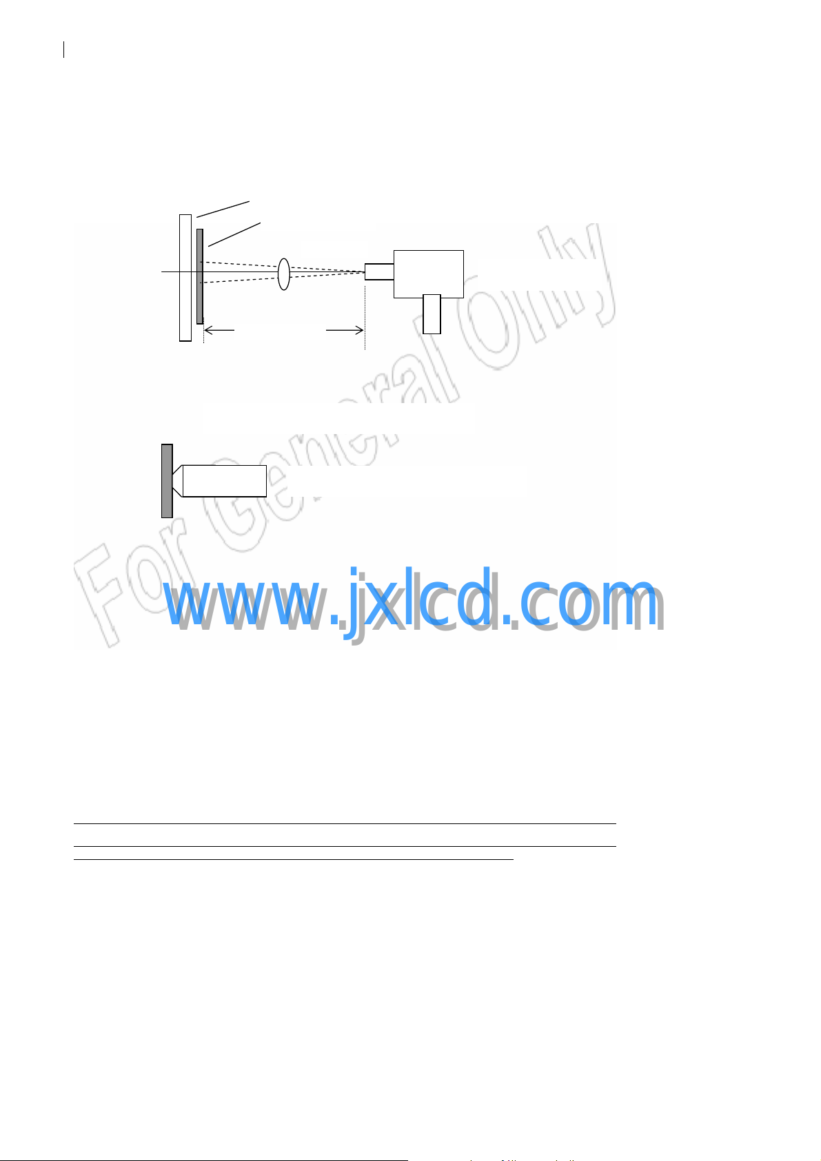
5.2. Measuring Conditions
The optical characteristics are determined after the unit has been ‘ON’ and stable for
approximately 30 minutes at the maximum brightness, in a dark environment at an
ambient temperature at 25°C ± 2°C. The electrical conditions include Vcc = 3.3 V, fv =
60 Hz, f
measuring equipments for luminance and color are CCD based imaging systems such as
Radiant Imaging Prometric 1400 system, or Colorimeter such as Photo Research PR650,
TOPCON BM-5A or similar. The measuring distance should be about 50 cm from the
LCD surface at normal unless otherwise specified. Measurements should be done on the
160 grid points as shown in the following figures. The measurement spot at the center is
approximately 12 mm in diameter from a distance of 400 mm by TOPCON BM-5A or
15 mm in diameter from a distance of 500 mm by PR 650.
Viewing angle measurements should be done by an Eldim EZ Color system or similar.
N
. | Size: A | METRIC | Scale: NONE | Page 31 of 55
Title: Spec, Elec., Dspl., AUO, 13.3” TFT-LCD DWG Number: 069-3542 Rev.01
= 72.5 MHz, IBL = 23 mA @94% duty cycle with 600Hz. Recommended
CLK
www.jxlcd.com
www.jxlcd.com
Page 32
Field = 2
°
The CIE 1931 or 1976 Standards will be used.
Luminance and Color Measurement
X-Y Stage
LCD Module
TOPCON BM-5A
or PR650 or CCD
400 or 500 mm
Viewing Angle Measurement
ELDIM EZ Color or equivalent
Figure 6-1: Optical Measurement Set-up
N
. | Size: A | METRIC | Scale: NONE | Page 32 of 55
Title: Spec, Elec., Dspl., AUO, 13.3” TFT-LCD DWG Number: 069-3542 Rev.01
www.jxlcd.com
www.jxlcd.com
Page 33
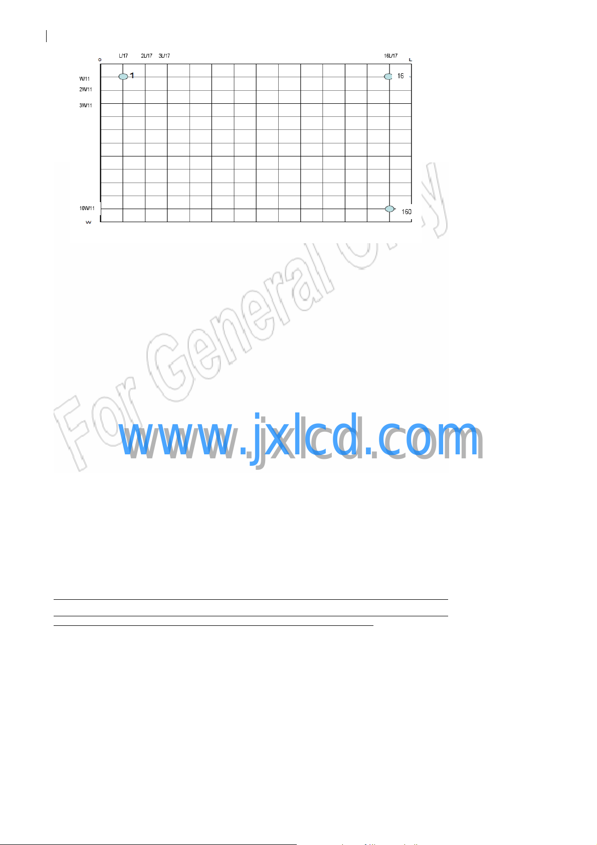
Figure 6-2: Measurement point location. L and W are the length and width of Active Area
respectively.
5.3. Definition
5.3.1. Center Point Luminance
Lct =(L
5.3.2. Average Luminance
L
5.3.3. Luminance Uniformity
5.3.3.1. Global Luminance Uniformity:
N
. | Size: A | METRIC | Scale: NONE | Page 33 of 55
Title: Spec, Elec., Dspl., AUO, 13.3” TFT-LCD DWG Number: 069-3542 Rev.01
72+ L73+ L88+ L89
= SUM(L1:L
Ave
where L1 to L
www.jxlcd.com
www.jxlcd.com
The entire display active area shall be scanned with the luminance measurement
with white screen set full brightness.
two kinds of data for brightness uniformity: Luminance Uniformity, and Worst
Neighbor Luminance Uniformity. The definitions are shown in below:
160
U = 100% - (L
where, L
)/4{Average Luminance value at point #72, 73, 88, 89}
) / 160
160
are the luminance values measured at point #1 to #160.
)/L
max-Lmin
= max {Luminance values at 160 points},
max
max
Page 34
L
= min {Luminance values at 160 points}
min
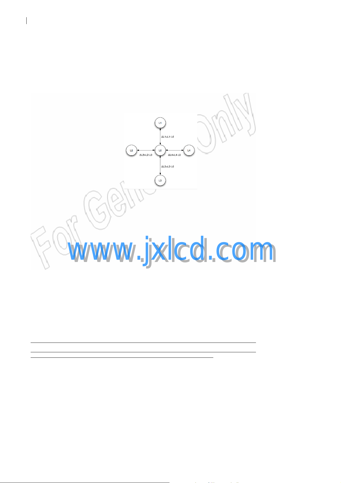
5.3.3.2. Worst Neighbor Luminance Uniformity (The 4 points that are closest to
the test point)
WNU=100%-Max(∆L1, ∆L2, ∆L3, ∆L4)/L0
Global WNU = min (WNU1, …WNU160)
5.3.4. Contrast Ratio
CR = Luminance at G
#72, 73, 88, 89}
5.3.5. White Color Uniformity
The entire display active area shall be scanned with the color coordinate
www.jxlcd.com
www.jxlcd.com
measurement with white screen set full brightness.
5.3.5.1. Panel to Panel White Color Uniformity
The center point (as defined by the average value at point #72, 73, 88, 89) white
color coordinate of any panel shall be within the box with 4 corners coordination
boundary listed in Table 6.1.
N
. | Size: A | METRIC | Scale: NONE | Page 34 of 55
Title: Spec, Elec., Dspl., AUO, 13.3” TFT-LCD DWG Number: 069-3542 Rev.01
/ Luminance at G
max
{Average contrast value at point
min
Page 35
5.3.5.2. Max Color Difference with respect to the center within a panel
On each panel, the maximum color difference between any of the 160 points and
the center point (defined as the average value at point #72, 73, 88, 89),
represented in delta u’v’.
5.3.5.3. Max Color Difference between any two points within the panel
On each panel, the maximum color difference between any two of the 143 points ,
represented in delta u’v’.
5.3.5.4. Max Color Difference between two neighbors
On each panel, the maximum color difference between any two neighboring
points on the panel, represented in delta u’v’
5.3.6. RGB Color Chromaticity
The entire display active area shall be scanned with the color coordinate
measurement with screen set to full brightness and solid R, G, B color
respectively. The measured color coordinate of any panel shall be within the box
with 4 corners coordination boundary listed in Table 6.1.
5.3.7. Viewing Angle
The viewing angle is defined as the viewing angle range under the condition at
CR > 10:1 .
φ
L
Normal Line
o
φ = 0
,
θ = 0
φ
H
o
θ
R
12 O’clock
direction
y
φ H = 90o
x'y'
o
θR =90
www.jxlcd.com
www.jxlcd.com
θ
L
o
θ L =90
6 O’clock
direction
φ L= 90o
N
. | Size: A | METRIC | Scale: NONE | Page 35 of 55
Title: Spec, Elec., Dspl., AUO, 13.3” TFT-LCD DWG Number: 069-3542 Rev.01
x
Page 36
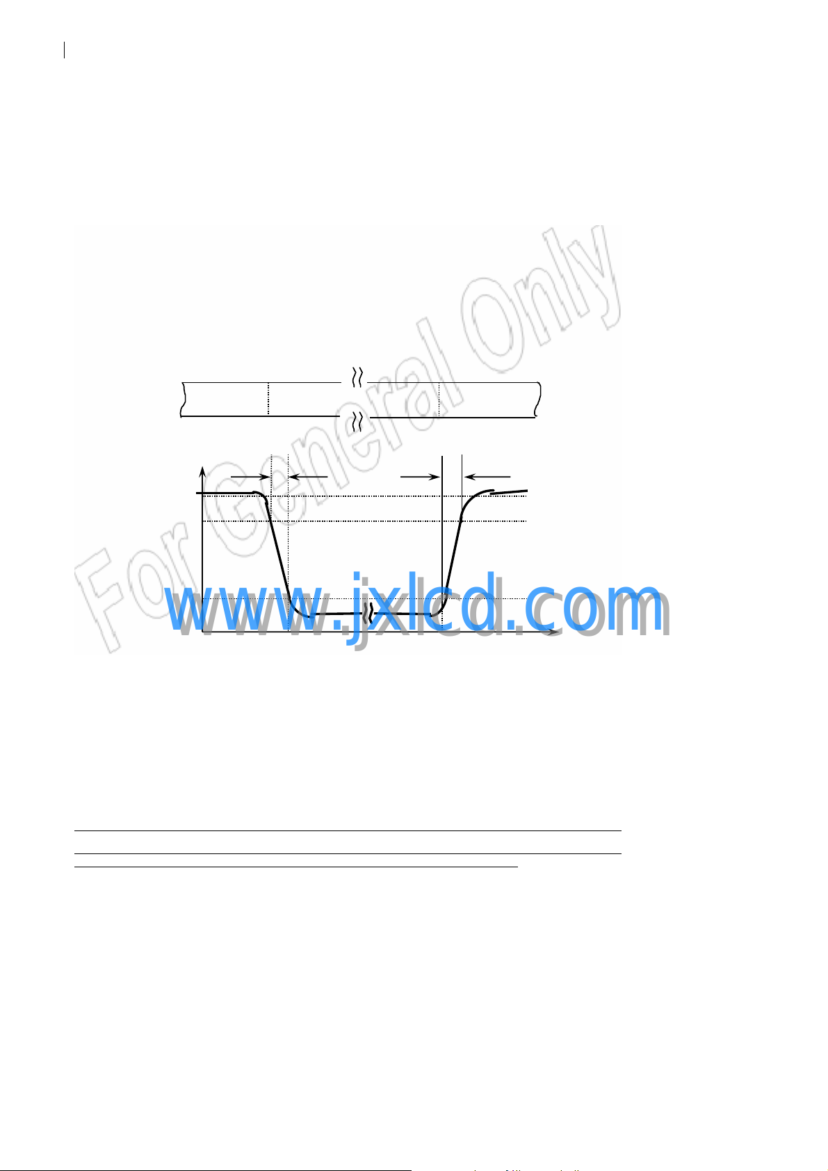
Figure 6-4: Viewing angle definition
5.3.8. Gray Scale Inversion
Luminance vs. viewing angle curves are measured based on gray level 255, 223,
191, 159, 127, 95, 63, 32 and 0, in the viewing angle of left, right, up, down, with
PCB on the bottom side. Gray scale inversion happens when a higher gray scale
measures the same luminance or lower luminance than any of the lower gray scale.
5.3.9. Response Time
5.3.9.1. On and Off Response Time
The On/Off response time, tR + tF, is defined in the following figure and shall be
measured by switching the input signal for “black” and “white”.
s
Display data
Optical
Response
5.3.9.2. Gray to Gray Response Time
White (TFT OFF)
100%
90%
10%
0%
www.jxlcd.com
www.jxlcd.com
Figure 6-5: Response Time Measurement
Gray to Gray Response Time is measured in a similar method. But instead of
switching display between black and white, panel is switched between two gray
scales. The maximum gray-to-gray response time is based on 9 levels of gray
t
R
Black (TFT ON)
White (TFT OFF)
t
F
Time
N
. | Size: A | METRIC | Scale: NONE | Page 36 of 55
Title: Spec, Elec., Dspl., AUO, 13.3” TFT-LCD DWG Number: 069-3542 Rev.01
Page 37
scales. The 9 levels are: gray level 255, 223, 191, 159, 127, 95, 63, 32 and 0.
Figure 6-6 shows an example of Gray to Gray Response Time measurement data.
Response護Tim
e
50
40
30
[ms]
20
10
255
223
191
Start Gray scale
159
127
95
63
32
0 0
32
63
127
95
159
Arrival Gray scale
0
255
223
191
Figure 6-6: Gray to Gray Response Time
5.3.10. Gray Scale Linearity or Gamma Value
The display luminance, LG, is measured at the different gray scales, G
min
, …, G
max
.
The exponential fitting is used to determine the gamma (γ) value, which should be
an intrinsic or uncorrected characteristic.
www.jxlcd.com
www.jxlcd.com
LG ~ Gϒ.
5.3.11. Flicker
No visual flicker will be allowed. The flicker level should be measured with
either vertical stripes or a checker pattern, defined in Sec. 5.3.6. The output signal
of a photometer is sent to an FFT analyzer. The flicker is essentially a ratio of the
powers in the frequency spectrum at 30 Hz (Px) and 0 Hz (P0), i.e.,
N
. | Size: A | METRIC | Scale: NONE | Page 37 of 55
Title: Spec, Elec., Dspl., AUO, 13.3” TFT-LCD DWG Number: 069-3542 Rev.01
Page 38
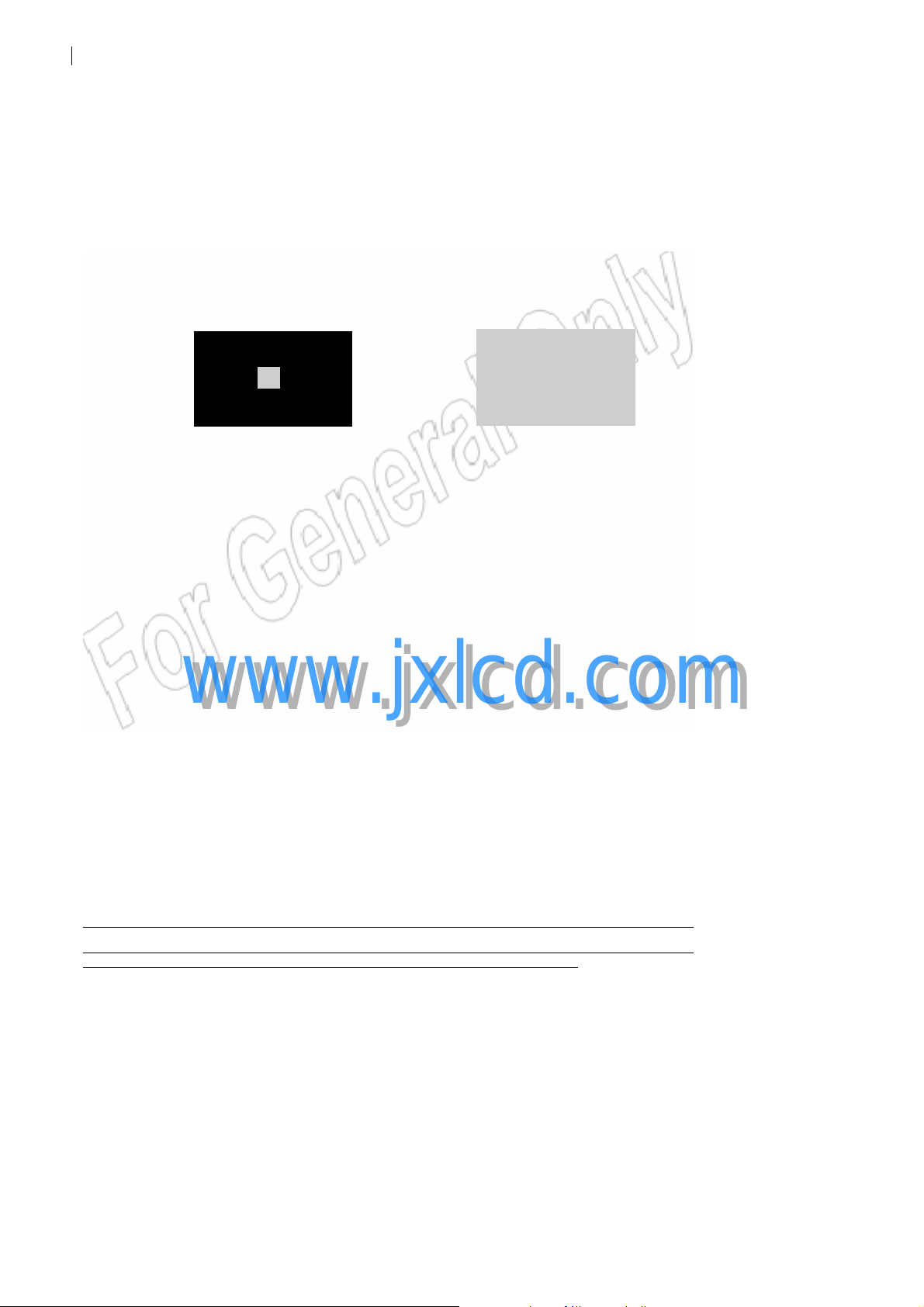
Black in surrounding
le = 127/255 in center
F = 10 Log (Px / P0).
5.3.12. Cross-talk
No visual cross-talk will be allowed. Two luminance values are measured at
center spot with 50 x 50 pixels. The cross-talk, D
D
= (LB – LA)/LB • 100%,
SHA
Where, LA = Luminance in Pattern A
LB = Luminance in Pattern B.
Pattern A
Gray Sca
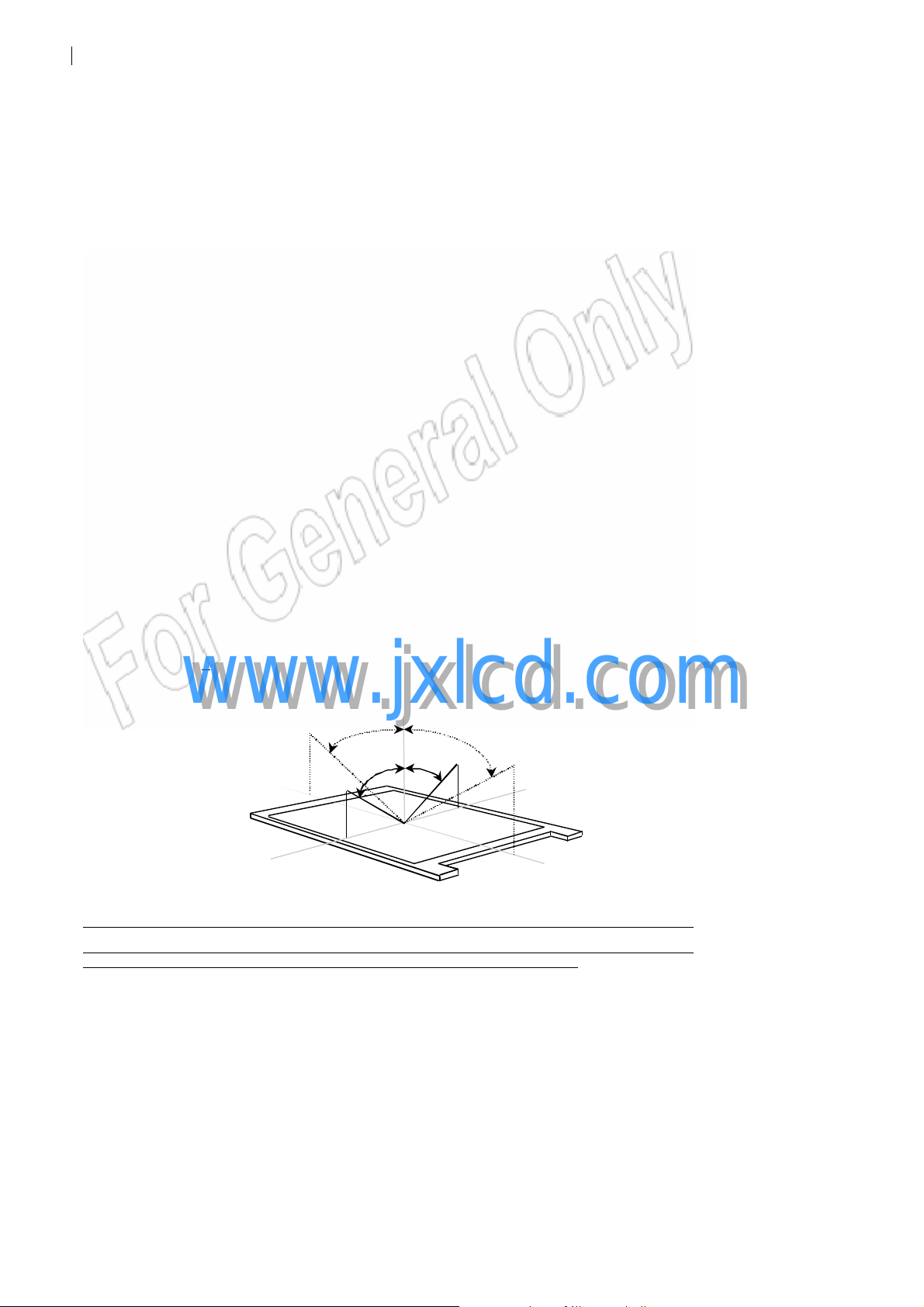
5.4. Hot Spot Specifications:
The LED hot spot shall be inspected from 70 degree to -40 degree per the drawing
below. There shall be no visible hot spot or no worse than “limited sample” hot spot (if
, is defined as,
SHA
Pattern B
Gray Scale = 127/255 full screen
there is a “limited sample” set up.
www.jxlcd.com
www.jxlcd.com
N
. | Size: A | METRIC | Scale: NONE | Page 38 of 55
Title: Spec, Elec., Dspl., AUO, 13.3” TFT-LCD DWG Number: 069-3542 Rev.01
Page 39

www.jxlcd.com
www.jxlcd.com
N
. | Size: A | METRIC | Scale: NONE | Page 39 of 55
Title: Spec, Elec., Dspl., AUO, 13.3” TFT-LCD DWG Number: 069-3542 Rev.01
Page 40

:
e
6. ENVIRONMENTAL
The display modules shall meet all functional and cosmetic specifications after testing to the
nvironmental quality standards listed in this section. Additionally, the LCD modules in products
shall pass all the system testing requirements listed in the end of this document.
6.1. Shock and Vibration
7.1.1 There will be no functional or cosmetic defects following a shock to all 6 sides
delivering at least 200 G in a half sine pulse no longer than 2 ms to the display
module, secured by its designated mounting details, in accordance with MIL-STD-
202F Method 213B, test condition A.
7.1.2 There will be no functional defects following a shock delivering at least 260 g in a
half sine pulse no longer than 2 ms to each of 6 sides. Each of the 6 sides will be
shock tested with one each display, for a total of 6 displays. The displays are secured
by designated mounting details, in accordance with MIL-STD-202F Method 213B,
test condition A.
刪除
刪除
刪除刪除
7.1.3 There will be no functional or cosmetic defects following a shock delivering at least
60 G in a pulse 11 msec or longer to the display module, secured by its designated
mounting details, in accordance with MIL-STD-202F Method 213B, test condition A.
7.1.4 There shall be no functional or cosmetic defects following a vibration test,
conducted at 3.0 G from 5–150 Hz, 0.37 Oct/min with sine wave for 30 min./axis,
with the display secured by its designated mounting details, and conducted in
accordance with MIL-STD-202F, method 201A.
www.jxlcd.com
www.jxlcd.com
N
. | Size: A | METRIC | Scale: NONE | Page 40 of 55
Title: Spec, Elec., Dspl., AUO, 13.3” TFT-LCD DWG Number: 069-3542 Rev.01
Page 41

30%
6.2. Temperature and Humidity
Unless otherwise stated in this specification, the display module must meet functional
and cosmetic requirements after testing in accordance with Spec. # 080-0859, non-
operating and operating conditions.
For these tests, the following limits set forth in Specification #080-0859 shall be altered
to read.
6.2.1. General Performance Requirements
60
90%
80%
50%
-25 0 10 20 30
Note:
1) Maximum wet bulb temp operating temperature is 39°C.
2) Maximum wet bulb temp storage temperature is 48°C.
Wet Bulb
Temperature
39
30
20
10
0
www.jxlcd.com
www.jxlcd.com
Dry Bulb Temperature [°C]
50
48
40
40 50 60 70 80
40%
20%
10%
Humidity [%(RH)]
+
Storage
Operation
N
. | Size: A | METRIC | Scale: NONE | Page 41 of 55
Title: Spec, Elec., Dspl., AUO, 13.3” TFT-LCD DWG Number: 069-3542 Rev.01
Page 42

6.2.2. Non-operational Testing
6.2.2.1. Low Temperature
-25°C @ 500 hrs
6.2.2.2. High Temperature
65°C @ 500 hrs
6.2.2.3. High Temperature and High Humidity
60°C @ 500 hrs, R.H. = 75% ± 10%
6.2.2.4. Thermal Shock
Cycle display from -25°C to 65°C with 5-minute transfer time,
100 cycles at -25°C/65°C/-25°C.
6.2.3. Operational Testing
6.2.3.1. Low Temperature
0°C for 500 hours
6.2.3.2. High Temperature
50°C for 500 hours
www.jxlcd.com
www.jxlcd.com
6.2.3.3. High Temperature and High Humidity
50°C and 90% R.H. for 240 hours (Functional Check)
Maximum wet-bulb temperature at 39°C or lower without
condensation.
6.2.3.4. Four Corner Test (72 hrs – operating)
40°C @ 10% RH
40°C @ 90% RH
N
. | Size: A | METRIC | Scale: NONE | Page 42 of 55
Title: Spec, Elec., Dspl., AUO, 13.3” TFT-LCD DWG Number: 069-3542 Rev.01
Page 43

10°C @10% RH
10°C @ 90% RH
6.3. Altitude
72 hour storage
Operational: 15,000 Ft.
Non-Operational: 40,000 Ft.
7. RELIABILITY
7.1. Resistance to Normal Abuse
7.1.1. Torsion Test
Module is fixed by 4 mounting holes (A, B, & C) on stable supports. Tester is
connected to mounting hole on free floating module corner. Push/Pull test is
conducted on all four corners.
7.1.2. Test Conditions:
Applied Force 20 N
Cycles 10 K
Frequency (F=push / pull)1 Hz (1 cycle / sec.)
www.jxlcd.com
www.jxlcd.com
N
. | Size: A | METRIC | Scale: NONE | Page 43 of 55
Title: Spec, Elec., Dspl., AUO, 13.3” TFT-LCD DWG Number: 069-3542 Rev.01
Page 44

7.1.3. Test Set-up
7.1.4. Static Load Deflection and Breakage
Supplier shall demonstrate compliance per Specification 062-2208 Static
Breakage Test
7.2. Electrostatic Discharge (ESD)
Display modules are to be tested for ESD susceptibility per specification 062-
0302. The display modules must meet the Level 1 for the bare module, and Level
1 through III test requirements stated in the above referenced specification, when
assembled in a portable computer.
www.jxlcd.com
7.3. MTBF
N
. | Size: A | METRIC | Scale: NONE | Page 44 of 55
Title: Spec, Elec., Dspl., AUO, 13.3” TFT-LCD DWG Number: 069-3542 Rev.01
www.jxlcd.com
Supplier to demonstrate display module meets minimum 50,000 Hrs.@90%
Confidence Supplier to include any acceleration factors included in the
calculations. Power cycling frequency during this test is to be approved.
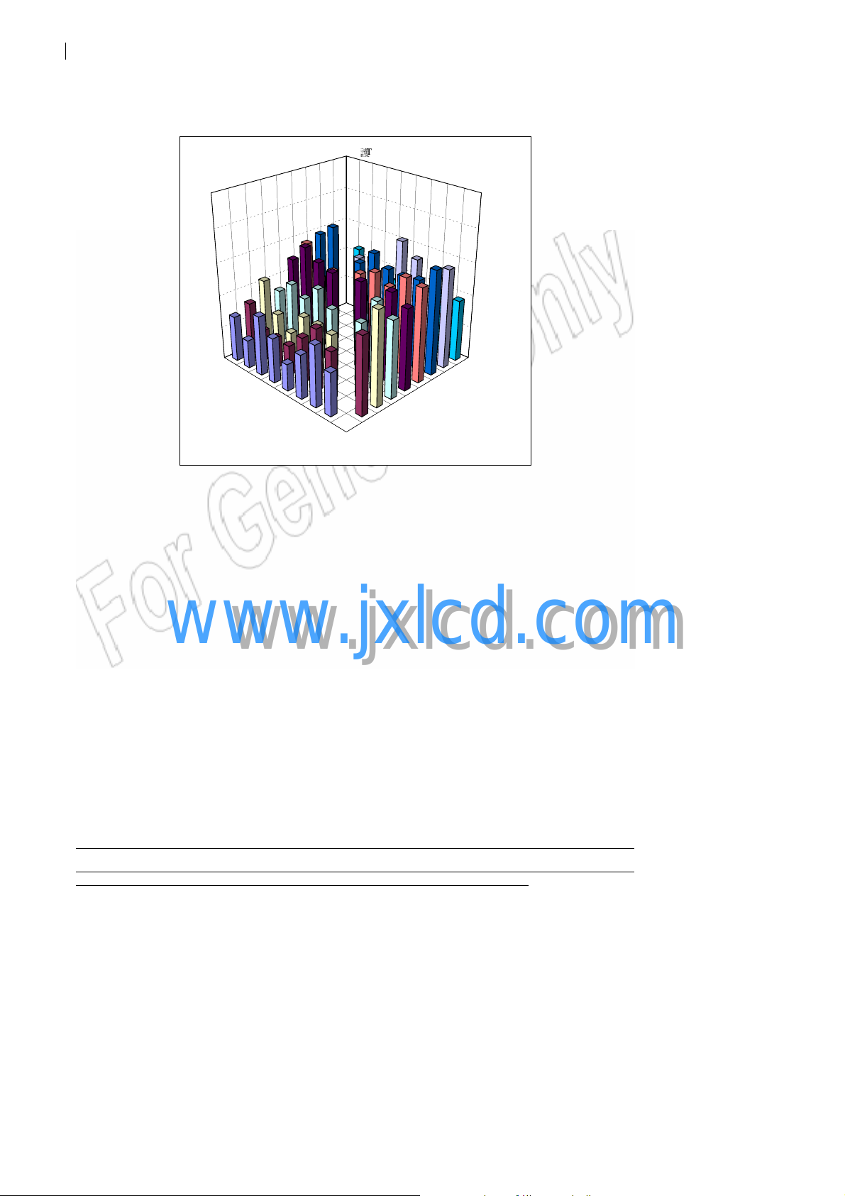
Page 45

7.4. LCD Glass Strength
The LCD glass strength (failure load) will be defined at a single 90% survival rate value on
Weibull distribution. Please provide the optimized loading performance in the similar chart
format below. The failure load of the 90% Weibull survival rate shall be higher than TBD N.
Probability Plot for bendload
Complete Data - LSXY Estimates
99
90
80
70
60
50
40
30
20
Percent
10
The 4 point bend test shall be used for the LCD glass strength test. The detailed fixture design/
shall follow the ASTM standard C158-02. The fixture is used in conduction with a load-
displacement machine, commonly known as Instron.
EXAMPLE ONLY
5
3
2
1
Bending Load (Newton)
bendload
Weibull
Table of Statistics
Shape
Scale 0.0024863
Mean 0.0023964
StDev 0.0002073
Median 0.0024227
IQR 0.0 002677
Failure 22
Censor 0
AD* 1. 220
Correlation 0.972
0.00280.00260.00240.00220.00200.0018
14.1433
www.jxlcd.com
www.jxlcd.com
N
. | Size: A | METRIC | Scale: NONE | Page 45 of 55
Title: Spec, Elec., Dspl., AUO, 13.3” TFT-LCD DWG Number: 069-3542 Rev.01
Page 46

Two orientations must be tested for this specification: orientation A (Figure 2.A) and orientation B
(Figure 2.B)
This test shall be performed on 30 samples, WITH current POLARIZERS laminated on both top
www.jxlcd.com
www.jxlcd.com
and bottom of the LCD glass, per applicable orientation as a First Article Inspection and when
settings, tooling, and equipment are modified. Supplier is responsible for monitoring glass strength
on an ongoing production basis. The test shall be conducted with a top rollers velocity of 1 mm/min.
As soon as the first plane breaks, the test shall be stopped to prevent the second plane from
breaking.
N
. | Size: A | METRIC | Scale: NONE | Page 46 of 55
Title: Spec, Elec., Dspl., AUO, 13.3” TFT-LCD DWG Number: 069-3542 Rev.01
Page 47

Orientation A. Longer plane parallel to ledge Orientation B. Shorter plane parallel to ledge
Figure 2. Display orientations measuring strength at edges
LCD glass strength data collection
Failure initiation site must be determined by visual inspection by selecting one of the different cases shown below
(Figure 3).
Case A) If the failure is starting from the bottom edge or close to it, enter letter A.
Case B) If the failure is starting from the top edge or close it, enter letter B.
Case C) If the failure is starting from the surface of glass, away from the edges and showing branching in both
directions, enter letter C.
Case D) When testing in orientation D (Figure 1.D), if the failure is starting at the epoxy region between the panes,
enter letter C edges of the glass (case D).
Case E) If during testing a snap is heard, but no crack is visible, enter letter E
Case O) If the failure does not match any of the above or cannot be easily recognized due to catastrophic breakage,
enter letter O.
www.jxlcd.com
www.jxlcd.com
N
. | Size: A | METRIC | Scale: NONE | Page 47 of 55
Title: Spec, Elec., Dspl., AUO, 13.3” TFT-LCD DWG Number: 069-3542 Rev.01
Page 48

a [mm] =
Site Case (A, B, C,
D, E, or O)
26
Initiation site
Initiation site
Initiation site
OR
OR
OR
Small branching
Small branching
Small branching
near edge
near edge
near edge
Case A. Failure from bottom edge (with or without slight branching near edge)
OR
Initiation site
Initiation site
OR
Small branching
Small branching
near edge
near edge
Initiation site
Initiation site
Case B. Failure from top edge (with or without slight branching near edge)
Initiation site
Initiation site
Initiation site
Epoxy
Epoxy
www.jxlcd.com
www.jxlcd.com
Approximate
Approximate
initiation site
initiation site
Ledge
Ledge
Failure
Failure
Approximate
Approximate
initiation
initiation
initiation site
initiation site
site
site
Case C. Initiation on surface of glass Case D. Failure at surface on epoxy region (Orientation D)
Figure 3 Surface crack initiation.
All failure loads and failure initiation sites will be entered in the following table below.
N
. | Size: A | METRIC | Scale: NONE | Page 48 of 55
Title: Spec, Elec., Dspl., AUO, 13.3” TFT-LCD DWG Number: 069-3542 Rev.01
Orientation a b c d (Circle one)
W [mm] = Llong [mm] =
Lshort [mm] = t [mm] =
Unit # Failure Load [N]
1
2
3
4
5
6
7
8
9
10
11
12
13
14
15
16
17
18
19
20
21
22
23
24
25
Failure Initiation
Page 49

N
. | Size: A | METRIC | Scale: NONE | Page 49 of 55
Title: Spec, Elec., Dspl., AUO, 13.3” TFT-LCD DWG Number: 069-3542 Rev.01
www.jxlcd.com
www.jxlcd.com
Page 50

8. COSMETIC REQUIREMENTS
Cosmetic Specification for Notebook Display, 062-7003E.
www.jxlcd.com
www.jxlcd.com
N
. | Size: A | METRIC | Scale: NONE | Page 50 of 55
Title: Spec, Elec., Dspl., AUO, 13.3” TFT-LCD DWG Number: 069-3542 Rev.01
Page 51

9. REGULATORY
9.1. Product Safety (Environmental, Ergonomics, Safety and Health)
Materials: specific chemical composition information or certifications necessary for the
product to enter countries, markets, and/or for component(s) material identification, or for
to respond to customer requests for information. The information may be in the form of,
but is not limited to, Material Safety Data Sheets, material specification sheets, health
hazard information, certifications, or other forms of documentation.
9.2. RoHS Compliance and other Substance Regulations
This product’s components, parts, and packaging shall be manufactured or assembled
based upon the following requirements.
10.2.1 The display module must comply with the European RoHS directive, As evidence
of such compliance, the supplier must provide a declaration of conformity in
accordance with RoHS Declaration of Conformity Procedure, 080-2153.
10.2.2 In addition to RoHS compliance, the display module and its manufacturing
process shall comply with Regulated Substances Specification, 069-0135.
10.2.3 The vendor shall provide a written statement declaring the average and maximum
amount of mercury in the display module.
10.3 Halogen Free
www.jxlcd.com
Flat panel display must be must be halogen-free in accordance with the Halogen-Free
Specification, 069-1857
9.3. Environmental Markings and Recycling
10.3.1 Flat panel display must be modular in design so that parts can be easily separated,
N
. | Size: A | METRIC | Scale: NONE | Page 51 of 55
Title: Spec, Elec., Dspl., AUO, 13.3” TFT-LCD DWG Number: 069-3542 Rev.01
www.jxlcd.com
without any special tools, for ease of proper recycling/disposal at the product's
end-of-life.
Page 52

10.3.2 Flat panel display plastic parts >25 grams must be marked according to ISO
11469 (except for the LGP (light guide panel) and optical films in the backlight).
9.4. Product Safety
Flat panel display assembly shall comply with Specification,
069-0279, Product Safety Requirements for Component Flat Panel Display
Assemblies.
9.5. Ergonomics
The flat panel display must comply with the ergonomic requirements of ISO 13406 parts
1 and 2. The vendor shall provide a written statement that the flat panel display, is
certified to comply with ISO 13406, parts 1 and 2.
9.6. Electromagnetic Compatibility (EMC)
10.6 Emissions
The final product must meet Class B Emission Standards for home electronic
device when configured within a system Spec. #062-0718. The display supplier
must provide all necessary support as required to meet this requirement. EMI
measurements are taken at the worst-case contrast setting.
www.jxlcd.com
10.6.1 Susceptibility
10.6.2 Spectrum Spreading Compatibility (SSC)
N
. | Size: A | METRIC | Scale: NONE | Page 52 of 55
Title: Spec, Elec., Dspl., AUO, 13.3” TFT-LCD DWG Number: 069-3542 Rev.01
www.jxlcd.com
Performance degradation due to external noise or RF will be considered as
specified in #062-0718 for Class B products.
10.6.2.1 Emissions
The final product must be compatible with spectrum spreading conditions
specified in 1.2.2 of this document. No failure or degradation in electronic
Page 53

functionality and optical performance is allowed with the spreading turned
ON compared to that when it is turned OFF.
10.6.2.2 Conditions for Spectrum Spreading
Spreading %: 0% (min.), 0.75% (typical), and 1.5% (max.)
Spreading type: center or down
Modulation Rate: 40 to 80 kHz.
www.jxlcd.com
www.jxlcd.com
N
. | Size: A | METRIC | Scale: NONE | Page 53 of 55
Title: Spec, Elec., Dspl., AUO, 13.3” TFT-LCD DWG Number: 069-3542 Rev.01
Page 54

11 FACTORY/SERVICE REQUIREMENTS
11.1 SQBR
Factory requirements are outlined in Supplier Quality and Business Requirements,
specification 070-1191.
11.6 SERVICE REQUIREMENTS
Service Requirements are outlined in specification 070-0385.
www.jxlcd.com
www.jxlcd.com
N
. | Size: A | METRIC | Scale: NONE | Page 54 of 55
Title: Spec, Elec., Dspl., AUO, 13.3” TFT-LCD DWG Number: 069-3542 Rev.01
Page 55

12 REFERENCE DOCUMENTS
www.jxlcd.com
www.jxlcd.com
N
. | Size: A | METRIC | Scale: NONE | Page 55 of 55
Title: Spec, Elec., Dspl., AUO, 13.3” TFT-LCD DWG Number: 069-3542 Rev.01
 Loading...