

Page 1

Product Specification
) Preliminary Specifications
(V
( ) Final Specifications
Module
Model Name
12.1” WXGA Color TFT-LCD
B121EW04 V1
B121EW04 V1
Customer Date
www.jxlcd.com
www.jxlcd.com
Checked &
Approved by
Note: This Specification is subject to change
without notice.
Approved by Date
Howard Lee
Prepared by
Weitse Hsu
NBBU Marketing Division /
AU Optronics corporation
2007/10/12
2007/10/12
document version 0.1 1
PDF created with pdfFactory Pro trial version www.pdffactory.com
Page 2

Product Specification
B121EW04 V1
Contents
1. Handling Precautions..............................................................................................................4
2. General Description.................................................................................................................5
2.1 General Specification.........................................................................................................5
2.2 Optical Characteristics.......................................................................................................6
3. Functional Block Diagram.....................................................................................................11
4. Absolute Maximum Ratings..................................................................................................12
4.1 Absolute Ratings of TFT LCD Module..............................................................................12
4.2 Absolute Ratings of Backlight Unit...................................................................................12
4.3 Absolute Ratings of Environment.....................................................................................12
5. Electrical characteristics.......................................................................................................13
5.1 TFT LCD Module..............................................................................................................13
5.2 Backlight Unit...................................................................................................................15
6. Signal Characteristic.............................................................................................................16
6.1 Pixel Format Image..........................................................................................................16
6.2 The input data format.......................................................................................................17
6.3 Signal Description/Pin Assignment..................................................................................18
6.4 Interface Timing................................................................................................................20
6.5 Power ON/OFF Sequence...............................................................................................21
7. Connector Description..........................................................................................................22
8. Vibration and Shock Test......................................................................................................23
8.1 Vibration Test...................................................................................................................23
8.2 Shock Test Spec:..............................................................................................................23
9. Reliability................................................................................................................................24
10. Mechanical Characteristics.................................................................................................25
11. Shipping and Package.........................................................................................................27
11.1 Shipping Label Format...................................................................................................27
11.2. Carton package.............................................................................................................27
11.3 Shipping package of palletizing......................................................................................28
12. Appendix: EDID description................................................................................................29
www.jxlcd.com
www.jxlcd.com
document version 0.1 2
PDF created with pdfFactory Pro trial version www.pdffactory.com
Page 3

Product Specification
B121EW04 V1
Record of Revision
Version and Date Page
0.1 2007/09/27 All First Edition for Customer
Old description New Description Remark
www.jxlcd.com
www.jxlcd.com
document version 0.1 3
PDF created with pdfFactory Pro trial version www.pdffactory.com
Page 4

Product Specification
B121EW04 V1
1. Handling Precautions
1) Since front polarizer is easily damaged, pay attention not to scratch it.
2) Be sure to turn off power supply when inserting or disconnecting from input connector.
3) Wipe off water drop immediately. Long contact with water may cause discoloration or spots.
4) When the panel surface is soiled, wipe it with absorbent cotton or other soft cloth.
5) Since the panel is made of glass, it may break or crack if dropped or bumped on hard surface.
6) Since CMOS LSI is used in this module, take care of static electricity and insure human earth when
handling.
7) Do not open nor modify the Module Assembly.
8) Do not press the reflector sheet at the back of the module to any directions.
9) In case if a Module has to be put back into the packing container slot after once it was taken out
from the container, do not press the center of the LED Reflector edge. Instead, press at the far ends
of the CFL Reflector edge softly. Otherwise the TFT Module may be damaged.
10) At the insertion or removal of the Signal Interface Connector, be sure not to rotate nor tilt the
Interface Connector of the TFT Module.
11) After installation of the TFT Module into an enclosure (Notebook PC Bezel, for example), do not
twist nor bend the TFT Module even momentary. At designing the enclosure, it should be taken into
consideration that no bending/twisting forces are applied to the TFT Module from outside.
Otherwise the TFT Module may be damaged.
12) Cold cathode fluorescent lamp in LCD contains a small amount of mercury. Please follow local ordinances
or regulations for disposal.
13) Small amount of materials having no flammability grade is used in the LCD module. The LCD module
should be supplied by power complied with requirements of Limited Power Source (IEC60950 or UL1950),
or be applied exemption.
14) The LCD module is designed so that the LED in it is supplied by Limited Current Circuit (IEC60950 or
UL1950). Do not connect the LED in Hazardous Voltage Circuit.
www.jxlcd.com
www.jxlcd.com
document version 0.1 4
PDF created with pdfFactory Pro trial version www.pdffactory.com
Page 5

Product Specification
B121EW04 V1
2. General Description
B121EW04 V2 is a Color Active Matrix Liquid Crystal Display composed of a TFT LCD panel, a driver circuit,
LED backlight system, and a digitizer unit. The screen format is intended to support the WXGA (1280(H) x
800(V)) screen and 262k colors (RGB 6-bits data driver). All input signals are LVDS interface compatible.
B121EW04 V2 is designed for a display unit of tablet style personal computer and industrial machine.
2.1 General Specification
The following items are characteristics summary on the table at 25 ℃ condition:
Items Unit Specifications
Screen Diagonal [mm] 307.9 (12.1 W”)
Active Area [mm] 261.12 (H) x 163.2 (V)
Pixels H x V 1280x3(RGB) x 800
Pixel Pitch [mm] 0.204
Pixel Arrangement R.G.B. Vertical Stripe
Display Mode Normally White
White Luminance (ILED=20.0mA)
Note: ILED is lamp current
[cd/m2] 220 Typ. (5 points average)
200 Min. (5 points average)
(Note1)
Luminance Uniformity 1.25 max. (5 points)
Contrast Ratio 600:1 Typ.,500:1 Min.
Optical Rise Time/Fall Time [msec] 25 Typ., 35 Max.
Nominal Input Voltage VDD [Volt] +3.3 Typ.
Power Consumption [Watt] 5.5 Max. (Inculding logic and BLU power,with LED
Weight (w/o Inverter) [Grams] 220g Max.
Physical Size [mm]
Electrical Interface 1 channel LVDS
Surface Treatment Anti-galre, 3H
Support Color 262K colors ( RGB 6-bit )
Temperature Range
Operating
Storage (Non-Operating)
RoHS Compliance RoHS Compliance
www.jxlcd.com
www.jxlcd.com
circuit loss) @ 20.0 mA
L W T
Max 294.1 178.5 3.5
Typ 293.6 178.0 3.15
min 293.1 177.5 -
[oC]
[oC]
0 to +50
-20 to +60
document version 0.1 5
PDF created with pdfFactory Pro trial version www.pdffactory.com
Page 6

Product Specification
B121EW04 V1
2.2 Optical Characteristics
The optical characteristics are measured under stable conditions at 25℃ (Room Temperature):
Item Unit Conditions Min. Typ. Max. Note
White Luminance
ILED=20.0mA
Viewing Angle
Luminance Uniformity
Luminance Uniformity
CR: Contrast Ratio
Cross talk %
Response Time
Color / Chromaticity
Coordinates
www.jxlcd.com
www.jxlcd.com
(CIE 1931)
[cd/m2]
[degree]
[degree]
[degree]
[degree]
[msec] Rising
[msec] Falling
[msec] Rising + Falling
5 points average
Horizontal (Right)
CR = 10 (Left)
Vertical (Upper)
CR = 10 (Lower)
5 Points
13 Points
500 600 - 6
1.4 7
Red x
Red y
Green x
Green y
Blue x
Blue y
White x
White y
220 250 - 1, 4, 5.
70
70
70
70
1.25 1
1.80 2
-
- 10 15
25 35
0.550 0.580 0.610
0.310 0.340 0.370
0.300 0.330 0.360
0.545 0.575 0.605
0.125 0.155 0.185
0.105 0.135 0.165
0.283 0. 313 0.343
0.299 0.329 0.359
80
80
80
80
15
-
-
-
-
20
8
8
2,8
NTSC [%] CIE 1931 - 45 -
document version 0.1 6
PDF created with pdfFactory Pro trial version www.pdffactory.com
Page 7

Product Specification
= Maximum Brightn
ess of thirteen points
Minimum Brightness of thirteen points
Maximum Brightness of five points
= Minimum Brightness of five points
Note 1: 5 points position (Display area: 261.12 (H) x 163.2 (V) mm)
Note 2: 13 points position
H/4
H/4
H
H/4
H/4
B121EW04 V1
W
W/4 W/4 W/4 W/4
1 2
3
4 5
www.jxlcd.com
www.jxlcd.com
Note 3: The luminance uniformity of 5 and 13 points is defined by dividing the maximum luminance values by
the minimum test point luminance
δ
W5
δ
W13
document version 0.1 7
PDF created with pdfFactory Pro trial version www.pdffactory.com
Page 8

Product Specification
Field=2
°
Contrast ratio (CR)=
Brightness on the “White” state
Brightne
ss on the “Black” state
Note 4: Measurement method
The LCD module should be stabilized at given temperature for 30 minutes to avoid abrupt temperature
change during measuring. In order to stabilize the luminance, the measurement should be executed
after lighting Backlight for 30 minutes in a stable, windless and dark room.
B121EW04 V1
Photo detector
Note 5: Definition of Average Luminance of White (YL):
Note 6: Definition of contrast ratio:
www.jxlcd.com
www.jxlcd.com
Measure the luminance of gray level 63 at 5 points,Y
L (x) is corresponding to the luminance of the point X at Figure in Note (1).
Contrast ratio is calculated with the following formula.
= [L (1)+ L (2)+ L (3)+ L (4)+ L (5)] / 5
L
document version 0.1 8
PDF created with pdfFactory Pro trial version www.pdffactory.com
Page 9

Product Specification
"Black"
Tr
Tf "White"
"White"
0 % 10 % 90 % 100 %
Note 7: Definition of Cross Talk (CT)
CT = | YB – YA | / YA × 100 (%)
Where
YA = Luminance of measured location without gray level 0 pattern (cd/m2)
YB = Luminance of measured location with gray level 0 pattern (cd/m2)
B121EW04 V1
Note 8: Definition of response time:
The output signals of BM-7 or equivalent are measured when the input signals are changed from
“Black” to “White” (falling time) and from “White” to “Black” (rising time), respectively. The response
time interval between the 10% and 90% of amplitudes. Refer to figure as below.
www.jxlcd.com
www.jxlcd.com
document version 0.1 9
PDF created with pdfFactory Pro trial version www.pdffactory.com
Page 10

Product Specification
Note 9: Definition of viewing angle
Viewing angle is the measurement of contrast ratio ≧10, at the screen center, over a 180° horizontal
and 180° vertical range (off-normal viewing angles). The 180° viewing angle range is broken down as
follows; 90° (θ) horizontal left and right and 90° (Φ) vertical, high (up) and low (down). The
measurement direction is typically perpendicular to the display surface with the screen rotated about its
center to develop the desired measurement viewing angle.
B121EW04 V1
www.jxlcd.com
www.jxlcd.com
document version 0.1 10
PDF created with pdfFactory Pro trial version www.pdffactory.com
Page 11

Product Specification
B121EW04 V1
3. Functional Block Diagram
The following diagram shows the functional block of the 12. 1inches wide Color TFT/LCD Module with
touch panel:
www.jxlcd.com
www.jxlcd.com
document version 0.1 11
PDF created with pdfFactory Pro trial version www.pdffactory.com
Page 12

Product Specification
B121EW04 V1
4. Absolute Maximum Ratings
Absolute maximum ratings of the module are as following:
4.1 Absolute Ratings of TFT LCD Module
Item Symbol Min Max Unit Conditions
Logic/LCD Drive
4.2 Absolute Ratings of Backlight Unit
Item Symbol Min Max Unit Conditions
LED Current ILED - 20.0 [mA] rms Note 1,2
4.3 Absolute Ratings of Environment
Item Symbol Min Max Unit Conditions
Operating Temperature
Operation Humidity HOP 5 95 [%RH] Note 3
Storage Temperature
Storage Humidity HST
Note 1: At Ta (25℃)
VDD -0.3 +4.0 [Volt] Note 1,2
TOP 0 +50 [oC] Note 3
TST -20 +60 [oC] Note 3
5 95
[%RH]
Note 3
Note 2: Permanent damage to the device may occur if exceed maximum values
Note 3: For quality performance, please refer to AUO IIS(Incoming Inspection Standard).
Twb=39° C
www.jxlcd.com
www.jxlcd.com
Operating Range Storage Range
document version 0.1 12
PDF created with pdfFactory Pro trial version www.pdffactory.com
Page 13
Product Specification
90% 10%
B121EW04 V1
5. Electrical characteristics
5.1 TFT LCD Module
5.1.1 Power Specification
Input power specifications are as follows;
Symble Parameter Min Typ Max Units Note
VDD Logic/LCD Drive
Voltage
PDD VDD Power 1.3 1.5 [Watt] Note 1
IDD IDD Current 400 420 [mA]
IRush Inrush Current
VDDrp Allowable
Logic/LCD Drive
Ripple Voltage
VDDns Allowable
Logic/LCD Drive
Ripple Noise
3.0 3.3 3.6 [Volt]
1800 [mA]
500 [mV]
p-p
100 [mV]
p-p
Note 1
Note 2
Note 1: Maximum Measurement Condition:Black Pattern
Note 2: Measure Condition
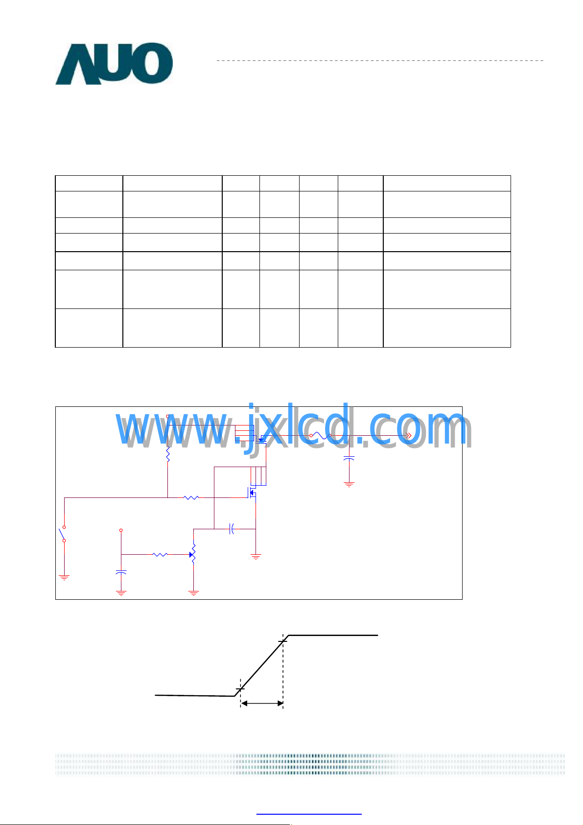
Q3
AO6402
D6 F1
D5
D2 S
D1
G
D2SD1D5
D6
Q3
G
C3
0.01uF/25V
AO6402
SW1
SW MAG-SPST
1 2
+3.3V
www.jxlcd.com
www.jxlcd.com
(High to Low)
Control
Signal
+12.0V
C2
1uF/25V
R1
47K
R2
1K
R2
1K
VR1
47K
(LCD Module Input)
C1
1uF/16V
3.3V
VCC
0V
0.5ms
Vin rising time
document version 0.1 13
PDF created with pdfFactory Pro trial version www.pdffactory.com
Page 14

Product Specification
B121EW04 V1
5.1.2 Signal Electrical Characteristics
Input signals shall be low or High-impedance state when VDD is off.
Signal electrical characteristics are as follows;
Parameter Condition Min Max Unit
Vth
Vtl
Vcm
Note: LVDS Differential Voltage
Differential Input High
Threshold (Vcm=+1.2V)
Differential Input Low
Threshold (Vcm=+1.2V)
Differential Input Common
Mode Voltage
-100
0.3
100
2.2
[mV]
[mV]
[V]
www.jxlcd.com
www.jxlcd.com
document version 0.1 14
PDF created with pdfFactory Pro trial version www.pdffactory.com
Page 15

Product Specification
5.2 Backlight Unit
Parameter guideline for LED Inverter
Parameter Min Typ Max Units Condition
White Luminance
5 points average
LED current(I
LED Frequency(F
LED Voltage (Reference)
(V
LED
LED Power consumption
(P
) @ 20.0 mA
LED
) 18.8 20.0 21.2 [mA] rms
LED
) - 800 - [KHz]
LED
)
B121EW04 V1
220 250
3.0 3.2 3.3
- 3.6 4.0
-
[cd/m2 ]
[Volt] rms
[Watt]
(Ta=25 )℃
(Ta=25)℃
(Ta=25)℃
(Ta=25)℃
(Ta=25)℃
(Including circuit driving
loss)
www.jxlcd.com
www.jxlcd.com
document version 0.1 15
PDF created with pdfFactory Pro trial version www.pdffactory.com
Page 16

Product Specification
R G B R G B R G B R G B R G B R G B 0 1
B121EW04 V1
6. Signal Characteristic
6.1 Pixel Format Image
Following figure shows the relationship of the input signals and LCD pixel format.
1st Line
R G B R G B
1278 1279
800th Line
www.jxlcd.com
www.jxlcd.com
document version 0.1 16
PDF created with pdfFactory Pro trial version www.pdffactory.com
Page 17

Product Specification
6.2 The input data format
Signal Name
+RED5 (R5)
+RED4 (R4)
+RED3 (R3)
+RED2 (R2)
+RED1 (R1)
+RED0 (R0)
Description
Red Data 5 (MSB)
Red Data 4
Red Data 3
Red Data 2
Red Data 1
Red Data 0 (LSB)
(Red-pixel Data)
B121EW04 V1
Red-pixel Data
Each red pixel's brightness data consists of these 6
bits pixel data.
+GREEN 5 (G5)
+GREEN 4 (G4)
+GREEN 3 (G3)
+GREEN 2 (G2)
+GREEN 1 (G1)
+GREEN 0 (G0)
+BLUE 5 (B5)
+BLUE 4 (B4)
+BLUE 3 (B3)
+BLUE 2 (B2)
+BLUE 1 (B1)
+BLUE 0 (B0)
-DTCLK
DSPTMG (DE)
VSYNC (VS) Vertical Sync The signal is synchronized to -DTCLK .
HSYNC (HS) Horizontal Sync The signal is synchronized to -DTCLK .
Note: Output signals from any system shall be low or High-impedance state when VDD is off.
www.jxlcd.com
www.jxlcd.com
Green Data 5 (MSB)
Green Data 4
Green Data 3
Green Data 2
Green Data 1
Green Data 0 (LSB)
(Green-pixel Data)
Blue Data 5 (MSB)
Blue Data 4
Blue Data 3
Blue Data 2
Blue Data 1
Blue Data 0 (LSB)
(Blue-pixel Data)
Data Clock
Display Timing
Green-pixel Data
Each green pixel's brightness data consists of these
6 bits pixel data.
Blue-pixel Data
Each blue pixel's brightness data consists of these 6
bits pixel data.
The typical frequency is 71.1 MHz. The signal is used
to strobe the pixel data and DSPTMG signals. All
pixel data shall be valid at the falling edge when the
DSPTMG signal is high.
This signal is stored at the falling edge of -DTCLK.
When the signal is high, the pixel data shall be valid
to be displayed.
document version 0.1 17
PDF created with pdfFactory Pro trial version www.pdffactory.com
Page 18

Product Specification
B121EW04 V1
6.3 Signal Description/Pin Assignment
LVDS (CN1) is a differential signal technology for LCD interface and high speed data transfer device.
Pin Signal Name Pin Signal Name
1 GND 2 VDD
3 VDD 4 V
5 Aging 6 CLK
7 DATA
9 RxIN0+ 10 GND
11 RxIN1- 12 RxIN1+
13 GND 14 RxIN215 RxIN2+ 16 GND
17 RxCLKIN- 18 RxCLKIN+
19 GND 20 NC
21 NC 22 GND
23 NC 24 NC
25 GND 26 NC
8 RxIN0-
EDID
EDID
EDID
27 NC 28 GND
29 NC 30 NC
LED driving connector (CN2) provides the interface between system and LCD for control and power of LED
BLU.
www.jxlcd.com
www.jxlcd.com
Pin Signal Name Pin Signal Name
1 KS10 2 KS11
3 KS12 4 KS13
5 KS17 6 KSC18
7 GND 8 Power SW
9 Breath PWR LED 10 +3.3V
11 GND 12 LCD SMDCLK
13 LCD SMB DAT 14 GND
15 HDD LED 16 BAT2 LED
17 BAT1 LED 18 BT LED
19 LED WLAN OUT 20 GND
21 AUD DMIC IN0 22 AUO DMIC CLK_G
23 VL 24 VL
25 VL 26 V_5
27 NC 28 VH
29 VH 30 VH
document version 0.1 18
PDF created with pdfFactory Pro trial version www.pdffactory.com
Page 19

Product Specification
R R R
9
12
15 17 18 8
Note1: Start from right side
Pin 1
KS10
B121EW04 V1
CN1
CN2
Pin 30
VH
Pin 30
NC
Pin 1
GND
Note2: Input signals shall be low or High-impedance state when VDD is off.
Internal circuit of LVDS inputs are as following.
The module uses a 100ohm resistor between positive and negative data lines of each receiver input
www.jxlcd.com
www.jxlcd.com
Signal Input
Pin No.
11
14
RxIN0-
RxIN0+
RxIN1-
RxIN1+
RxIN2-
RxIN2+
RxCLKIN-
RxCLKIN+
R
LVDS Receiver
document version 0.1 19
PDF created with pdfFactory Pro trial version www.pdffactory.com
Page 20

Product Specification
B121EW04 V1
6.4 Interface Timing
6.4.1 Timing Characteristics
Basically, interface timings should match the 1280x800 /60Hz manufacturing guide line timing.
Parameter Symbol Min. Typ. Max. Unit
Frame Rate - 60 - Hz
Clock frequency 1/ T
Period T
Vertical
Active T
Section
Blanking T
Period T
Horizontal
Active T
Section
Blanking T
Note: DE mode only
71.1 MHz
Clock
V
VD
VB
H
HD
HB
803 823 1023
800 800 800
3 23 223
1303 1440 2047
1280 1280 1280
23 160 767
T
T
Clock
Line
6.4.2 Timing diagram
DOTCLK
T
CLOCK
www.jxlcd.com
www.jxlcd.com
Input
Data
DE
DE
Invaild
Data
T
HB
Input Timing Definition ( DE Mode)
Pixel
1
T
VB
Pixel
2
T
Pixel
3
T
HD
H
T
V
Pixel
N-1
T
VD
Pixel
N
Invaild
Data
Pixel
1
document version 0.1 20
PDF created with pdfFactory Pro trial version www.pdffactory.com
Page 21

Product Specification
T3 T2
T1
T7
B121EW04 V1
6.5 Power ON/OFF Sequence
VDD power and lamp on/off sequence is as follows. Interface signals are also shown in the chart. Signals from
any system shall be Hi-Z state or low level when VDD is off.
Power Supply VDD
Power Sequence Timing
Backlight On
www.jxlcd.com
www.jxlcd.com
90%
10%
Parameter
T1 0.5 - 10 (ms)
T2 0 - 50 (ms)
T3 0 - 50 (ms)
T4 400 - - (ms)
T5 200 - - (ms)
Min. Typ. Max.
T5
Value
VALID
DATA
90%
10%
T4
T6
Units
T6 200 - - (ms)
T7 0 - 10 (ms)
document version 0.1 21
PDF created with pdfFactory Pro trial version www.pdffactory.com
Page 22

Product Specification
B121EW04 V1
7. Connector Description
Physical interface is described as for the connector on module.
These connectors are capable of accommodating the following signals and will be following components.
Connector Name / Designation LVDS (CN1)/ LED BLU (CN2)
Manufacturer
Type / Part Number
Mating Housing/Part Number
Mating Contact/Part Number
JAE
JAE FI-J30S-VF15N
JAE FI-J30C3
JAE FI-J30C3
www.jxlcd.com
www.jxlcd.com
document version 0.1 22
PDF created with pdfFactory Pro trial version www.pdffactory.com
Page 23

Product Specification
B121EW04 V1
8. Vibration and Shock Test
8.1 Vibration Test
Test Spec:
l Test method: Non-Operation
l Acceleration: 1.5G , sine wave
l Frequency: 10 - 500Hz Random
l Sweep: 0.5 octave/minute in each of three mutually perpendicular axes.
8.2 Shock Test Spec:
Test Spec:
l Test method: Non-Operation
l Acceleration: 180 G , Half sine wave
l Active time: 2 ms
l Pulse: Half sine wave
www.jxlcd.com
www.jxlcd.com
document version 0.1 23
PDF created with pdfFactory Pro trial version www.pdffactory.com
Page 24

Product Specification
B121EW04 V1
9. Reliability
Subject Description
Operating High Temperature
Operating Low Temperature
Storage High Temperature
Storage Low Temperature
High Temp &High Humidity
Temperature Cycling
Non-Operating
+50℃ ,Dynamic ,250hr ,Humity 20%
0℃ ,Dynamic ,250hr ,Humity 20%
+65℃ ,Non_Operating ,250hr ,Humity 20%
-20℃ ,Non_Operating ,250hr
+40℃ ,Dynamic ,Humidity 95% ,250hr
-40℃ to +65℃ ,Ramp< 20℃ /min, Duration at Temp. = 30 min,
Test Cycles =50
Altitude
MTBF 200K hrs
www.jxlcd.com
Storage Shock
Storage Vibration
ESD
Note1:
Self-recoverable. No hardware failures.
Note2:
According to EN61000-4-2, ESD class B: Some performance degradation allowed. No data lost.
MTBF (Excluding the LED): 20,000 hours with a confidence level 90%.
www.jxlcd.com
Op(0~14000 ft)
Non-op (0~40000ft)
180g’s, 2.0 ms, Half Sine Wave ± 3 Axis ( +X, -X, +Y, -Y, +Z, -Z)
1Shocks per Direction
1.5 Grms, 30 min/side, PSD Spectrum Break Points, 26 Hz
G2/Hz=0.316, 50 Hz G2/Hz=0.007, 222 Hz G2/Hz=0.0018, 500Hz
G2/Hz=0.0001
Contact : ±8 KV
Air : ±15 KV
document version 0.1 24
PDF created with pdfFactory Pro trial version www.pdffactory.com
Page 25

Product Specification
10. Mechanical Characteristics
B121EW04 V1
www.jxlcd.com
www.jxlcd.com
document version 0.1 25
PDF created with pdfFactory Pro trial version www.pdffactory.com
Page 26

Product Specification
B121EW04 V1
www.jxlcd.com
www.jxlcd.com
document version 0.1 26
PDF created with pdfFactory Pro trial version www.pdffactory.com
Page 27

Product Specification
0AXXG
90mm
B121EW04 V1
11. Shipping and Package
11.1 Shipping Label Format
AUO LCD S/N Label: This label records the model name, firmware/ hardware version, manufacture date, and
serial number of the LCD in AUO.
Manufactured 05/52
Model No: B121EW04
AU Optronics
MADE IN TAIWAN (M1)
V1
C US
E204356
H/W: 0A F/W:1
Pb
RoHS
35mm
11.2. Carton package
The outside dimension of carton is 423(L)mm* 374(W)mm* 335(H)mm, carton and cushion weight are 1800g.
Maximum quantity of each carton is 20 pcs LCD.
www.jxlcd.com
www.jxlcd.com
document version 0.1 27
PDF created with pdfFactory Pro trial version www.pdffactory.com
Page 28
Product Specification
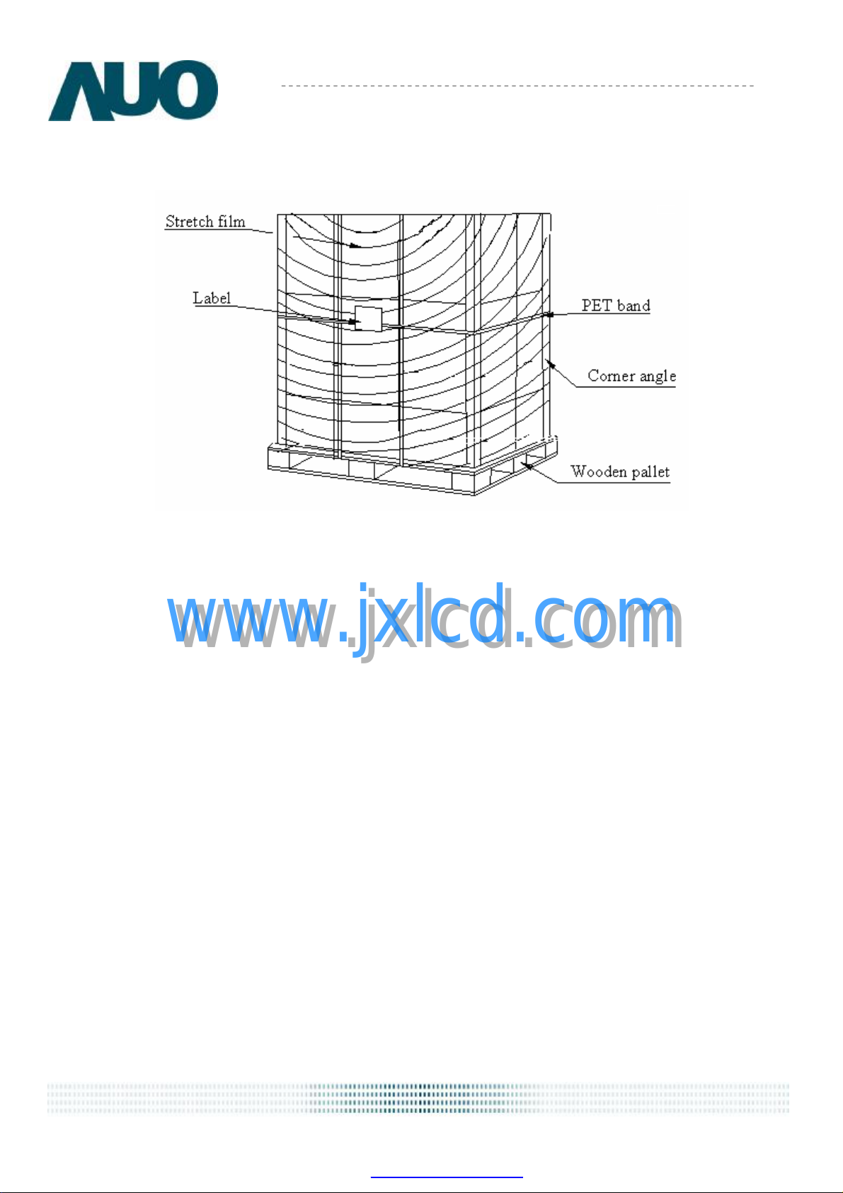
11.3 Shipping package of palletizing
B121EW04 V1
www.jxlcd.com
www.jxlcd.com
document version 0.1 28
PDF created with pdfFactory Pro trial version www.pdffactory.com
Page 29

Product Specification
B121EW04 V1
12. Appendix: EDID description
FUNCTION
HEX
00 Header 00 00000000 0
01 Header FF 11111111 255
02 Header FF 11111111 255
03 Header FF 11111111 255
04 Header FF 11111111 255
05 Header FF 11111111 255
06 Header FF 11111111 255
07 Header 00 00000000 0
08 EISA manufacture code = 3 Character ID 06 00000110 6
09 EISA manufacture code (Compressed ASCII) AF 10101111 175
Value Value Value
(hex) (binary) (DEC)
0A Panel Supplier Reserved – Product Code 14 00010100 20
0B Panel Supplier Reserved – Product Code 42 01000010 66
LCD module Serial No - Preferred but Optional (“0” if not
0C
used) 00 00000000 0
LCD module Serial No - Preferred but Optional (“0” if not
0D
used) 00 00000000 0
LCD module Serial No - Preferred but Optional (“0” if not
0E
used) 00 00000000 0
LCD module Serial No - Preferred but Optional (“0” if not
0F
used) 00 00000000 0
10 Week of manufacture 01 00000001 1
11 Year of manufacture 11 00010001 17
12 EDID structure version # = 1 01 00000001 1
13 EDID revision # = 3 03 00000011 3
14 Video I/P definition = Digital I/P (80h) 80 10000000 128
15 Max H image size = (Rounded to cm) 1A 00011010 26
www.jxlcd.com
www.jxlcd.com
16 Max V image size = (Rounded to cm) 10 00010000 16
Display gamma = (gamma ×100)-100
17
Example: ( 2.2×100 ) – 100 = 120 78 01111000 120
18 Feature support ( no DPMS, Active off, RGB, timing BLK 1) 0A 00001010 10
19 Red/Green Low bit (RxRy/GxGy) 89 10001001 137
1A Blue/White Low bit (BxBy/WxWy) E5 11100101 229
document version 0.1 29
PDF created with pdfFactory Pro trial version www.pdffactory.com
Page 30

Product Specification
1B Red X 94 10010100 148
1C Red Y 57 01010111 87
1D Green X 54 01010100 84
1E Green Y 93 10010011 147
1F Blue X 27 00100111 39
20 Blue Y 22 00100010 34
21 White X 50 01010000 80
22 White Y 54 01010100 84
23 Established timings 1 (00h if not used) 00 00000000 0
24 Established timings 2 (00h if not used) 00 00000000 0
25 Manufacturer’s timings (00h if not used) 00 00000000 0
26 Standard timing ID1 (01h if not used) 01 00000001 1
27 Standard timing ID1 (01h if not used) 01 00000001 1
28 Standard timing ID2 (01h if not used) 01 00000001 1
B121EW04 V1
29 Standard timing ID2 (01h if not used) 01 00000001 1
2A Standard timing ID3 (01h if not used) 01 00000001 1
2B Standard timing ID3 (01h if not used) 01 00000001 1
2C Standard timing ID4 (01h if not used) 01 00000001 1
2D Standard timing ID4 (01h if not used) 01 00000001 1
2E Standard timing ID5 (01h if not used) 01 00000001 1
2F Standard timing ID5 (01h if not used) 01 00000001 1
30 Standard timing ID6 (01h if not used) 01 00000001 1
31 Standard timing ID6 (01h if not used) 01 00000001 1
32 Standard timing ID7 (01h if not used) 01 00000001 1
33 Standard timing ID7 (01h if not used) 01 00000001 1
34 Standard timing ID8 (01h if not used) 01 00000001 1
35 Standard timing ID8 (01h if not used) 01 00000001 1
36 Pixel Clock/10,000 (LSB) E9 11101001 233
37 Pixel Clock/10,000 (MSB) 1B 00011011 27
38 Horizontal Active (lower 8 bits) 00 00000000 0
www.jxlcd.com
www.jxlcd.com
39 Horizontal Blanking (Thbp) (lower 8 bits) A8 10101000 168
3A Horizontal Active/Horizontal blanking (Thbp) (upper4:4 bits) 50 01010000 80
3B Vertical Active 20 00100000 32
3C Vertical Blanking (Tvbp) (DE Blanking typ. for DE only panels) 16 00010110 22
3D Vertical Active: Vertical Blanking (Tvbp) (upper4:4 bits) 30 00110000 48
document version 0.1 30
PDF created with pdfFactory Pro trial version www.pdffactory.com
Page 31

Product Specification
3E Horizontal Sync, Offset (Thfp) 30 00110000 48
3F Horizontal Sync, Pulse Width 20 00100000 32
40 Vertical Sync, Offset (Tvfp) Sync Width 36 00110110 54
41 Horizontal Vertical Sync Offset/Width upper 2 bits 00 00000000 0
42 Horizontal Image Size 05 00000101 5
43 Vertical image Size A3 10100011 163
44 Horizontal Image Size / Vertical image size 10 00010000 16
45 Horizontal Border = 0 (Zero for Notebook LCD) 00 00000000 0
46 Vertical Border = 0 (Zero for Notebook LCD) 00 00000000 0
Non-interlaced, Normal, no stereo, Separate sync, H/V pol
Negatives, DE only note: LSB is set to “1” if panel is
DE-timing only. H/V can be ignored.
47
48 Pixel Clock/10,000 (LSB) 00 00000000 0
49 Pixel Clock/10,000 (MSB) 00 00000000 0
B121EW04 V1
19 00011001 25
4A Horizontal Active = xxxx pixels (lower 8 bits) 00 00000000 0
4B Horizontal Blanking (Thbp) = xxxx pixels (lower 8 bits) 00 00000000 0
4C Horizontal Active/Horizontal blanking (Thbp) (upper4:4 bits) 00 00000000 0
4D Vertical Active = xxxx lines 00 00000000 0
Vertical Blanking (Tvbp) = xxxx lines (DE Blanking typ. for DE
4E
only panels) 00 00000000 0
4F Vertical Active : Vertical Blanking (Tvbp) (upper4:4 bits) 00 00000000 0
50 Horizontal Sync, Offset (Thfp) = xxxx pixels 00 00000000 0
51 Horizontal Sync, Pulse Width = xxxx pixels 00 00000000 0
Vertical Sync, Offset (Tvfp) = xx lines
52
Sync Width = xx lines 00 00000000 0
53 Horizontal Vertical Sync Offset/Width upper 2 bits 00 00000000 0
54 Horizontal Image Size =xxx mm 00 00000000 0
55 Vertical image Size = xxx mm 00 00000000 0
56 Horizontal Image Size / Vertical image size 00 00000000 0
57 Horizontal Border = 0 (Zero for Notebook LCD) 00 00000000 0
www.jxlcd.com
www.jxlcd.com
58 Vertical Border = 0 (Zero for Notebook LCD) 00 00000000 0
59 Module “A” Revision = Example: 00, 01, 02, 03, etc. 00 00000000 0
5A Flag 00 00000000 0
5B Flag 00 00000000 0
5C Flag 00 00000000 0
5D Dummy Descriptor FE 11111110 254
document version 0.1 31
PDF created with pdfFactory Pro trial version www.pdffactory.com
Page 32

Product Specification
5E Flag 00 00000000 0
5F Dell P/N 1
60 Dell P/N 2
61 Dell P/N 3
62 Dell P/N 4
63 Dell P/N 5
64 LCD Supplier EEDID Revision # 01 00000001 1
65 Manufacturer P/N 42 01000010 66
66 Manufacturer P/N 31 00110001 49
67 Manufacturer P/N 32 00110010 50
68 Manufacturer P/N 31 00110001 49
69 Manufacturer P/N 45 01000101 69
6A Manufacturer P/N 57 01010111 87
Manufacturer P/N (If <13 char, then terminate with ASCII code
st
Character 4B 01001011 75
nd
Character 58 01011000 88
rd
Character 37 00110111 55
th
Character 37 00110111 55
th
Character 34 00110100 52
B121EW04 V1
6B
0Ah, set remaining char = 20h) 34 00110100 52
6C Flag 00 00000000 0
6D Flag 00 00000000 0
6E Flag 00 00000000 0
6F Data Type Tag: FE 11111110 254
70 Flag 00 00000000 0
71 SMBUS Value 0B 00001011 11
72 SMBUS Value 13 00010011 19
73 SMBUS Value 1B 00011011 27
74 SMBUS Value 21 00100001 33
75 SMBUS Value 43 01000011 67
76 SMBUS Value 7A 01111010 122
77 SMBUS Value A6 10100110 166
78 SMBUS Value = max nits (Typically = 00h) FF 11111111 255
79 Number of LVDS receiver chips = ‘01’ or ‘02’ 01 00000001 1
7A BIST Enable: Yes = ‘01’ No = ‘00’ 01 00000001 1
www.jxlcd.com
www.jxlcd.com
(If <13 char, then terminate with ASCII code 0Ah, set
7B
remaining char = 20h) 0A 00001010 10
(If <13 char, then terminate with ASCII code 0Ah, set
7C
remaining char = 20h) 20 00100000 32
(If <13 char, then terminate with ASCII code 0Ah, set
7D
remaining char = 20h) 20 00100000 32
document version 0.1 32
PDF created with pdfFactory Pro trial version www.pdffactory.com
Page 33

Product Specification
Extension flag (# of optional 128 EDID extension blocks to
7E
follow, Typ = 0) 00 00000000 0
Checksum (The 1-byte sum of all 128 bytes in this EDID
7F
block shall = 0) D3 11010011 211
B121EW04 V1
www.jxlcd.com
www.jxlcd.com
document version 0.1 33
PDF created with pdfFactory Pro trial version www.pdffactory.com
 Loading...