

Page 1

Document Version: 0.1
Date: 2007/04/16
Product Functional Specification
12.1 inch Wide XGA Color TFT LCD Semi-Module
Model Name: A121EW02 Vx
( ◆ ) Preliminary Specification
www.jxlcd.com
www.jxlcd.com
( ) Final Specification
Note: This Specification is subject to change without prior notice.
(C) Copyright AU Optronics
May, 2005 All Rights Reserved. A121EW02 Vx
No Reproduction and Redistribution Allowed.
1/22
Page 2

Contents
1.0 Handling Precautions.....................................................................................................................4
2.0 General Description..........................................................................................................................5
2.1 Display Characteristics....................................................................................................................5
2.2 Functional Block Diagram................................................................................................................6
3.0 Absolute Maximum Ratings.............................................................................................................7
4.0 Optical Characteristics...............................................................................................................................8
4.1 Signal Description 9
5.0 Signal Interface.................................................................................................................................8
5.1 Connectors......................................................................................................................................10
5.2 Signal Pin........................................................................................................................................11
5.3 Signal Description..........................................................................................................................11
5.4 Interface Timing..............................................................................................................................13
5.5 Signal Electrical Characteristics...................................................................................................14
6.0 Pixel Format Image.........................................................................................................................15
7.0 Timing Control................................................................................................................................15
7.1 Timing Characteristics...................................................................................................................15
7.2 Timing Definition.............................................................................................................................16
8.0 Power Consumption.......................................................................................................................17
9.0 Power ON/OFF Sequence..............................................................................................................18
10.0 Reliability /Safety Requirement....................................................................................................19
11.0 Outline drawing…………………………………………………………………………………………….22
12.0 Packaging description………………………………………………………………………………........24
www.jxlcd.com
www.jxlcd.com
(C) Copyright AU Optronics
May, 2005 All Rights Reserved. A121EW02 Vx
No Reproduction and Redistribution Allowed.
2/22
Page 3

II Record of Revision
Version and Date Page Old description New Description Remark
V0.1 2007/04/16
www.jxlcd.com
First Draft
www.jxlcd.com
(C) Copyright AU Optronics
May, 2005 All Rights Reserved. A121EW02 Vx
No Reproduction and Redistribution Allowed.
3/22
Page 4

1.0 Handling Precautions
1) Do not press or scratch the surface harder than a HB pencil lead because the polarizers are very fragile
and could be easily damaged.
2) Be sure to turn off power supply when inserting or disconnecting from input connector.
3) Wipe off water droplets or oil immediately. Long contact with the droplets may cause discoloration or
spots.
4) When the panel surface is soiled, wipe it with absorbent cotton or other soft cloth.
5) Since the panel is made of glass, it may break or crack if dropped or bumped on hard surface.
6) Protect the module from static electricity and insure proper grounding when handling. Static electricity
may cause damage to the CMOS Gate Array IC.
7) Do not disassemble the module.
8) Do not rotate or tilt the signal interface connector of the TFT module when you insert or remove other
connector into the signal interface connector.
9) Do not twist or bend the TFT module when installation of the TFT module into an enclosure (Notebook
PC Bezel, for example). It should be taken into consideration that no bending/twisting forces are applied
to the TFT module from outside when designing the enclosure. Otherwise the TFT module may be
damaged.
www.jxlcd.com
www.jxlcd.com
(C) Copyright AU Optronics
May, 2005 All Rights Reserved. A121EW02 Vx
No Reproduction and Redistribution Allowed.
4/22
Page 5

2.0 General Description
This specification applies to the 12.1 inch wide Color TFT/LCD Semi-Module A121EW02 Vx
The screen format is intended to support the WXGA (1280(H) x 800(V)) screen and 262k colors (RGB 6-bits
data driver).
All input signals are LVDS interface compatible.
This semi-module does not contain the backlight unit
22..11 DDiissppllaayy CChhaarraacctteerriissttiiccss
The following items are characteristics summary on the table under 25 ℃ condition:
ITEMS Unit SPECIFICATIONS
Screen Diagonal [mm] 307.9(12.1" wide)
Active Area [mm] 261.12(H) x163.2 (V)
Pixels H x V 1280(x3) x 800
Pixel Pitch [mm] 0.204 x 0.204
Pixel Arrangement R.G.B. Vertical Stripe
Display Mode Normally White
Cell Transmittance [%] 6.64 Typ.
Contrast Ratio 350:1
Response Time [msec] 30 Typ.
Nominal Input Voltage VDD [Volt] +3.3 Typ.
Weight [Grams] 154 Typ.
Physical Size [mm] 270.82(W) x 171.43(H) x 1.43(D)
Electrical Interface 1ch-LVDS
Color Depth 262K colors
Temperature Range
Operating
Storage (Shipping)
www.jxlcd.com
www.jxlcd.com
[oC]
[oC]
0 to +70
-20 to +70
(C) Copyright AU Optronics
May, 2005 All Rights Reserved. A121EW02 Vx
No Reproduction and Redistribution Allowed.
5/22
Page 6

22..22 FFuunnccttiioonnaall BBlloocckk DDiiaaggrraamm
The following diagram shows the functional block of the 12.1 inches Color TFT/LCD Module:
www.jxlcd.com
www.jxlcd.com
(C) Copyright AU Optronics
May, 2005 All Rights Reserved. A121EW02 Vx
No Reproduction and Redistribution Allowed.
6/22
Page 7

3.0 Absolute Maximum Ratings
Absolute maximum ratings of the module is as following:
Item Symbol Min Max Unit Conditions
Logic/LCD Drive Voltage VDD -0.3 +4.0 [Volt]
Input Voltage of Signal Vin -0.3 VDD+0.3 [Volt]
Operating Temperature TOP 0 Ta:+70/Tp:+71
Operating Humidity HOP 5 90 [%RH] Note 1
Storage Temperature TST -20 +70 [
Storage Humidity HST 5 90 [%RH] Note 1
Note 1 : Maximum Wet-Bulb should be 39℃ and No condensation.
Note2: Ta: Ambient temperature; Tp: Center point temperature of Panel Surface.
Twb=39° C
[oC] Note 2
o
C]
www.jxlcd.com
www.jxlcd.com
Operating Range Storage Range
Note 2 : High Operating Temperature may cause the slight material variation. We assure under the above
condition, the module set keep the function normal display.
(C) Copyright AU Optronics
May, 2005 All Rights Reserved. A121EW02 Vx
No Reproduction and Redistribution Allowed.
7/22
Page 8

4.0 Optical Characteristics
Signal
Name
Description
Item
Viewing Angle [degree]
CR: Contrast Ratio [degree]
Contrast ratio 300 350 -
Response Time
Color / Chromaticity
Coordinates (CIE)
Cell transmittance
Note 1 : Ambient temperature =25℃, based on backlight chromaticity(Wx:0.30, Wy:0.31), backlight luminance
5100nit. To be measured in the dark room below 10 Lux and to be measured on the center area of panel
with a viewing cone of 1°by Topcon luminance meter BM-7, after 20 minutes operation.
Unit
[degree]
[degree]
[msec] Rising - 12 50
[msec] Falling - 18 60
White x 0.28 0.31 0.34 Note1
% 6.64 Note1
Conditions Min. Typ. Max. Remark
Horizontal (Right)
CR = 10 (Left)
Vertical (Upper)
CR = 10 (Lower)
White y 0.30 0.33 0.36 Note1
50
50
35
50
65
65
50
65
-
-
-
-
4.1 Signal Description
RxIN0N, RxIN0P LVDS differential data input (R0~R5, G0)
RxIN1N, RxIN1P LVDS differential data input (G1~G5, B0~B1)
RxIN2N, RxIN2P LVDS differential data input (B2~B5, Hsync, Vsync, DE)
RxCLKINN, RxCLKINP LVDS differential clock input
VDD +3.3V Power Supply
GND Ground
www.jxlcd.com
www.jxlcd.com
Note1: Start from right side
Note2: Please follow VESA.
Note3: Input signals shall be low or Hi-Z state when VDD is off. Internal circuit of LVDS inputs are as following.
(C) Copyright AU Optronics
May, 2005 All Rights Reserved. A121EW02 Vx
No Reproduction and Redistribution Allowed.
8/22
Page 9

Connector
20 1
The module uses a 100ohm resistor between positive and negative data lines of each receiver input
www.jxlcd.com
www.jxlcd.com
(C) Copyright AU Optronics
May, 2005 All Rights Reserved. A121EW02 Vx
No Reproduction and Redistribution Allowed.
9/22
Page 10

Connector
Name
/
Designation
Manufacturer
T
ype / Part Number
Mating
Housing/Part
Number
www.jxlcd.com
www.jxlcd.com
5.0 Signal Interface
55..11 CCoonnnneeccttoorrss
Physical interface is described as for the connector on module.
These connectors are capable of accommodating the following signals and will be following components.
(C) Copyright AU Optronics
May, 2005 All Rights Reserved. A121EW02 Vx
No Reproduction and Redistribution Allowed.
For Signal Connector
Hirose
DF19LA-20P-1H(56)
DF19G-20S-1C or compatible
10/22
Page 11
Pin#
Signal
Name
Pin#
Signal
Name
E
DID
E
DID
55..22 SSiiggnnaall PPiinn
1 GND 2 VDD
3 VDD 4
5 AGING 6
7 DATA
9 RxIN0P 10 GND
11 RxIN1N 12 RxIN1P
13 GND 14 RxIN2N
15 RxIN2P 16 GND
17 RxCLKINN 18 RxCLKINP
19 GND 20 GND
Note: Add 1K ohm resister and connect to grounding as the solution for not adopting Pin4, Pin5, Pin6, and Pin7.
55..33 SSiiggnnaall DDeessccrriippttiioonn
The module uses a LVDS receiver embedded in AUO’s ASIC. LVDS is a differential signal technology for LCD
interface and high-speed data transfer device.
Signal Name Description
RxIN0-, RxIN0+ LVDS differential data input(Red0-Red5, Green0)
RxIN1-, RxIN1+ LVDS differential data input(Green1-Green5, Blue0-Blue1)
RxIN2-, RxIN2+ LVDS differential data input(Blue2-Blue5, Hsync, Vsync, DE)
RxCLKIN-, RxCLKIN0+ LVDS differential clock input
VDD +3.3V Power Supply
GND Ground
Note: Input signals shall be in low status when VDD is off.
Internal circuit of LVDS inputs are as following.
www.jxlcd.com
VDD
CLK
8 RxIN0N
EDID
www.jxlcd.com
(C) Copyright AU Optronics
May, 2005 All Rights Reserved. A121EW02 Vx
No Reproduction and Redistribution Allowed.
11/22
Page 12

Signal Name Description
R5
R4
R3
R2
R1
R0
Red Data 5 (MSB)
Red Data 4
Red Data 3
Red Data 2
Red Data 1
Red Data 0 (LSB)
Red-pixel Data
Red-pixel Data
Each red pixel's brightness data consists of these 6
bits pixel data.
G5
G4
G3
G2
G1
G0
Green Data 5 (MSB)
Green Data 4
Green Data 3
Green Data 2
Green Data 1
Green Data 0 (LSB)
Green-pixel Data
Each green pixel's brightness data consists of these 6
bits pixel data.
Green-pixel Data
B5
B4
B3
B2
B1
B0
Blue Data 5 (MSB)
Blue Data 4
Blue Data 3
Blue Data 2
Blue Data 1
Blue Data 0 (LSB)
Blue-pixel Data
Each blue pixel's brightness data consists of these 6
bits pixel data.
Blue-pixel Data
RxCLKIN Data Clock The signal is used to strobe the pixel data.
DE Display Timing When the signal is high, the pixel data shall be valid to
VS Vertical Sync Vertical synchronized signal
HS Horizontal Sync Horizontal synchronized signal
Note: Output signals from any system shall be low or Hi-Z state when VDD is off.
www.jxlcd.com
www.jxlcd.com
be displayed.
(C) Copyright AU Optronics
May, 2005 All Rights Reserved. A121EW02 Vx
No Reproduction and Redistribution Allowed.
12/22
Page 13

55..44 IInntteerrffaaccee TTiimmiinngg
Note1. RxINx can be RxIN0, RxIN1, or RxIN2.
Note2. RxCLKIN: Refer to the Signal Description in page 11 of this spec sheet.
Symbol
Parameter Min. Typ. Max. Units
tTCP CLK IN Period T
www.jxlcd.com
www.jxlcd.com
tTOP1 Output Data Position1 -0.3 0 0.3 ns
tTOP0 Output Data Position0 T/7-0.3 T/7 T/7+0.3 ns
tTOP6 Output Data Position6 2/7 T-0.3 2/7 T 2/7 T+0.3
tTOP5 Output Data Position5 3/7 T-0.3 3/7 T 3/7 T+0.3
tTOP4 Output Data Position4 4/7 T-0.3 4/7 T 4/7 T+0.3
tTOP3 Output Data Position3 5/7 T-0.3 5/7 T 5/7 T+0.3
tTOP2 Output Data Position2 6/7 T-0.3 6/7 T 6/7 T+0.3
(C) Copyright AU Optronics
May, 2005 All Rights Reserved. A121EW02 Vx
No Reproduction and Redistribution Allowed.
ns
ns
ns
ns
ns
13/22
Page 14
Thre
shold Vol
tage
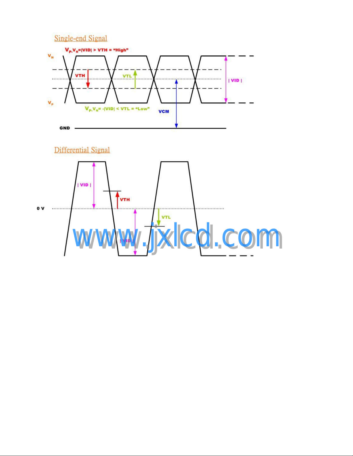
55..55 SSiiggnnaall EElleeccttrriiccaall CChhaarraacctteerriissttiiccss
Input signals shall be low or Hi-Z state when VDD is off. It is recommended to refer the specifications.
Differential input voltage
LVDS input common
mode voltage
Differential Input High
Threshold Voltage
Differential Input Low
Note: LVDS Signal Waveform
Item Symbol Min. Typ. Max. Unit
|VID|
VCM
VTH
VTL
0.1
1
-
-100
-
1.2 1.5
-
-
0.6
100
-
Condition
V
VTH/VTL=+-100mV
V
mV
VCM=1.2V
mV
www.jxlcd.com
www.jxlcd.com
(C) Copyright AU Optronics
May, 2005 All Rights Reserved. A121EW02 Vx
No Reproduction and Redistribution Allowed.
14/22
Page 15
www.jxlcd.com
www.jxlcd.com
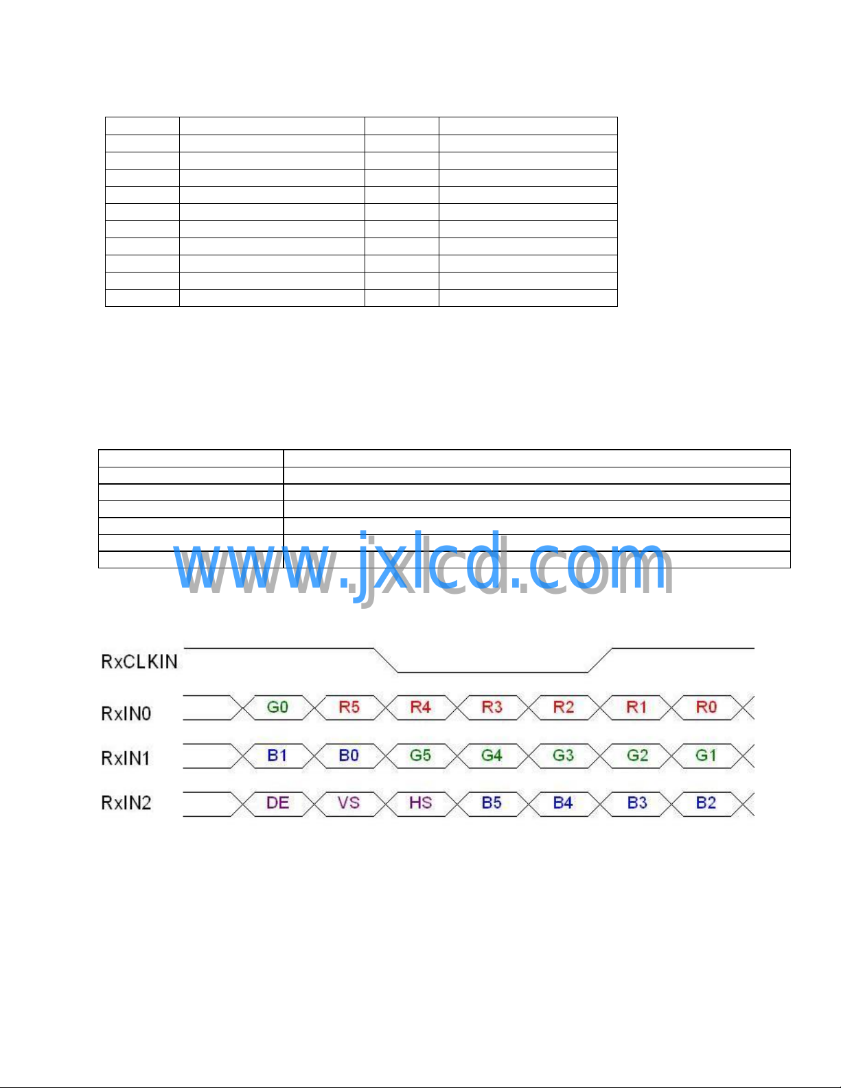
6.0 Pixel Format Image
Following figure shows the relationship of the input signals and LCD pixel format.
(C) Copyright AU Optronics
May, 2005 All Rights Reserved. A121EW02 Vx
No Reproduction and Redistribution Allowed.
15/22
Page 16

Parameter
Symbol
Min.
T
yp.
Max.
Unit
Clock f
requency
1/ T
Clock
62
68.9
75
MHz
Period
TV 803
816
832
Active
T
V
D
800
800
800
Blanking
T
V
B
3
16
32
H
D
Blanking
T
H
B
22
128
420
7.0 Timing Control
77..11 TTiimmiinngg CChhaarraacctteerriissttiiccss
This is the signal timing required at the input of the user connector. All of the interface signal timing should be
satisfied with the following specifications.
Note : DE mode only
www.jxlcd.com
www.jxlcd.com
Frame Rate
Vertical
Section
Period
Horizontal
Active
Section
TH
T
-
50
60
-
Hz
1302
-
1408
1280
1700
T
Line
-
T
Clock
77..22 TTiimmiinngg DDeeffiinniittiioonn
(C) Copyright AU Optronics
May, 2005 All Rights Reserved. A121EW02 Vx
No Reproduction and Redistribution Allowed.
16/22
Page 17

www.jxlcd.com
www.jxlcd.com
(C) Copyright AU Optronics
May, 2005 All Rights Reserved. A121EW02 Vx
No Reproduction and Redistribution Allowed.
17/22
Page 18

8.0 Power Consumption
Input power specifications are as follows;
Symbol Parameter Min Typ Max Units
Module
VDD Logic/LCD Drive
PDD VDD Power 1.6 [Watt] All Black Pattern
PDD Max VDD Power max 1.7 [Watt]
IDD IDD Current 400 mA 64 Grayscale Pattern
IDD Max IDD Current max 650 mA Vertical stripe line Pattern
VDDrp Allowable
VDDns Allowable
Note 1: VDD=3.3V
3.0 3.3 3.6 [Volt] Load Capacitance 20uF
Voltage
Max Pattern (Note 1)
(Note 1)
Logic/LCD Drive
Ripple Voltage
Logic/LCD Drive
Ripple Noise
500 [mV]
p-p
100 [mV]
p-p
Condition
www.jxlcd.com
www.jxlcd.com
(C) Copyright AU Optronics
May, 2005 All Rights Reserved. A121EW02 Vx
No Reproduction and Redistribution Allowed.
18/22
Page 19

Value
Min.
T
yp.
Max.
T6
200
-
-
(ms)
9.0 Power ON/OFF Sequence
VDD power and lamp on/off sequence is as follows. Interface signals are also shown in the chart.
Signals from any system shall be Hi-Z state or low level when VDD is off.
T1
90% 90%
10% 10%
Power Supply VDD
T2 T3 T4
LVDS Interface
VALID
T5 DATA T6
Backlight On
www.jxlcd.com
www.jxlcd.com
Power Sequence Timing
Parameter
T1
T2
T3
T4
T5
0.4
500
200
0
0
-
-
-
-
-
50
50
50
-
-
Units
(ms)
(ms)
(ms)
(ms)
(ms)
Note 1: T5, T6 is only for assuring the display quality. (T5,T6 spec may be ignored if don’t care the display quality.)
(C) Copyright AU Optronics
May, 2005 All Rights Reserved. A121EW02 Vx
No Reproduction and Redistribution Allowed.
19/22
Page 20

10.0 Reliability /Safety Requirement
RReelliiaabbiilliittyy TTeesstt CCoonnddiittiioonnss
No.
1 High temperature storage
2 Low temperature storage
3 High temperature operation
4 Low temperature operation
5 High temperature and high humidity
6 Thermal shock
Note1: Ta: Ambient temperature.
Note2: Tp: Center point temperature of Panel Surface.
Note3: All the cosmetic specification is judged before the reliability stress.
Test items Conditions Remark
Ta= 70℃
Ta= -20℃
Tp= 70℃
Ta= 0℃
Tp= 50℃, 80% RH
-20°C to +60°C, Ramp ≤20°C/min,
Duration at Temp. = 30min, Test Cycles =
240Hrs
240Hrs
240Hrs
240Hrs
240Hrs Operation
Non-operation
www.jxlcd.com
www.jxlcd.com
(C) Copyright AU Optronics
May, 2005 All Rights Reserved. A121EW02 Vx
No Reproduction and Redistribution Allowed.
20/22
Page 21

11. Outline Drawing
www.jxlcd.com
www.jxlcd.com
(C) Copyright AU Optronics
May, 2005 All Rights Reserved. A121EW02 Vx
No Reproduction and Redistribution Allowed.
21/22
Page 22

Packaging description
1122..
TBD
www.jxlcd.com
www.jxlcd.com
(C) Copyright AU Optronics
May, 2005 All Rights Reserved. A121EW02 Vx
No Reproduction and Redistribution Allowed.
22/22
 Loading...