

AUO T650QVJ02.0 Specification

T650QVJ02.0 Product Specification
Rev 1.0
Model Name: T650QVJ02.0
Issue Date : 2013/04/23
( )Preliminary Specifications
(****)Final Specifications
Customer Signature Date AUO Date
Approved By
_________________________________
Note
Approval By PM Director
CP Wang
____________________________________
Reviewed By RD Director
Eugene CC Chen
____________________________________
Reviewed By Project Leader
Stanley Lo
__________ __________________________
Prepared By PM
Mick Chen
____________________________________
© Copyright AUO Optronics Corp. 2009 All Rights Reserved. Page 1 / 38
Contents
T650QVJ02.0 Product Specification
Rev 1.0
No
CONTENTS
RECORD OF REVISIONS
1 GENERAL DESCRIPTION
2 ABSOLUTE MAXIMUM RATINGS
3 ELECTRICAL SPECIFICATION
3-1 ELECTRIACL CHARACTERISTICS
3-2 INTERFACE CONNECTIONS
3-3 SIGNAL TIMING SPECIFICATION
3-4 SIGNAL TIMING WAVEFORM
3-5 COLOR INPUT DATA REFERENCE
3-6 POWER SEQUENCE
3-7 BACKLIGHT SPECIFICATION
4 OPTICAL SPECIFICATION
5 MECHANICAL CHARACTERISTICS
6 RELIABILITY TEST ITEMS
7 INTERNATIONAL STANDARD
7-1 SAFETY
7-2 EMC
8 PACKING
8-1 DEFINITION OF LABEL
8-2 PACKING METHODS
8-3 PALLET AND SHIPMENT INFORMATION
9 PRECAUTION
9-1 MOUNTING PRECAUTIONS
9-2 OPERATING PRECAUTIONS
9-3 ELECTROSTATIC DISCHARGE CONTROL
9-4 PRECAUTIONS FOR STRONG LIGHT EXPOSURE
9-5 STORAGE
9-6 HANDLING PRECAUTIONS FOR PROTECT FILM
© Copyright AUO Optronics Corp. 2009 All Rights Reserved. Page 2 / 38

Record of Revision
T650QVJ02.0 Product Specification
Rev 1.0
Version
0.1 2013/01/14 First release
0.2 2013/01/29 7 Update Part 3 electrical spec
0.3 2013/01/29 20 Update LCD power connector
0.4 2013/01/30 31 Update mechanical drawing
0.5 2013/01/31 7 Update I2C spec
0.6 2013/01/31 7,11 Update DC characteristics & LVDS 51pin assignment
0.7 2013/02/07 11 Change 51pin; pin 7 function decription
0.8 2013/03/26 7 DC/AC characteristics
14 Timing spec
15,16 Timing waveform
18 Update Power sequence
23 Revise Color coordination spec
11 51pin, pin1 change
0.9 2013/04/12 11 51pin, pin3 change
1.0 2013/04/23 34 Revise safety information: E204358E204356
Date Page Description
© Copyright AUO Optronics Corp. 2009 All Rights Reserved. Page 3 / 38
T650QVJ02.0 Product Specification
Rev 1.0
1. General Description
This specification applies to the 65 inch Color TFT-LCD Module T650QVJ02.0. This LCD module has a TFT active
matrix type liquid crystal panel 3,840x2,160 pixels, and diagonal size of 65 inch. This module supports 3,840x2,160
mode. Each pixel is divided into Red, Green and Blue sub-pixels or dots which are arranged in vertical stripes. Gray
scale or the brightness of the sub-pixel color is determined with a 10-bit gray scale signal for each dot.
The T650QVJ02.0 has been designed to apply the 10-bit LVDS interface method. It is intended to support displays
where high brightness, wide viewing angle, high color saturation, and high color depth are very important. Also, 3D
function is also embedded into front glass as pattern retarder.
* General Information
Items Specification Unit Note
Active Screen Size 65 inch
Display Area 1428.48(H) x 803.52(V) mm
Outline Dimension 1454.3(H) x 831.5 (V) x 18(D) mm D: front bezel to back bezel
Driver Element a-Si TFT active matrix
Bezel Opening
Display Colors 10 bit, 16.7M Colors
Number of Pixels 3840x2160 Pixel
Pixel Pitch 0.372 (H) x 0.372(W) mm
Pixel Arrangement RGB vertical stripe
Display Operation Mode Normally Black
Rotate Function Unachievable Note 1
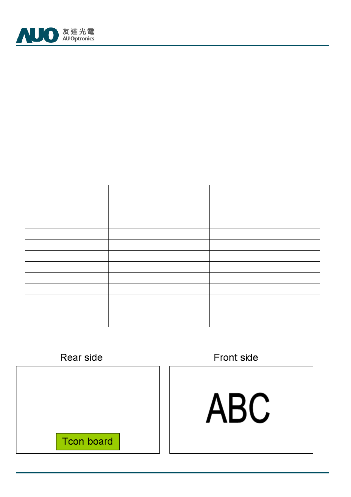
Display Orientation Signal input with “ABC” Note 2
Note 1: Rotate Function refers to LCD display could be able to rotate.
Note 2: LCD display as below illustrated when signal input with “ABC”.
1434.5 (H) x 809.6 (V)
mm
© Copyright AUO Optronics Corp. 2009 All Rights Reserved. Page 4 / 38

T650QVJ02.0 Product Specification
2. Absolute Maximum Ratings
The followings are maximum values which, if exceeded, may cause faulty operation or damage to the unit
Rev 1.0
Item Symbol
Logic/LCD Drive Voltage VDD -0.3 14 [Volt] Note 1
Input Voltage of Signal Vin -0.3 4 [Volt] Note 1
Operating Temperature TOP 0 +50 [oC] Note 2
Operating Humidity HOP 10 90 [%RH] Note 2
Storage Temperature TST -20 +60 [oC] Note 2
Storage Humidity HST 10 90 [%RH] Note 2
Panel Surface Temperature PST 65 [oC] Note 3
Note 1: Duration:50 msec.
Note 2 : Maximum Wet-Bulb should be 39 and No condensation.℃
The relative humidity must not exceed 90% non-condensing at temperatures of 40 or less. At temperatures greater
than 40 , the wet bulb temperature must not exceed 39 .
Note 3: Surface temperature is measured at 50℃ Dry condition
℃ ℃
Min Max Unit Conditions
℃
© Copyright AUO Optronics Corp. 2009 All Rights Reserved. Page 5 / 38

T650QVJ02.0 Product Specification
Rev 1.0
3. Electrical Specification
The T650QVJ02.0 requires two power inputs. One is employed to power the LCD electronics and to drive the TFT array
and liquid crystal. The other is to power Back Light Unit.
3.0 ASIC feature
Input resolution FHD120Hz / UHD 30Hz/ 4k1k 30Hz switchable
MEMC Function with High/Middle/Low level
2D / 3D switchable
Video Mute Function
OSD protection function
© Copyright AUO Optronics Corp. 2009 All Rights Reserved. Page 6 / 38
3.1 Electrical Characteristics
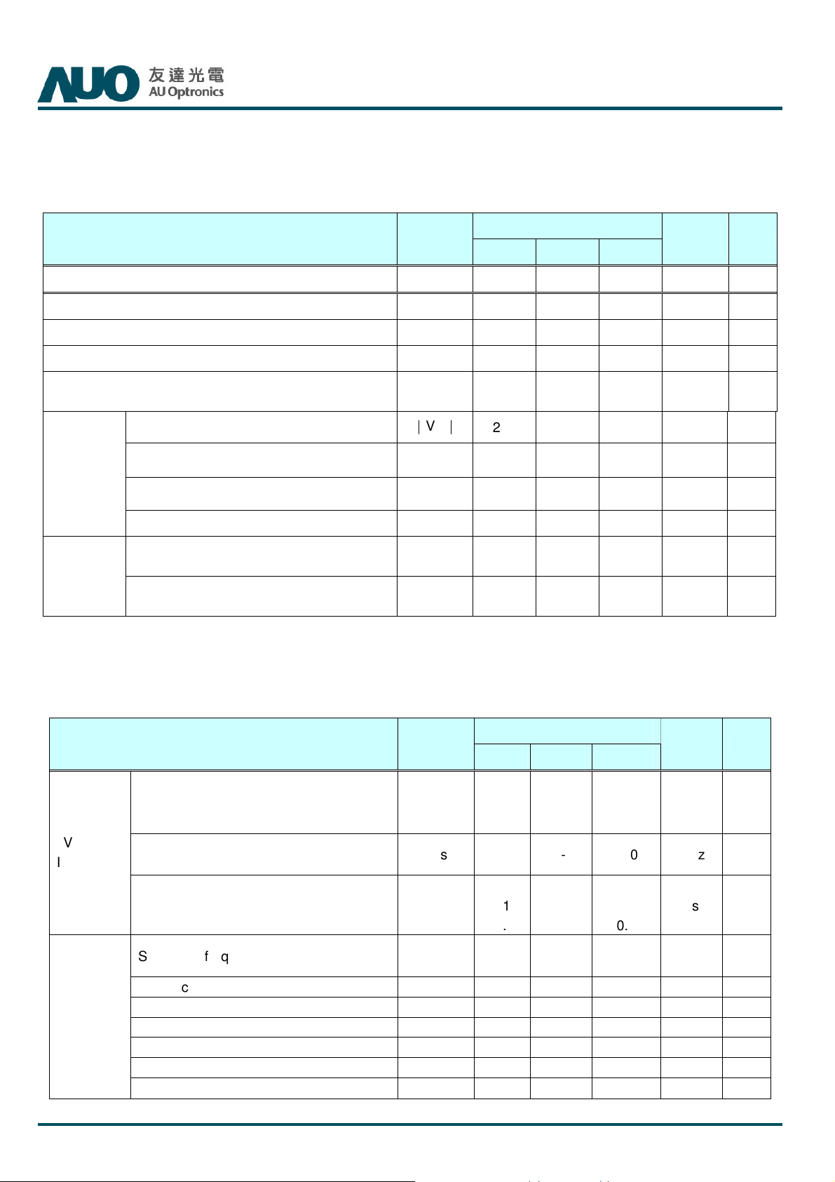
3.1.1: DC Characteristics
T650QVJ02.0 Product Specification
Rev 1.0
Parameter Symbol
Unit Note
Min. Typ. Max
LCD
Power Supply Input Voltage (for input power=12V) VDD 10.8 12 13.2 VDC
Power Supply Input Current (Define to section:1.1) IDD -- 1.8 3.7 A 1
Value
Inrush Current (Define to section:1.1) I
Permissible Ripple of Power Supply Input Voltage
(for input power=12V)
Input Differential Voltage
LVDS
Interface
Differential Input High Threshold Voltage VTH +100 -- +300 mVDC 4
Differential Input Low Threshold Voltage VTL -300 -- -100 mVDC 4
Input Common Mode Voltage V
CMOS
Interface
Input High Threshold Voltage
Input Low Threshold Voltage
-- -- 5 A 2
RUSH
VRP -- --
∣
V
∣
ID
1.1 1.25 1.4 VDC 4
ICM
VIH
(High)
VIL
(Low)
200 400 600 mVDC 4
2.0 -- 3.3 VDC 5
0 -- 0.8 VDC 5
VDD *
5%
mV
pk-pk
3
3.1.2: AC Characteristics
Parameter Symbol
Receiver Clock : Spread Spectrum
Modulation range
LVDS
Interface
Receiver Clock : Spread Spectrum
Modulation frequency
Receiver Data Input Margin
Fclk = 150 MHz
Fclk = 85 MHz
SCL clock frequency F
I2C clock high level T
I2C
Interface
I2C clock low level T
I2C data setup time T
I2C data hold time T
SDA and SCL rise time TR -- -- 0.3 us
SDA and SCL fall time TF -- -- 0.3 us
Value
Unit Note
Min. Typ. Max
Fclk_ss
Fss
tRMG
SCL
SCHi
SCLo
SDS
SDH
Fclk
-3%
50
-0.15
-0.4
-- --
--
--
--
--
0.6 -- -- us
1.3 -- -- us
0.1 -- -- us
0 -- 900 us
Fclk
+3%
200
MHz 6
KHz
0.15
0.4
ns
400 KHZ
6
7
© Copyright AUO Optronics Corp. 2009 All Rights Reserved. Page 7 / 38
3.1.3: Driver Characteristics
s
µ
Item Symbol Min Max Unit condition
T650QVJ02.0 Product Specification
Rev 1.0
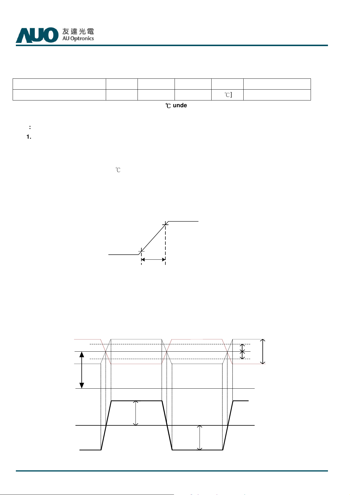
Driver Surface Temperature DST 100
Any point on the driver surface must be less than 100
℃℃℃℃
under any condition
Note:
1. Test Condition:
(1) V
(2) Fv = Type Timing 120Hz
(3) Fclk= Max freq.
(4) Temperature = 25 ℃
(5) Typ. Input current : White Pattern
>> refer to “Section:3.3 Signal Timing Specification, Typical timing”
2. Measurement condition : Rising time = 400us
= 12.0V
DD
Max. Input current: Heavy loading pattern defined by AUO
90%
GND
GND
GNDGND
10%
[℃]
Note
VVVV
DD
DD
DDDD
3. Test Condition:
(1) The measure point of V
(2) Under Max. Input current spec. condition.
4. V
= 1.25V
ICM
L V D S -
V
IC M
L V D S +
G N D
0 V
is in LCM side after connecting the System Board and LCM.
RP
400
400
400400
|VID|
V
T H
|VID|
V
T L
|VID|
© Copyright AUO Optronics Corp. 2009 All Rights Reserved. Page 8 / 38
T650QVJ02.0 Product Specification
5. The measure points of V
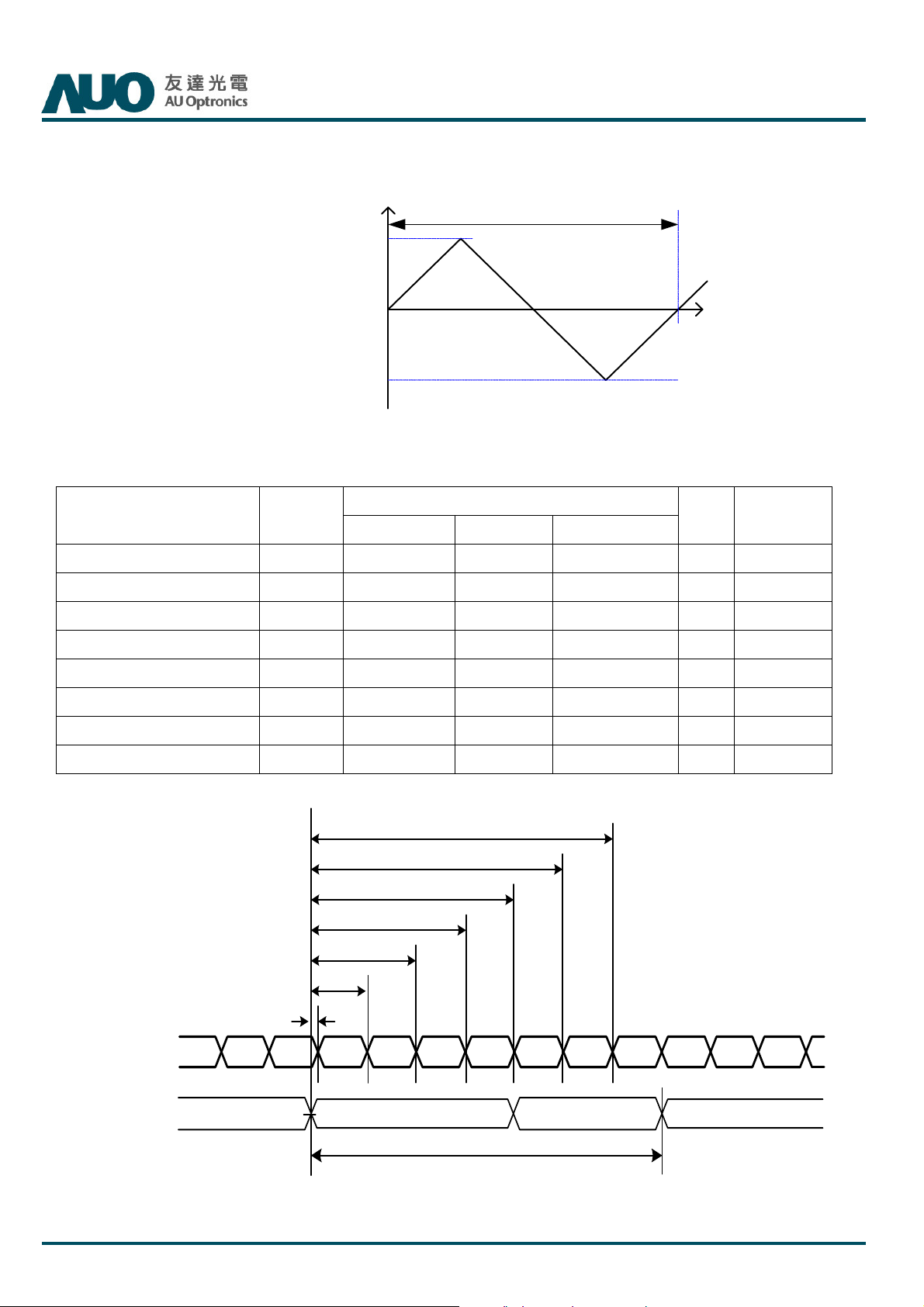
6. LVDS Receiver Clock SSCG (Spread spectrum clock generator) is defined as below figures.
7. Receiver Data Input Margin
and V
IH
Fclk
Fclk____ss
FclkFclk
ss((((max
ssss
Fclk
Fclk
FclkFclk
Fclk
Fclk____ss
FclkFclk
ss((((min
ssss
are in LCM side after connecting the System Board and LCM.
IL
1111////FFFF
SS
SS
SSSS
max))))
maxmax
min))))
minmin
Rev 1.0
Parameter Symbol
Min Type Max
Input Clock Frequency Fclk Fclk (min) -- Fclk (max) MHz
Input Data Position0 tRIP1 -|tRMG| 0 |tRMG| ns
Input Data Position1 tRIP0 T/7-|tRMG| T/7 T/7+|tRMG| ns
Input Data Position2 tRIP6 2T/7-|tRMG|
Input Data Position3 tRIP5 3T/7-|tRMG|
Input Data Position4 tRIP4 4T/7-|tRMG|
Input Data Position5 tRIP3 5T/7-|tRMG|
Input Data Position6 tRIP2 6T/7-|tRMG|
Rating
Unit
2T/7 2T/7+|tRMG| ns
3T/7 3T/7+|tRMG| ns
4T/7 4T/7+|tRMG| ns
5T/7 5T/7+|tRMG| ns
6T/7 6T/7+|tRMG| ns
tRIP2
tRIP3
tRIP4
tRIP5
Note
T=1/Fclk
tRIP6
tRIP0
tRIP1
LVDS-Rx
Input Data
Rx1 Rx0 Rx6 Rx5 Rx4 Rx3 Rx2 Rx1 Rx0 Rx6Rx2Rx3
LVDS-Rx
VVVV
=
= 0000VVVV
= =
diff
diff
Input Clock
diff diff
1/Fclk=T
© Copyright AUO Optronics Corp. 2009 All Rights Reserved. Page 9 / 38
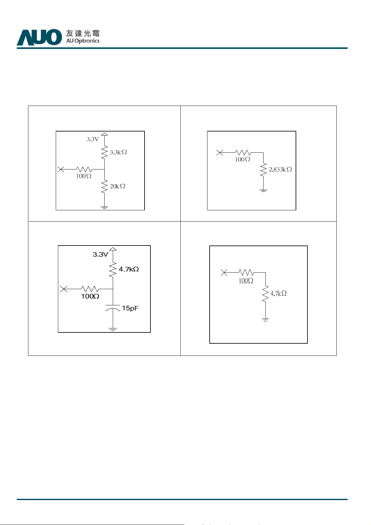
3.2 Interface Connections
3.2.1: LVDS connector control and I2C pin description
T650QVJ02.0 Product Specification
Rev 1.0
Note * : Open/High(3.3V)
Note **** : SCL/SDA
Note ** : Open/Low(GND)
Note ***** : WP
© Copyright AUO Optronics Corp. 2009 All Rights Reserved. Page 10 / 38
3.2.2: LVDS Pin-Assignment
LCD connector: 187059-51221-1 (JAE, LVDS connector)
T650QVJ02.0 Product Specification
Rev 1.0
187060-41221-1 (JAE, LVDS connector)
Mating connector:
PIN
1
2
3
4
5
6
7
8
9
10
11
12
13
14
15
16
17
18
19 CH1_CLK- LVDS Channel 1, Clock - 44
20 CH1_CLK+ LVDS Channel 1, Clock + 45
21
22
23
24
25
Symbol Description PIN
N.C AUO Internal Use Only 26
SCL I2C Serial Clock 27
N.C AUO Internal Use Only 28
SDA I2C Serial Data 29
N.C AUO Internal Use Only 30
N.C AUO Internal Use Only 31
SELLVDS
N.C AUO Internal Use Only 33
N.C AUO Internal Use Only 34
N.C AUO Internal Use Only 35
GND Ground 36 CH2_CLK+ LVDS Channel 2, Clock +
CH1_0- LVDS Channel 1, Signal 0- 37
CH1_0+ LVDS Channel 1, Signal 0+ 38
CH1_1- LVDS Channel 1, Signal 1- 39
CH1_1+ LVDS Channel 1, Signal 1+ 40
CH1_2- LVDS Channel 1, Signal 2- 41
CH1_2+ LVDS Channel 1, Signal 2+ 42
GND Ground 43
GND Ground 46
CH1_3- LVDS Channel 1, Signal 3- 47
CH1_3+ LVDS Channel 1, Signal 3+ 48
CH1_4- LVDS Channel 1, Signal 4- 49
CH1_4+ LVDS Channel 1, Signal 4+ 50
LVDS Format Select
Open/High(3.3V) for JEIDA,
Low(GND) for NS
51
32
Symbol Description
GND Ground
GND Ground
CH2_0- LVDS Channel 2, Signal 0-
CH2_0+ LVDS Channel 2, Signal 0+
CH2_1- LVDS Channel 2, Signal 1-
CH2_1+ LVDS Channel 2, Signal 1+
CH2_2- LVDS Channel 2, Signal 2-
CH2_2+ LVDS Channel 2, Signal 2+
GND Ground
CH2_CLK- LVDS Channel 2, Clock -
GND Ground
CH2_3- LVDS Channel 2, Signal 3-
CH2_3+ LVDS Channel 2, Signal 3+
CH2_4- LVDS Channel 2, Signal 4-
CH2_4+ LVDS Channel 2, Signal 4+
GND Ground
GND Ground
GND Ground
GND Ground
N.C.
N.C.
N.C.
N.C.
N.C.
N.C AUO Internal Use Only
No connection (for AUO test only.
Do not connect)
No connection (for AUO test only.
Do not connect)
No connection (for AUO test only.
Do not connect)
No connection (for AUO test only.
Do not connect)
No connection (for AUO test only.
Do not connect)
Note: N.C. : please leave this pin unoccupied. It can not be connected by any signal (Low/GND/High).
© Copyright AUO Optronics Corp. 2009 All Rights Reserved. Page 11 / 38
T650QVJ02.0 Product Specification
No connection (for AUO test only. Do
Do
No connection (for AUO test only. Do
No connection (for AUO test only. Do
. Do
No connection (for AUO test only. Do
No connection (for AUO test only. Do
only. Do
Rev 1.0
PIN Symbol Description PIN
1
2
3
4
5
6
7
8
9
10 CH3_0- LVDS Channel 3, Signal 0- 30
11 CH3_0+
12 CH3_1- LVDS Channel 3, Signal 1- 32
13 CH3_1+
14 CH3_2- LVDS Channel 3, Signal 2- 34 CH4_CLK+ LVDS Channel 4, Clock +
15 CH3_2+
16
17 CH3_CLK18 CH3_CLK+
19
20 CH3_3- LVDS Channel 3, Signal 3- 40
N.C.
N.C.
N.C.
N.C.
N.C.
N.C.
N.C.
N.C.
GND Ground 29
GND Ground 36
GND Ground 39
No connection (for AUO test only.
No connection (for AUO test only
No connection (for AUO test
LVDS Channel 3, Signal 0+ 31
LVDS Channel 3, Signal 1+ 33 CH4_CLK- LVDS Channel 4, Clock -
LVDS Channel 3, Signal 2+ 35
not connect)
not connect)
not connect)
not connect)
not connect)
not connect)
not connect)
not connect)
LVDS Channel 3, Clock - 37
LVDS Channel 3, Clock + 38
41
21
22
23
24
25
26
27
28
Symbol Description
CH3_3+ LVDS Channel 3, Signal 3+
CH3_4- LVDS Channel 3,Signal 4-
CH3_4+ LVDS Channel 3,Signal 4+
GND Ground
GND Ground
CH4_0- LVDS Channel 4, Signal 0-
CH4_0+ LVDS Channel 4, Signal 0+
CH4_1- LVDS Channel 4, Signal 1-
CH4_1+ LVDS Channel 4, Signal 1+
CH4_2- LVDS Channel 4, Signal 2-
CH4_2+ LVDS Channel 4, Signal 2+
GND Ground
GND Ground
CH4_3- LVDS Channel 4, Signal 3-
CH4_3+ LVDS Channel 4, Signal 3+
CH4_4- LVDS Channel 4,Signal 4-
CH4_4+ LVDS Channel 4,Signal 4+
GND Ground
GND Ground
Note: N.C. : please leave this pin unoccupied. It can not be connected by any signal (Low/GND/High).
PI
N
1
2
3
4
5
6
7
8
9
10
11
12
LCD Power connector:
Power CN(12pin):MSAK242151P12R (STM)
Symbol Description
PWR Power 12V IN PWR Power 12V IN
PWR Power 12V IN PWR Power 12V IN
PWR Power 12V IN PWR Power 12V IN
PWR Power 12V IN PWR Power 12V IN
PWR Power 12V IN PWR Power 12V IN
NC NC Pin
NC NC Pin
GND Ground
GND Ground
GND Ground
GND Ground
GND Ground
© Copyright AUO Optronics Corp. 2009 All Rights Reserved. Page 12 / 38
 Loading...