

AUO T650QVD01.0 Specification
T650QVD01.0 Product Specification
__________________________
Rev 0.6
Model Name: T650QVD01.0
Issue Date : 2013/04/08
( )Preliminary Specifications
(****)Final Specifications
Customer Signature Date AUO Date
Approved By
_________________________________
Note
Approval By PM Director
CP Wang
Reviewed By RD Director
Eugene CC Chen
____________________________________
Reviewed By Project Leader
Stone Shih
____________________________________
Prepared By PM
__________
Mick Chen
____________________________________

T650QVD01.0 Product Specification
Rev 0.6
CONTENTS
CONTENTS ................................................................................................................................................................2
RECORD OF REVISION ............................................................................................................................................3
1. GENERAL DESCRIPTION ................................................................................................................................4
2. ABSOLUTE MAXIMUM RATINGS.....................................................................................................................5
3. ELECTRICAL SPECIFICATION.........................................................................................................................6
3.1 ELECTRICAL CHARACTERISTICS .........................................................................................................6
3.1.1 DC CHARACTERISTICS ......................................................................................................................6
3.1.2 AC CHARACTERISTICS ......................................................................................................................7
3.2 INTERFACE CONNECTIONS.................................................................................................................10
3.2.1 T-CON BOARD PIN MAP ...................................................................................................................10
3.3 SIGNAL TIMING SPECIFICATION .........................................................................................................14
3.4 SIGNAL TIMING WAVEFORMS..............................................................................................................14
3.5 COLOR INPUT DATA REFERENCE.......................................................................................................15
3.6 POWER SEQUENCE FOR LCD .............................................................................................................17
3.7 VCOM ADJUST SOP ..............................................................................................................................19
3.7.1 VCOM I2C TUNING STEP..................................................................................................................19
3.7.2 FLICKER PATTERN............................................................................................................................19
3.7.3 WP (WRITE PROTECT) DISABLE .....................................................................................................19
3.7.4 ADJUST SOP......................................................................................................................................19
3.7.5 INTERVAL OF STEP TO STEP ..........................................................................................................20
4. OPTICAL SPECIFICATION..............................................................................................................................21
5. MECHANICAL CHARACTERISTICS...............................................................................................................27
6. PACKING .........................................................................................................................................................28
7. PRECAUTIONS ...............................................................................................................................................31
7.1 MOUNTING PRECAUTIONS ..................................................................................................................31
7.2 OPERATING PRECAUTIONS ................................................................................................................31
7.3 ELECTROSTATIC DISCHARGE CONTROL ..........................................................................................31
7.4 PRECAUTIONS FOR STRON LIGHT EXPOSURE ...............................................................................32
7.5 STORAGE ...............................................................................................................................................32
7.6 HANDLING PRECAUTIONS FOR PROTECTION FILM OF POLARIZER.............................................32
2

RECORD OF REVISION
T650QVD01.0 Product Specification
Rev 0.6
Version
0.0 2012/10/19 First release
0.1 2012/12/14 6 Revise Tr% and update 3.1.1
0.2 2012/12/15 6 Update No. 3 Electrical spec
0.3 2012/12/21 27 Revise No. 6 Packing spec
0.4 2013/02/27 6
0.4
0.4
0.4
0.4
0.4
0.4
0.4
0.4
0.4
Date Page Description
Power Supply Input Current:3.71→ 4A
2013/02/27 6
2013/02/27 6 Delete Input Differential Voltage
2013/02/27 6
2013/02/27 6
2013/02/27 7 Add Inter-block skew
2013/02/27 11
2013/02/27 12
2013/02/27 16 Update 3.5 COLOR INPUT DATA REFERENCE
2013/02/27 33 Update EDID data
Inrush Current:5A → 8.2A
Power Consumption typ.:13.99 → typ. 12.72
Power Consumption max.:44.52 → max. 63.36
Add Power CN(12pin):SM12B-PAHS-TBT(JST)
Add FFC Connector (80 Pin):196225-80041(P-two) / 106C80-100000-
G2-R(CHIEF LAND)
0.4
2013/02/27 27 T-con board drawing add
0.5 2013/03/04 28 Revise carton label information and drawing
0.6 2013/04/08 10 Revise 51 pin no. 8 function
3
T650QVD01.0 Product Specification
Rev 0.6
1. GENERAL DESCRIPTION
This specification applies to the 65 inch Color TFT-LCD SKD model T650QVD01.0. This LCD Open Cell Unit
has a TFT active matrix type liquid crystal panel 3840x2160 pixels, and diagonal size of 65 inch. This Open Cell
Unit supports 3840x2160 mode. Each pixel is divided into Red, Green and Blue sub-pixels or dots which are
arranged in vertical stripes. Gray scale or the brightness of the sub-pixel color is determined with a 10-bit gray
scale signal for each dot.
* General Information
Items Specification Unit Note
Active Screen Size 65 inch
Display Area 1428.48(H) x 803.52(V) mm
Outline Dimension 1444.08(H) x 821.12 (V) x 2.26(D) mm D: cell thickness
Driver Element a-Si TFT active matrix
Bezel Opening 1434.5 (H) x 809.6 (V) mm Recommend
Display Colors 10 bit, 16.7M Colors
Number of Pixels 3840x2160 Pixel
Pixel Pitch 0.372 (H) x 0.372(W) mm
Pixel Arrangement RGB vertical stripe
Display Operation Mode Normally Black
Surface Treatment Anti-Glare, 3H Haze=2%
Weight 4.7 kg
Rotate Function Achievable or Unachievable Note 1
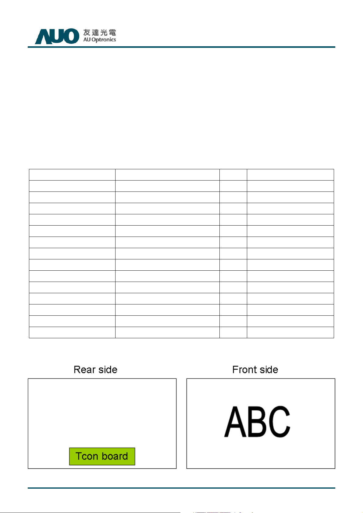
Display Orientation Signal input with “ABC” Note 2
Note 1: Rotate Function refers to LCD display could be able to rotate.
Note 2: LCD display as below illustrated when signal input with “ABC”.
4
T650QVD01.0 Product Specification
Rev 0.6
2. ABSOLUTE MAXIMUM RATINGS
The followings are maximum values which, if exceeded, may cause faulty operation or damage to the unit
Item Symbol Min Max Unit Conditions
Logic/LCD Drive Voltage Vcc -0.3 14 [Volt] Note 1
Input Voltage of Signal Vin -0.3 3.6 [Volt] Note 1
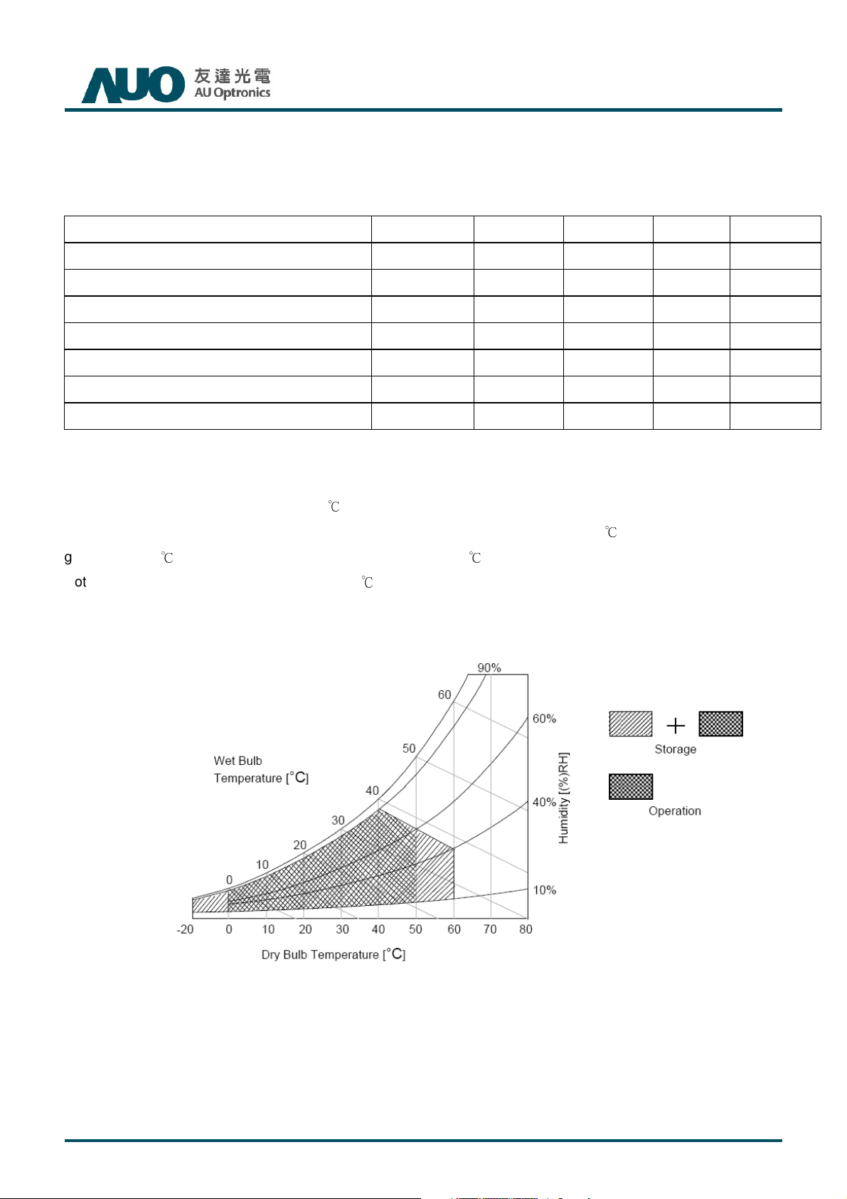
Operating Temperature TOP 0 +50 [oC] Note 2
Operating Humidity HOP 10 90 [%RH] Note 2
Storage Temperature TST -20 +60 [oC] Note 2
Storage Humidity HST 10 90 [%RH] Note 2
Panel Surface Temperature PST 65 [oC] Note 3
Note 1: Duration:50 msec.
Note 2 : Maximum Wet-Bulb should be 39 and No condensation.℃
The relative humidity must not exceed 90% non-condensing at temperatures of 40 or less. At temperatures℃
greater than 40 , the wet bulb temperature must not exceed 39 .
Note 3: Surface temperature is measured at 50℃ Dry condition
℃ ℃
5
T650QVD01.0 Product Specification
Rev 0.6
3. ELECTRICAL SPECIFICATION
The T650QVD01.0 Open Cell Unit requires power input which is employed to power the LCD electronics and to
drive the TFT array and liquid crystal.
3.1 ELECTRICAL CHARACTERISTICS
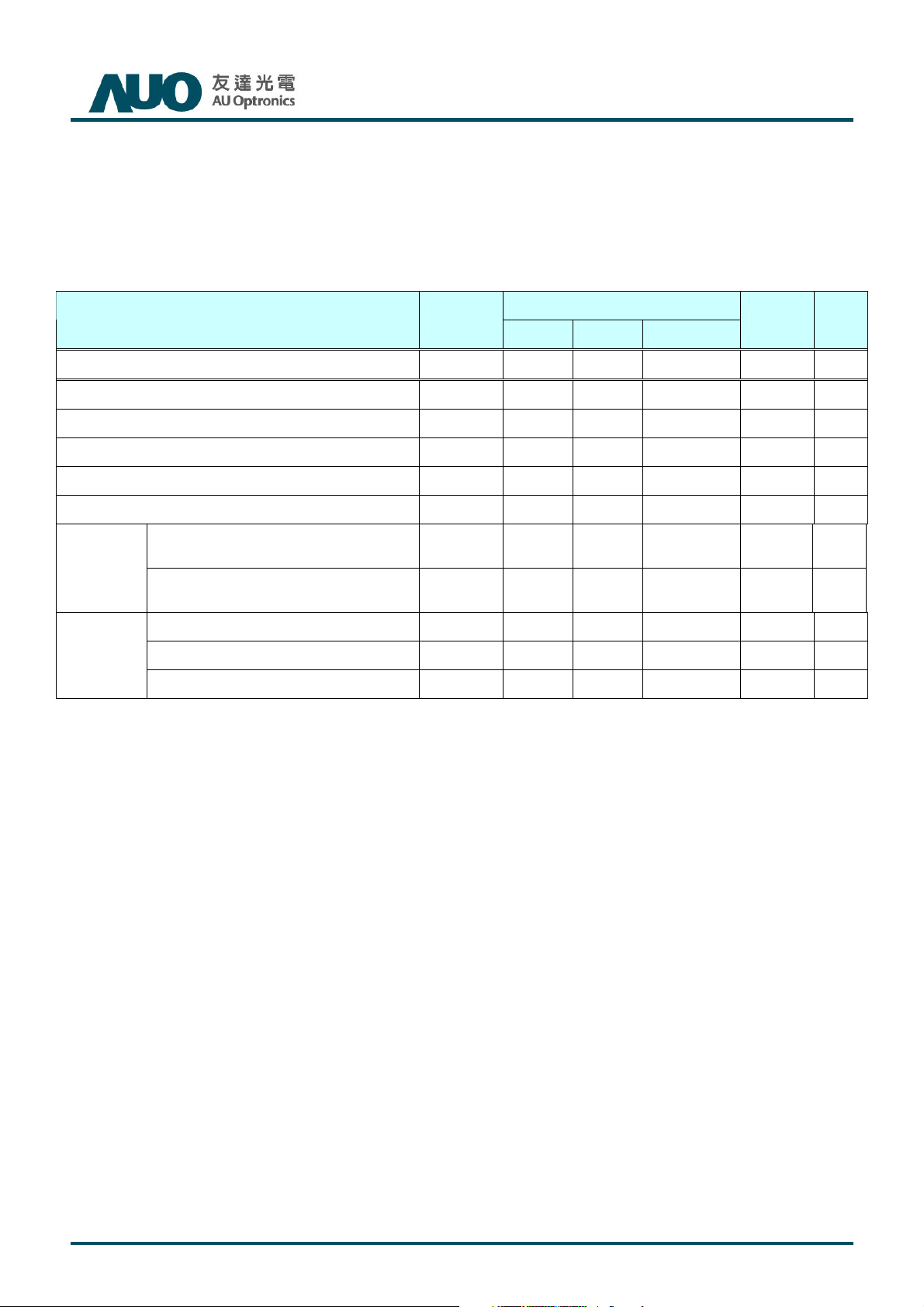
3.1.1 DC CHARACTERISTICS
Parameter Symbol
LCD
Power Supply Input Voltage VDD 10.8 12 13.2 VDC
Power Supply Input Current IDD -- 1.06 4 A 1
Power Consumption PC -- 12.72 63.36 Watt 1
Inrush Current I
Permissible Ripple of Power Supply Input Voltage
CMOS
Interface
V-by-one
Interface
Input High Threshold Voltage
Input Low Threshold Voltage
CML Differential Input High Threshold
CML Differential Input Low Threshold
CML Common mode Bias Voltage V
Value
Min. Typ. Max
-- -- 8.2 A 2
RUSH
VRP -- -- VDD * 5% mV
VIH
(High)
VIL
(Low)
V
+50 -- -- mVDC
RTH
V
-- -- -50 mVDC
RTL
0.8 0.9 1.0 mVDC
RCT
2.7 -- 3.3 VDC 4
0 -- 0.6 VDC 4
Unit Note
pk-pk
3
6
3.1.2: AC Characteristics
T650QVD01.0 Product Specification
Rev 0.6
V-by-one
Interface
I2C
Interface
Parameter Symbol
Unit Note
Min. Typ. Max
Value
8bit
10bit
8bit
10bit
VRXINP/N input each bit Period
CDR lock time(CDR training) T
ALN Training T
PDX active to hot plug enable T
Intra-pair skew T
Inter-pair skew T
Inter-block skew T
INTER_BLK
SCL clock frequency F
I2C clock high level T
I2C clock low level T
I2C data setup time T
I2C data hold time T
T
RRIP
(UI)
RLCK0
413
310
-- -- 1.0 ms 5
-- 30720
RALN
-- 40960
-- -- 1.0 us 5
RHPD0
-- -- 0.3 UI 6
INTRA
-- -- 5 UI 7
INTER
--
--
505 ps
379 ps
-- UI
-- UI
-- -- 0.5 DE 8
0 -- 400 KHZ
SCL
0.6 -- -- us
SCHi
1.2 -- -- us
SCLo
100 -- -- ns
SDS
0 -- 900 ns
SDH
SDA and SCL rise time TR -- -- 1000 ns
SDA and SCL fall time TF -- -- 300 ns
5
5
5
5
3.1.3: Driver Characteristics
Item Symbol Min Max Unit condition
Driver Surface Temperature DST 100
Note : Any point on the driver surface must be less than 100
[℃]
℃℃℃℃ under any conditions.
under any conditions.
under any conditions. under any conditions.
Note
7
Note :
s
µ
1. Test Condition:
(1) V
= 12.0V
DD
(2) Fv = Type Timing, 60Hz, 120Hz or Other
(3) Fclk= Max freq.
(4) Temperature = 25 ℃
(5) Typ. Input current : White Pattern
Max. Input current: Heavy loading pattern defined by AUO
>> refer to “Section:3.3 Signal Timing Specification, Typical timing”
2. Measurement condition : Rising time = 400us
90%
T650QVD01.0 Product Specification
Rev 0.6
VVVV
DD
DD
DDDD
GND
GND
GNDGND
10%
3. Test Condition:
(1) The measure point of V
is in LCM side after connecting the System Board and LCM.
RP
(2) Under Max. Input current spec. condition.
4. The measure points of V
and V
IH
are in LCM side after connecting the System Board and LCM.
IL
5. V-by-one Receiver start up timing waveform
400
400
400400
6. V-by-one Intra-pair Skew
7. V-by-one Inter-pair Skew
© Copyright AUO Optronics Corp. 2012 All Rights Reserved. Page 8 / 33
8. V-by-one Inter-block Skew
T650QVD01.0 Product Specification
Rev 0.6
© Copyright AUO Optronics Corp. 2012 All Rights Reserved. Page 9 / 33
3.2 INTERFACE CONNECTIONS
3.2.1 T-CON BOARD PIN MAP
●
LCD connector: FI-RE51S-HF (JAE, V-by-One 51pin connector)
T650QVD01.0 Product Specification
Rev 0.6
PIN
1
2
3
4
5
6
7
8
9
10
11
12
13
14
15
Symbol Description PIN
NC
NC
NC
NC
NC
NC
NC
NC
NC
NC
GND
GND
GND
GND
GND
AUO Internal Use Only
AUO Internal Use Only
AUO Internal Use Only
AUO Internal Use Only
AUO Internal Use Only
AUO Internal Use Only
AUO Internal Use Only
AUO Internal Use Only
AUO Internal Use Only
AUO Internal Use Only
Ground
Ground
Ground
Ground
Ground
26
27
28
29
30
31
32
33
34
35
36
37
38
39
40
Symbol Description
GND
Rx2n
Rx2p
GND
GND
Rx3n
Rx3p
GND
GND
Rx4n
Rx4p
GND
GND
Rx5n
Rx5p
CML Ground
V-by-One HS Data Lane 2
V-by-One HS Data Lane 2
CML Ground
CML Ground
V-by-One HS Data Lane 3
V-by-One HS Data Lane 3
CML Ground
CML Ground
V-by-One HS Data Lane 4
V-by-One HS Data Lane 4
CML Ground
CML Ground
V-by-One HS Data Lane 5
V-by-One HS Data Lane 5
16
17
18
19
20
21
22
23
24
25
HTPDN
LOCKN
Hot plug detect
GND
Rx0n
Rx0p
GND
GND
Rx1n
Rx1p
GND
CML Ground
V-by-One HS Data Lane 0
V-by-One HS Data Lane 0
CML Ground
CML Ground
V-by-One HS Data Lane 1
V-by-One HS Data Lane 1
CML Ground
Lock detect
41
42
43
44
45
46
47
48
49
50
51
GND
GND
Rx6n
Rx6p
GND
GND
Rx7n
Rx7p
GND
NC
NC
CML Ground
CML Ground
V-by-One HS Data Lane 6
V-by-One HS Data Lane 6
CML Ground
CML Ground
V-by-One HS Data Lane 7
V-by-One HS Data Lane 7
CML Ground
AUO Internal Use Only
AUO Internal Use Only
© Copyright AUO Optronics Corp. 2010 All Rights Reserved. Page 10 / 33
 Loading...