

AUO T645HW04.1 Specification
Model Name: T645HW04.1 SKD
Issue Date : 2013/6/14
(****)Preliminary Specifications
( )Final Specifications
Customer Signature Date AUO Date
Approved By
_________________________________
Note
Approval By PM Director
CP Wang
Reviewed By RD Director
Eugene CC Chen
Reviewed By Project Leader
Sun Wei Liang
Prepared By PM
Fanfan Lee
Contents
No
CONTENTS
RECORD OF REVISIONS
1 GENERAL DESCRIPTION
2 ABSOLUTE MAXIMUM RATINGS
3 ELECTRICAL SPECIFICATION
3-1 ELECTRIACL CHARACTERISTICS
3-2 INTERFACE CONNECTIONS
3-3 SIGNAL TIMING SPECIFICATION
3-4 SIGNAL TIMING WAVEFORM
3-5 COLOR INPUT DATA REFERENCE
3-6 POWER SEQUENCE
4 OPTICAL SPECIFICATION
5 OPEN CELL DRAWING
6 RELIABILITY TEST ITEMS
7 PACKING
7-1 DEFINITION OF LABEL
7-2 PACKING METHODS
7-3 PALLET AND SHIPMENT INFORMATION
8 PRECAUTION
8-1 MOUNTING PRECAUTIONS
8-2 OPERATING PRECAUTIONS
8-3 ELECTROSTATIC DISCHARGE CONTROL
8-4 PRECAUTIONS FOR STRONG LIGHT EXPOSURE
8-5 STORAGE
8-6 HANDLING PRECAUTIONS FOR PROTECT FILM

Record of Revision
Version
0.0 2013/06/14 First release
Date Page Description
1. General Description
This specification applies to the 65.0 inch Color TFT-LCD Module T645HW04 V1. This LCD module has a TFT
active matrix type liquid crystal panel 1,920x1,080 pixels, and diagonal size of 65.0 inch. This module supports
1,920x1,080 mode. Each pixel is divided into Red, Green and Blue sub-pixels or dots which are arranged in vertical
stripes. Gray scale or the brightness of the sub-pixel color is determined with a 8-bit gray scale signal for each dot.
The T645HW04 V1 has been designed to apply the 8-bit 2 channel LVDS interface method. It is intended to
support displays where high brightness, wide viewing angle, high color saturation, and high color depth are very
important.
* General Information
Items Specification Unit Note
Active Screen Size 65.00 inch
Display Area 1428.48 (H) x 803.52 (V) mm
Outline Dimension 1461.98 (H) x 839.24 (V) mm
Driver Element a-Si TFT active matrix
Display Colors 8 bit, 1073.7M Colors
Number of Pixels 1,920x1,080 Pixel
Pixel Pitch 0.744 (H) x 0.744 (W) mm
Pixel Arrangement RGB vertical stripe
Display Operation Mode Normally Black
Surface Treatment SC
Rotate Function Unachievable Note 1
Note 1: Rotate Function refers to LCD display could be able to rotate.
2. Absolute Maximum Ratings
The followings are maximum values which, if exceeded, may cause faulty operation or damage to the unit
Item Symbol Min Max Unit Conditions
Logic/LCD Drive Voltage VDD -0.3 14 [Volt] Note 1
Input Voltage of Signal Vin -0.3 4 [Volt] Note 1
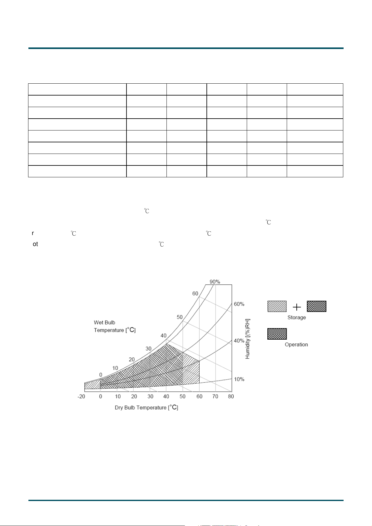
Operating Temperature TOP 0 +50 [oC] Note 2
Operating Humidity HOP 10 90 [%RH] Note 2
Storage Temperature TST -20 +60 [oC] Note 2
Storage Humidity HST 10 90 [%RH] Note 2
Panel Surface Temperature PST 65 [oC] Note 3
Note 1: Duration:50 msec.
Note 2 : Maximum Wet-Bulb should be 39 and No condensation.℃
The relative humidity must not exceed 90% non-condensing at temperatures of 40 or less. At temperatures
greater than 40 , the wet bulb temperature must not exceed 39 .
Note 3: Surface temperature is measured at 50℃ Dry condition
℃ ℃
℃
3. Electrical Specification
The T645HW04 V1 requires two power inputs. One is employed to power the LCD electronics and to drive the TFT
array and liquid crystal. The other is to power back light unit.
3.1 Electrical Characteristics
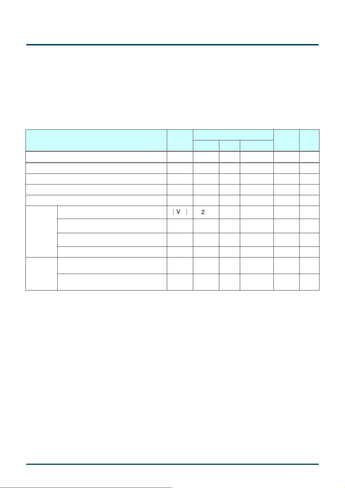
3.1.1: DC Characteristics
Parameter Symbol
Min. Typ.
Max
Unit Note
LCD
Power Supply Input Voltage VDD 10.8 12 13.2 VDC
Value
Power Supply Input Current IDD -- 0.61
Inrush Current I
-- -- 7.5 A 2
RUSH
Permissible Ripple of Power Supply Input Voltage VRP -- -- V
∣
V
∣
ID
200 400 600 mVDC 4
VTH +100 -- +300 mVDC 4
VTL -300 -- -100 mVDC 4
1.1 1.25
ICM
VIH
(High)
VIL
(Low)
2.7 -- 3.3 VDC 5
0 -- 0.6 VDC 5
LVDS
Interface
CMOS
Interface
Input Differential Voltage
Differential Input High Threshold Voltage
Differential Input Low Threshold Voltage
Input Common Mode Voltage V
Input High Threshold Voltage
Input Low Threshold Voltage
0.75 A 1
DD
* 5% mV
pk-pk
1.4 VDC 4
3
LED lightbar and LED Backlight structure are designed by customers, AUO can not guarantee life time and
backlight power consumption.
3.1.2: AC Characteristics
LVDS
Interface
I2C
Interface
Parameter Symbol
Input Channel Pair Skew Margin t
Receiver Clock : Spread Spectrum
Modulation range
Receiver Clock : Spread Spectrum
Modulation frequency
Receiver Data Input Margin
Fclk = 85 MHz
Fclk = 65 MHz
I2C clock high level
I2C clock low level T
I2C data hold time
SDA and SCL rise time TR -- -- 1000 ns
SDA and SCL fall time TF -- -- 300 ns
SKEW (CP)
Fclk_ss
Fss
tRMG
F
SCL
T
SCHi
SCLo
T
SDS
T
SDH
Min. Typ. Max
-500 -- +500 ps 6
Fclk
-3%
30
-0.4
-0.5
1.2 -- -- us
0 -- 400 KHZ SCL clock frequency
0.6 --
100 -- -- ns I2C data setup time
0 -- 900 ns
Value
--
--
--
--
Fclk
+3%
200
0.4
0.5
-- us
Unit Note
MHz
KHz
ns
7
7
8
3.1.3: Driver Characteristics
Item Symbol Min Max Unit condition
Driver Surface Temperature DST 100
Note : Any point on the driver surface must be less than 100
3.1.4: TCON Characteristics
Item Symbol Min Max Unit condition
TCON Surface Temperature TST 85
Note : Any point on the TCON surface must be less than 85
[℃]
℃℃℃℃
under any conditions.
[℃]
℃℃℃℃
under any conditions.
Note
Note
Note :
s
µ
1. Test Condition:
(1) V
= 12.0V
DD
(2) Fv = 60Hz
(3) Fclk= 82MHz
(4) Temperature = 25 ℃
(5) Typ. Input current : White Pattern
Max. Input current: Heavy loading pattern defined by AUO
2. Measurement condition : Rising time = 400us
90%
VVVV
DD
DD
DDDD
GND
GND
GNDGND
10%
3. Test Condition:
(1) The measure point of V
is in LCM side after connecting the System Board and LCM.
RP
(2) Under Max. Input current spec. condition.
4. V
= 1.25V
ICM
L V D S -
V
IC M
L V D S +
G N D
0 V
400
400
400400
|VID|
V
T H
|VID|
V
T L
|VID|
5. The measure points of V
and V
IH
are in LCM side after connecting the System Board and LCM.
IL
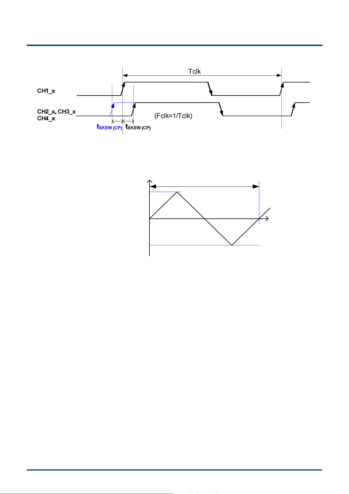
6. Input Channel Pair Skew Margin.
Note: x = 0, 1, 2, 3, 4
7. LVDS Receiver Clock SSCG (Spread spectrum clock generator) is defined as below figures.
1111////FFFF
SS
SS
SSSS
Fclk
Fclk____ss
FclkFclk
ss((((max
max))))
ssss
maxmax
Fclk
Fclk
FclkFclk
Fclk
Fclk____ss
FclkFclk
ss((((min
min))))
ssss
minmin
 Loading...