

AUO T550QVD01.0 Specification
:
0
T550QVD01.0 Product Specification
Rev.2 0
刪除
刪除
刪除刪除
Model Name: T550QVD01.0
刪除
刪除
: 1
Issue Date : 2011/12/20
( ) Preliminary Specifications
刪除刪除
刪除
刪除
刪除刪除
刪除
刪除
刪除刪除
: 09
: 0
(****) Final Specifications
Customer Signature Date AUO Date
Approved By
_________________________________
Note
Approval By PM Director
____________________________________
Reviewed By RD Director
____________________________________
Reviewed By Project Leader
____________________________________
刪除
刪除
: 1
刪除刪除
刪除
刪除: ****
刪除刪除
刪除
刪除
:
刪除刪除
格格格格式化
式化::::
縮排: 第一行: 7.5 字
式化式化
元
Prepared By PM
____________________________________
© Copyright AUO Optronics Corp. 2009 All Rights Reserved. Page 1 / 34
刪除
刪除
:
刪除刪除
Customer Signature
... [1]
:
0
T550QVD01.0 Product Specification
Rev.2 0
刪除
刪除
刪除刪除
Contents
No
CONTENTS
RECORD OF REVISIONS
1 GENERAL DESCRIPTION
2 ABSOLUTE MAXIMUM RATINGS
3 ELECTRICAL SPECIFICATION
3-1 ELECTRIACL CHARACTERISTICS
3-2 INTERFACE CONNECTIONS
3-3 SIGNAL TIMING SPECIFICATION
3-4 SIGNAL TIMING WAVEFORM
3-5 COLOR INPUT DATA REFERENCE
3-6 POWER SEQUENCE
3-7 BACKLIGHT SPECIFICATION
4 OPTICAL SPECIFICATION
5 MECHANICAL CHARACTERISTICS
6 RELIABILITY TEST ITEMS
7 INTERNATIONAL STANDARD
7-1 SAFETY
7-2 EMC
8 PACKING
8-1 DEFINITION OF LABEL
8-2 PACKING METHODS
8-3 PALLET AND SHIPMENT INFORMATION
9 PRECAUTION
9-1 MOUNTING PRECAUTIONS
/9-2 OPERATING PRECAUTIONS
9-3 ELECTROSTATIC DISCHARGE CONTROL
9-4 PRECAUTIONS FOR STRONG LIGHT EXPOSURE
9-5 STORAGE
9-6 HANDLING PRECAUTIONS FOR PROTECT FILM
© Copyright AUO Optronics Corp. 2009 All Rights Reserved. Page 2 / 34

:
0
Record of Revision
T550QVD01.0 Product Specification
Rev.2 0
刪除
刪除
刪除刪除
Version
Date Page Description
0.0 2011/08/12 First release
1.0 2011/09/27 Modify product specification
2.0 2011/11/11 Modify V by one interface
刪除
刪除
: 0.0
刪除刪除
刪除
刪除
: 2011/08/12
刪除刪除
刪除
刪除
: First release
刪除刪除
© Copyright AUO Optronics Corp. 2009 All Rights Reserved. Page 3 / 34
:
0
T550QVD01.0 Product Specification
Rev.2 0
1. General Description
This specification applies to the 55 inch Color TFT-LCD Module T550QVD01.0. This LCD module has a TFT active
matrix type liquid crystal 3,840*2,160 panel pixels, and diagonal size of 55 inch. This module supports 3,840*2,160 mode.
Each pixel is divided into Red, Green and Blue sub-pixels or dots which are arranged in vertical stripes. Gray scale or the
brightness of the sub-pixel color is determined with a 10-bit gray scale signal for each dot.
The T550QVD01.0 has been designed to apply the 10-bit , 16ch V by one interface method. It is intended to support
displays where high brightness, wide viewing angle, high color saturation, and high color depth are very important. Also,
3D function is also embedded into front glass
* General Information
Items Specification Unit Note
Active Screen Size 55 inch
Display Area 1209.6(H) x 680.4(V) mm
Outline Dimension 1242.6(H) x 715.4(V) x 16.2(Dmin) mm
Driver Element a-Si TFT active matrix
Bezel Opening 1218.6(H) x 689.4(V) mm
Display Colors 10 bit, Colors
Number of Pixels 3840 x 3 x 2160 Pixel
Pixel Pitch 0.315(H) x 0.315(W) mm
Pixel Arrangement RGB vertical stripe
Display Operation Mode Normally Black
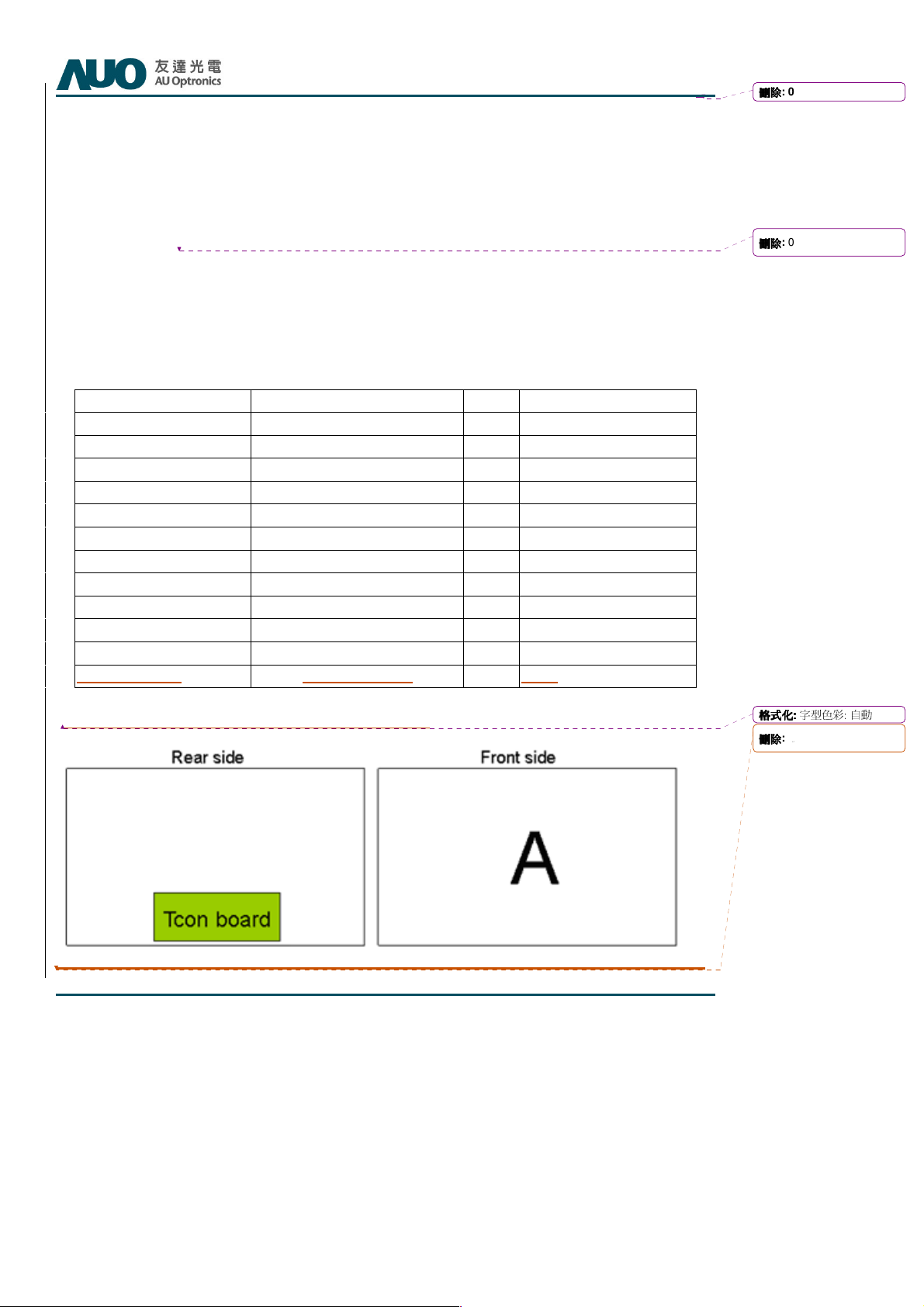
Rotate Function Unachievable Note 1
Display Orientation Signal input with “A” Note 2
Note 1: Rotate Function refers to LCD display could be able to rotate.
Note 2: LCD display as below illustrated when signal input with “A”.
刪除
刪除
刪除刪除
刪除
刪除
刪除刪除
格格格格式化
式化::::
式化式化
刪除
刪除
刪除刪除
: 0
:
字型色彩: 自動
© Copyright AUO Optronics Corp. 2009 All Rights Reserved. Page 4 / 34

:
0
T550QVD01.0 Product Specification
2. Absolute Maximum Ratings
The followings are maximum values which, if exceeded, may cause faulty operation or damage to the unit
Item Symbol Min Max Unit Conditions
Logic/LCD Drive Voltage (for
12V input)
Logic/LCD Drive Voltage (for 5V
input)
Input Voltage of Signal (for 12V
input)
Input Voltage of Signal (for 5V
input)
Operating Temperature TOP 0 +50 [oC] Note 2
Operating Humidity HOP 10 90 [%RH] Note 2
Storage Temperature TST -20 +60 [oC] Note 2
Storage Humidity HST 10 90 [%RH] Note 2
Panel Surface Temperature PST - 65 [oC] Note 3
Vcc -0.3 14 [Volt] Note 1
Vcc [Volt] Note 1
Vin -0.3 3.6 [Volt] Note 1
Vin [Volt] Note 1
Rev.2 0
刪除
刪除
刪除刪除
Note 1: Duration:50 msec.
Note 2 : Maximum Wet-Bulb should be 39 and No condensation.℃
The relative humidity must not exceed 90% non-condensing at temperatures of 40 or less. At temperatures greater
than 40 , the wet bulb temperature must not exceed 39 .
℃ ℃
Note 3: Surface temperature is measured at 50℃ Dry condition
℃
© Copyright AUO Optronics Corp. 2009 All Rights Reserved. Page 5 / 34
:
0
T550QVD01.0 Product Specification
Rev.2 0
3. Electrical Specification
The T550QVD01 .0 requires two power inputs. One is employed to power the LCD electronics and to drive the TFT array
and liquid crystal. The other is to power Back Light Unit.
3.1 Electrical Characteristics
3.1.1: DC Characteristics
刪除
刪除
刪除刪除
刪除
刪除
刪除刪除
: ( TBD )
Parameter Symbol
Min. Typ. Max
Value
Unit Note
LCD
Power Supply Input Voltage (for input power=12V) VDD 10.8 12 13.2 VDC
Power Supply Input Current (Define to section:1.1) IDD -- 1.9 4.5 A 1
Power Consumption (Define to section:1.1) PC -- 22.8 54 Watt 1
Inrush Current (Define to section:1.1) I
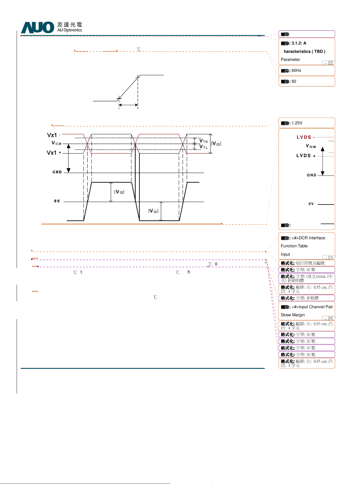
Input Differential Voltage
V by One
Interface
Differential Input High Threshold Voltage VTH +50 mVDC 3
Differential Input Low Threshold Voltage VTL -50 mVDC 3
Input Common Mode Voltage V
CMOS
Interface
Input High Threshold Voltage
Input Low Threshold Voltage
-- -- 4 A 2
RUSH
∣
V
∣
100 mVDC 3
ID
0.82 VDC 3
ICM
VIH
(High)
VIL
(Low)
2.4 -- 3.3 VDC 4
0 -- 0.6 VDC 4
Backlight Power Consumption PBL 137 Watt
Life time (MTTF) 30000
Hour 5,6
刪除
刪除
刪除刪除
刪除
刪除
刪除刪除
格格格格式化
式化::::
式化式化
格格格格式化
式化::::
式化式化
刪除
刪除
刪除刪除
格格格格式化
式化::::
式化式化
刪除
刪除
刪除刪除
格格格格式化
式化::::
式化式化
刪除
刪除
刪除刪除
格格格格式化
式化::::
式化式化
刪除
刪除
刪除刪除
刪除
刪除
刪除刪除
刪除
刪除
刪除刪除
刪除
刪除
刪除刪除
刪除
刪除
刪除刪除
: TBD
: TBD
: TBD
: TBD
: --
: TBD
: 5
: 5
: 150
: 9
字型色彩: 自動
字型色彩: 自動
字型色彩: 自動
字型色彩: 自動
字型色彩: 自動
© Copyright AUO Optronics Corp. 2009 All Rights Reserved. Page 6 / 34
刪除
刪除
刪除刪除
: 10
s
µ
:
0
Input Channel Pair
Note :
1. V
= 12.0V, Fv = 120Hz, Fclk= 78.125MHz , 25 , Test Pattern : White Pattern℃
DD
>> refer to “Section:3.3 Signal Timing Specification, Typical timing”
2. Measurement condition : Rising time = 400us
90%
T550QVD01.0 Product Specification
VVVV
DD
DD
DDDD
Rev.2 0
刪除
刪除
刪除刪除
刪除
刪除
: 3.1.2: AC
刪除刪除
Characteristics ( TBD )
Parameter
刪除
刪除
: 60Hz
刪除刪除
刪除
刪除
: 82
刪除刪除
... [2]
GND
GND
GNDGND
10%
400
400
400400
3. V
= 0.82V
ICM
4. The measure points of V
5. The relative humidity must not exceed 80% non-condensing at temperatures of 40℃ or less. At temperatures
greater than 40℃, the wet bulb temperature must not exceed 39℃. W hen operate at low temperatures, the
brightness of LED will drop and the life time of LED will be reduced.
6. The lifetime (MTTF) is defined as the time which luminance of LED is 50% compared to its original value.
[Operating condition: Continuous operating at Ta = 25±2℃]
© Copyright AUO Optronics Corp. 2009 All Rights Reserved. Page 7 / 34
IH
and V
are in LCM side after connecting the System Board and LCM.
IL
刪除
刪除
: 1.25V
刪除刪除
L V DS -
V
L V DS +
刪除
刪除
:
刪除刪除
刪除
刪除
: <#>DCR Interface:
刪除刪除
Function Table
Input
格格格格式化
式化::::
項目符號及編號
式化式化
格格格格式化
式化::::
字型: 10 點
式化式化
格格格格式化
式化::::
字型: (英文)Arial, (中
式化式化
文) 新細明體
格格格格式化
式化::::
縮排: 左: 0.85 cm, 凸
式化式化
出: 4 字元
格格格格式化
式化::::
字型: 非粗體
式化式化
刪除
刪除
: <#>
刪除刪除
Skew Margin
格格格格式化
式化::::
縮排: 左: 0.85 cm, 凸
式化式化
出: 4 字元
格格格格式化
式化::::
字型: 10 點
式化式化
格格格格式化
式化::::
字型: 10 點
式化式化
格格格格式化
式化::::
字型: 10 點
式化式化
格格格格式化
式化::::
字型: 10 點
式化式化
格格格格式化
式化::::
縮排: 左: 0.85 cm, 凸
式化式化
出: 4 字元
IC M
G N D
0 V
... [3]
... [4]

:
0
T550QVD01.0 Product Specification
3.2 Interface Connections
LCD V by One connector:
V by One CN (41Pin) : FI-RE41S-HF (JAE)
PIN Symbol Description PIN Symbol Description
GND Ground
1
GND Ground
2
GND Ground
3
GND Ground
4
GND Ground
5
SCL I2C CLK
6
SDA I2C Data
7
GND CML Ground
8
Rx8n V-by-One HS Data Lane 8
9
Rx8p V-by-One HS Data Lane 8
10
GND CML Ground
11
GND CML Ground
12
Rx9n V-by-One HS Data Lane 9
13
Rx9p V-by-One HS Data Lane 9
14
GND CML Ground
15
GND CML Ground
16
Rx10n V-by-One HS Data Lane 10
17
Rx10p V-by-One HS Data Lane 10
18
GND CML Ground
19
GND CML Ground
20
21
22
23
24
25
26
27
28
29
30
31
32
33
34
35
36
37
38
39
40
41
V by One CN (51Pin) : FI-RE51S-HF (JAE)
PIN Symbol Description PIN
1
2
3
4
5
6
7
8
9
10
11
12
13
14
15
16
17
NC
NC
NC
NC
NC
NC
NC
NC
NC AUO Internal Use Only
NC
GND
GND Ground
GND Ground
GND Ground
GND Ground
HTPDN Hot plug detect
LOCKN Lock detect
NC PIN
26
NC PIN
27
AUO Internal Use Only
NC PIN
29
NC PIN
30
NC PIN
31
NC PIN
32
NC PIN
33
NC PIN
35
Ground 36
28
© Copyright AUO Optronics Corp. 2009 All Rights Reserved. Page 8 / 34
Rx11n V-by-One HS Data Lane 11
Rx11p V-by-One HS Data Lane 11
GND CML Ground
GND CML Ground
Rx12n V-by-One HS Data Lane 12
Rx12p V-by-One HS Data Lane 12
GND CML Ground
GND CML Ground
Rx13n V-by-One HS Data Lane 13
Rx13p V-by-One HS Data Lane 13
GND CML Ground
GND CML Ground
Rx14n V-by-One HS Data Lane 14
Rx14p V-by-One HS Data Lane 14
GND CML Ground
GND CML Ground
Rx15n V-by-One HS Data Lane 15
Rx15p V-by-One HS Data Lane 15
GND CML Ground
NC AUO Internal Use Only
GND Ground
Symbol Description
GND CML Ground
Rx2n V-by-One HS Data Lane 2
Rx2p V-by-One HS Data Lane 2
GND CML Ground
GND CML Ground
Rx3n V-by-One HS Data Lane 3
Rx3p V-by-One HS Data Lane 3
GND CML Ground
34
37
38
39
40
41
42
GND CML Ground
Rx4n V-by-One HS Data Lane 4
Rx4p V-by-One HS Data Lane 4
GND CML Ground
GND CML Ground
Rx5n V-by-One HS Data Lane 5
Rx5p V-by-One HS Data Lane 5
GND CML Ground
GND CML Ground
Rev.2 0
刪除
刪除
刪除刪除
刪除
刪除
: FI-RE51S-HF (JAE)
刪除刪除
刪除
刪除
: PIN
刪除刪除
刪除
刪除
: 1
刪除刪除
刪除
刪除
: 21
刪除刪除
刪除
刪除
: GND
刪除刪除
刪除
刪除
: Rx11n
刪除刪除
刪除
刪除
: 2
刪除刪除
刪除
刪除
: Rx11p
刪除刪除
刪除
刪除
: 3
刪除刪除
刪除
刪除
: GND
刪除刪除
刪除
刪除
: 4
刪除刪除
刪除
刪除
: GND
刪除刪除
刪除
刪除
: 5
刪除刪除
刪除
刪除
: Rx12n
刪除刪除
刪除
刪除
: 6
刪除刪除
刪除
刪除
: Rx12p
刪除刪除
刪除
刪除
: 7
刪除刪除
刪除
刪除
: 27
刪除刪除
刪除
刪除
: SDA
刪除刪除
刪除
刪除
: GND
刪除刪除
刪除
刪除
: 8
刪除刪除
刪除
刪除
: 28
刪除刪除
刪除
刪除
: GND
刪除刪除
刪除
刪除
: GND
刪除刪除
刪除
刪除
: 9
刪除刪除
刪除
刪除
: 29
刪除刪除
刪除
刪除
: Rx8n
刪除刪除
刪除
刪除
: Rx13n
刪除刪除
刪除
刪除
: 10
刪除刪除
刪除
刪除
: 30
刪除刪除
刪除
刪除
: Rx8p
刪除刪除
刪除
刪除
: Rx13p
刪除刪除
刪除
刪除
: 11
刪除刪除
刪除
刪除
: 31
刪除刪除
刪除
刪除
: GND
刪除刪除
... [5]
... [6]
... [7]
... [8]
... [9]
... [10]
... [11]
... [12]
... [13]
... [14]
... [15]
... [16]
... [17]
... [18]
... [19]
... [20]
... [21]
... [22]
... [23]
... [24]
... [25]
... [26]
... [27]
... [28]
... [29]
... [30]
... [31]
:
0
T550QVD01.0 Product Specification
18
19
20
21
22
23
24
25
GND CML Ground
Rx0n V-by-One HS Data Lane 0
Rx0p V-by-One HS Data Lane 0
GND CML Ground
GND CML Ground
Rx1n V-by-One HS Data Lane 1
Rx1p V-by-One HS Data Lane 1
GND CML Ground
51
43
44
45
46
47
48
49
50
Rx6n V-by-One HS Data Lane 6
Rx6p V-by-One HS Data Lane 6
GND CML Ground
GND CML Ground
Rx7n V-by-One HS Data Lane 7
Rx7p V-by-One HS Data Lane 7
GND CML Ground
NC AUO Internal Use Only
SYNC3D_I 3D Sync. In Flag
LCD Power connector:
Power CN (12Pin) : A2010WR0-12PS-SHP (JWT)
PIN Symbol Description
1
2
3
4
5
6
7
8
9
10
11
12
PWR Power V12 IN
PWR Power V12 IN
PWR Power V12 IN
PWR Power V12 IN
PWR Power V12 IN
NC
NC
GND Ground
GND Ground
GND Ground
GND Ground
GND Ground
PWR Power V12 IN
PWR Power V12 IN
PWR Power V12 IN
PWR Power V12 IN
PWR Power V12 IN
NC PIN
NC PIN
GND Ground
GND Ground
GND Ground
GND Ground
GND Ground
刪除
刪除
刪除刪除
刪除
刪除
: 18
刪除刪除
刪除
刪除
: 43
刪除刪除
Rev.2 0
(Glasses type)
刪除
刪除
刪除刪除
刪除
刪除
刪除刪除
刪除
刪除
刪除刪除
刪除
刪除
刪除刪除
刪除
刪除
刪除刪除
刪除
刪除
刪除刪除
刪除
刪除
刪除刪除
刪除
刪除
刪除刪除
刪除
刪除
刪除刪除
刪除
刪除
刪除刪除
刪除
刪除
刪除刪除
刪除
刪除
刪除刪除
刪除
刪除
刪除刪除
刪除
刪除
刪除刪除
刪除
刪除
刪除刪除
刪除
刪除
刪除刪除
刪除
刪除
刪除刪除
: GND
: Rx6n
: 19
: 44
: Rx0n
: Rx6p
: 20
: 45
: Rx0p
: GND
: 21
: 46
: GND
: 22
: Rx7n
: 23
: 48
... [41]
... [42]
... [43]
... [44]
... [45]
... [46]
... [47]
... [48]
... [49]
... [50]
刪除
刪除
: Rx1n
刪除刪除
刪除
刪除
刪除刪除
刪除
刪除
刪除刪除
: Rx7p
: 24
... [51]
... [52]
© Copyright AUO Optronics Corp. 2009 All Rights Reserved. Page 9 / 34
刪除
刪除
: 49
刪除刪除
刪除
刪除
: Rx1p
刪除刪除
刪除
刪除
: GND
刪除刪除
刪除
刪除
: 25
刪除刪除
刪除
刪除
: 50
刪除刪除
刪除
刪除
: GND
刪除刪除
刪除
刪除
: NC
刪除刪除
刪除
刪除
: AGIN
刪除刪除
刪除
刪除
: AUO Internal Use
刪除刪除
格格格格式化
式化::::
字型色彩: 自動
式化式化
刪除
刪除
: Aging Mode
刪除刪除
格格格格式化
式化::::
字型色彩: 自動
式化式化
刪除
刪除
: 51
刪除刪除
刪除
刪除
: SYNC3D_I
刪除刪除
... [53]
... [54]
... [55]
... [56]
... [57]
... [58]
... [59]
... [60]
... [61]
... [62]

:
0
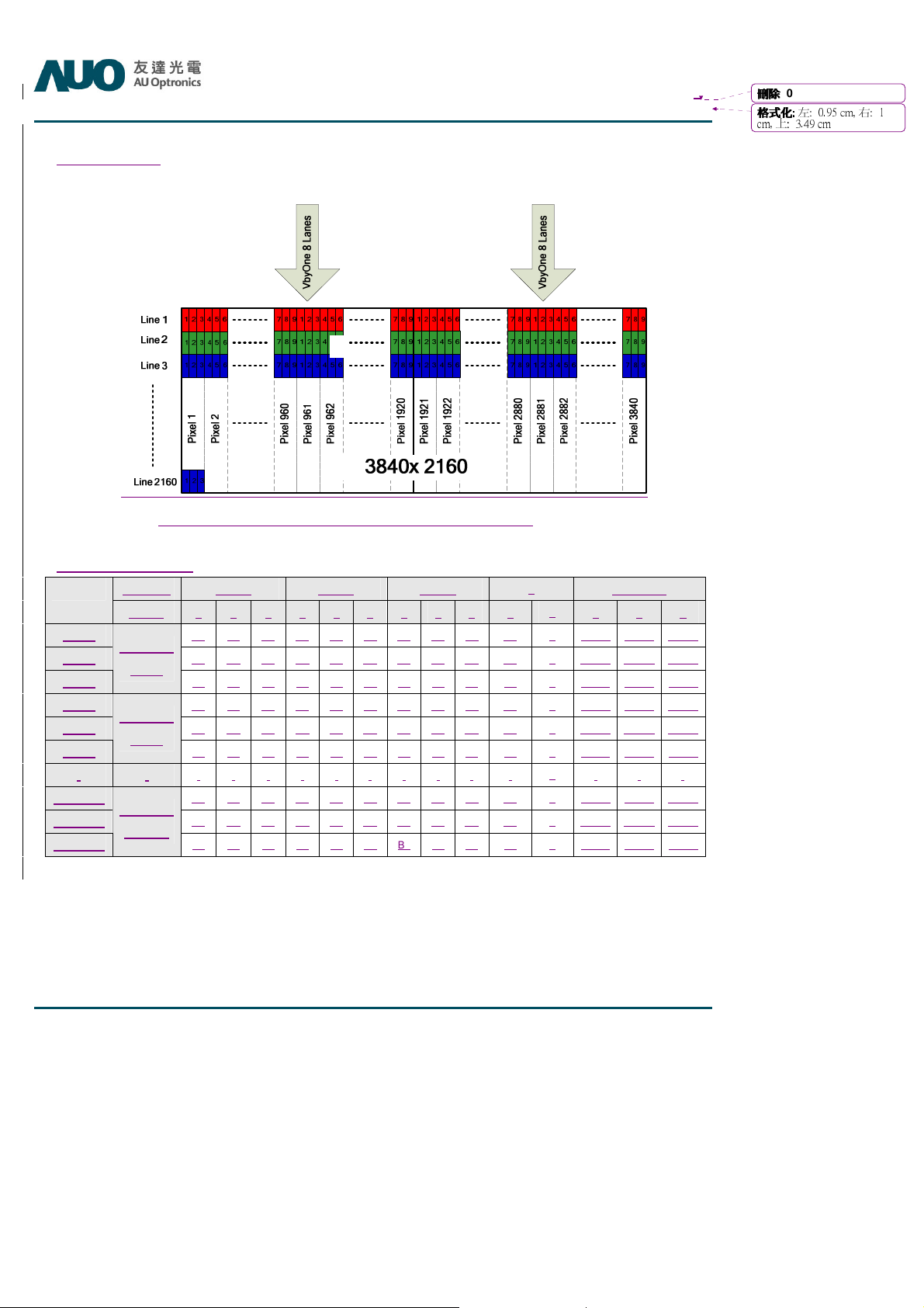
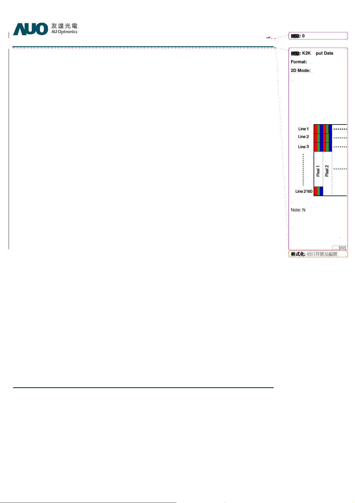
4 K2K Input Data Format:
2D Mode:
2D Mode Pixel Mapping:
Pixel No Pixel 1 Pixel 2 Pixel 3
Line 1
Line 2
Line 3
Line 4
Line 5
Line 6
:
Line 2158
Line 2159
Line 2160
T550QVD01.0 Product Specification
Note: Normal pixel data mapping
~
R1 G1 B1 R2 G2 B2 R3 G3 B3 R4 ~ R3840 G3840 B3840
R1 G1 B1 R2 G2 B2 R3 G3 B3 R4 ~ R3840 G3840 B3840
R1 G1 B1 R2 G2 B2 R3 G3 B3 R4 ~ R3840 G3840 B3840
R1 G1 B1 R2 G2 B2 R3 G3 B3 R4 ~ R3840 G3840 B3840
R1 G1 B1 R2 G2 B2 R3 G3 B3 R4 ~ R3840 G3840 B3840
R1 G1 B1 R2 G2 B2 R3 G3 B3 R4 ~ R3840 G3840 B3840
: : : : : : : : : :
R1 G1 B1 R2 G2 B2 R3 G3 B3 R4 ~ R3840 G3840 B3840
R1 G1 B1 R2 G2 B2 R3 G3 B3 R4 ~ R3840 G3840 B3840
R1 G1 B1 R2 G2 B2 R3 G3 B3 R4 ~ R3840 G3840 B3840
~
Pixel 3840
: : :
Rev.2 0
刪除
刪除
刪除刪除
© Copyright AUO Optronics Corp. 2009 All Rights Reserved. Page 10 / 34
:
0
3D Mode (9-View)
T550QVD01.0 Product Specification
Rev.2 0
G7
刪除
刪除
刪除刪除
格格格格式化
式化::::
左: 0.95 cm, 右: 1
式化式化
cm, 上: 3.49 cm
Note: 3D multi-view data mapping (1,2,3,4,5,6,7,8,9 is the viewing number)
3D Mode Pixel Mapping:
Pixel No.
View # 1 2 3 4 5 6 7 8 9 1
Line 1
Line 2
Line 3
Line 4
Line 5
Line 6
Multi-view
Line 1
Multi-view
Line 2
: :
Line 2158
Line 2159
Line 2160
Multi-view
Line 720
~
Pixel 1 Pixel 2 Pixel 3
R1 R1 R1 R1 R1 R1 R1 R1 R1 R2 ~ R1280 R1280 R1280
G1 G1 G1 G1 G1 G1 G1 G1 G1 G2 ~ G1280 G1280 G1280
B1 B1 B1 B1 B1 B1 B1 B1 B1 B2 ~ B1280 B1280 B1280
R1 R1 R1 R1 R1 R1 R1 R1 R1 R2 ~ R1280 R1280 R1280
G1 G1 G1 G1 G1 G1 G1 G1 G1 G2 ~ G1280 G1280 G1280
B1 B1 B1 B1 B1 B1 B1 B1 B1 B2 ~ B1280 B1280 B1280
: : : : : : : : : : ~ : : :
R1 R1 R1 R1 R1 R1 R1 R1 R1 R2 ~ R1280 R1280 R1280
G1 G1 G1 G1 G1 G1 G1 G1 G1 G2 ~ G1280 G1280 G1280
B1 B1 B1 B1 B1 B1 B1 B1 B1 B2 ~ B1280 B1280 B1280
~
Pixel 3840
7 8 9
© Copyright AUO Optronics Corp. 2009 All Rights Reserved. Page 11 / 34
:
0
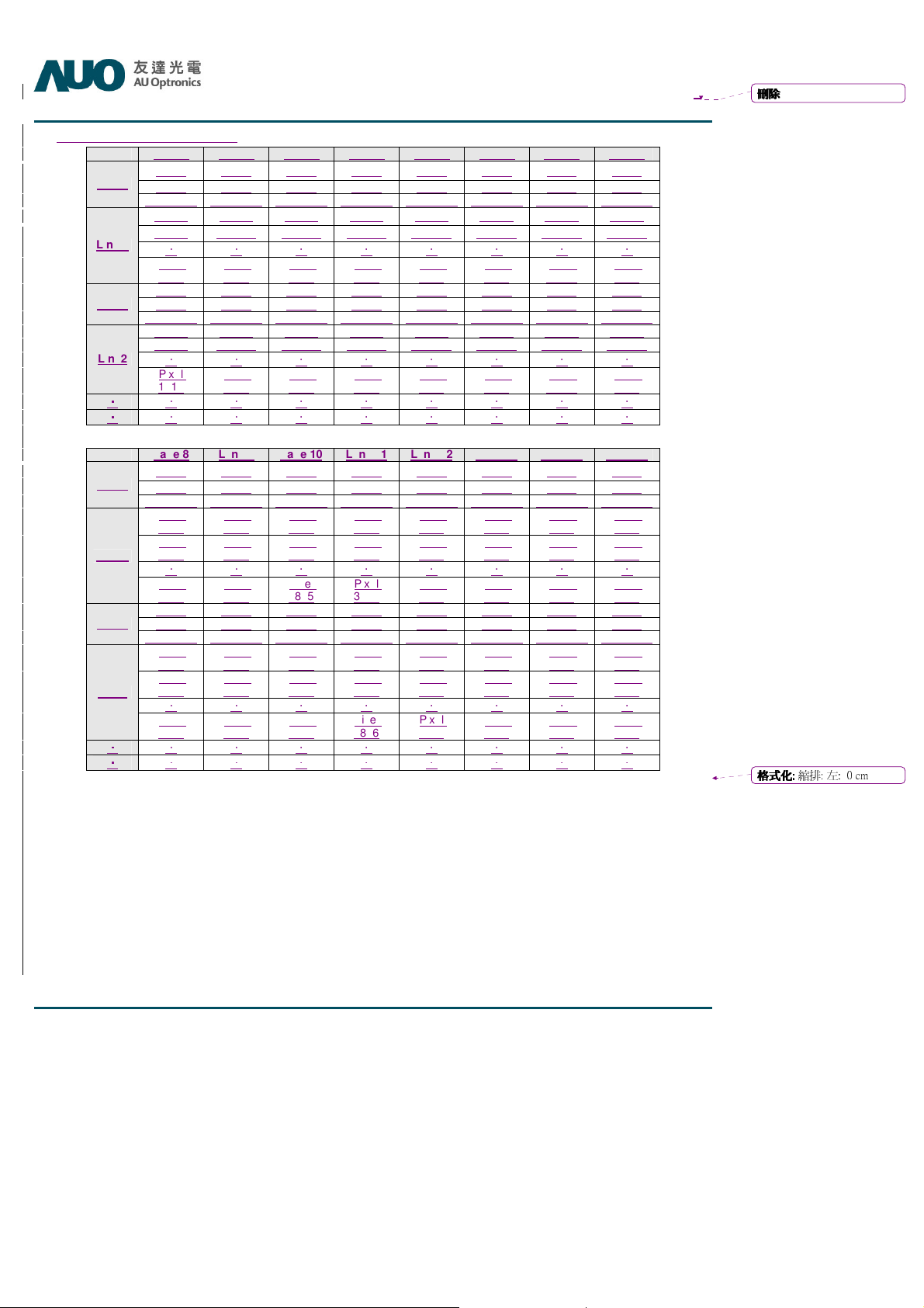
V-by-One Lanes of Pixel Data :
Lane 0 Lane 1 Lane 2 Lane 3 Lane 4 Lane 5 Lane 6 Lane 7
Blank
Line 1
Blank
Line2
....
....
Blank
Line 1
Blank
Line2
....
....
FSBS FSBS FSBS FSBS FSBS FSBS FSBS FSBS
FSBP FSBP FSBP FSBP FSBP FSBP FSBP FSBP
FSBE_SR FSBE_SR FSBE_SR FSBE_SR FSBE_SR FSBE_SR FSBE_SR FSBE_SR
Pixel 1 Pixel 2 Pixel 3 Pixel 4 Pixel 5 Pixel 6 Pixel 7 Pixel 8
Pixel 9 Pixel 10 Pixel 11 Pixel 12 Pixel 13 Pixel 14 Pixel 15 Pixel 16
.
Pixel
1913
FSBS FSBS FSBS FSBS FSBS FSBS FSBS FSBS
FSBP FSBP FSBP FSBP FSBP FSBP FSBP FSBP
FSBE_SR FSBE_SR FSBE_SR FSBE_SR FSBE_SR FSBE_SR FSBE_SR FSBE_SR
Pixel 1 Pixel 2 Pixel 3 Pixel 4 Pixel 5 Pixel 6 Pixel 7 Pixel 8
Pixel 8 Pixel 10 Pixel 11 Pixel 12 Pixel 13 Pixel 14 Pixel 15 Pixel 16
.
Pixel
1913
Lane 8 Lane 9 Lane 10 Lane 11 Lane 12 Lane 13 Lane 14 Lane 15
.
.
FSBS FSBS FSBS FSBS FSBS FSBS FSBS FSBS
FSBP FSBP FSBP FSBP FSBP FSBP FSBP FSBP
FSBE_SR FSBE_SR FSBE_SR FSBE_SR FSBE_SR FSBE_SR FSBE_SR FSBE_SR
Pixel
1921
Pixel
1929
.
Pixel
3833
FSBS FSBS FSBS FSBS FSBS FSBS FSBS FSBS
FSBP FSBP FSBP FSBP FSBP FSBP FSBP FSBP
FSBE_SR FSBE_SR FSBE_SR FSBE_SR FSBE_SR FSBE_SR FSBE_SR FSBE_SR
Pixel
1921
Pixel
1929
.
Pixel
3833
.
.
.
Pixel
1914
.
Pixel
1914
.
.
Pixel
1922
Pixel
1930
.
Pixel
3834
Pixel
1922
Pixel
1930
.
Pixel
3834
.
.
T550QVD01.0 Product Specification
Rev.2 0
.
Pixel
1915
.
Pixel
1915
.
.
Pixel
1923
Pixel
1931
.
Pixel
3835
Pixel
1923
Pixel
1931
.
Pixel
3835
.
.
.
Pixel
1916
.
Pixel
1916
.
.
Pixel
1924
Pixel
1932
.
Pixel
3836
Pixel
1924
Pixel
1932
.
Pixel
3836
.
.
.
Pixel
1917
.
Pixel
1917
.
.
Pixel
1925
Pixel
1933
.
Pixel
3837
Pixel
1925
Pixel
1933
.
Pixel
3837
.
.
.
Pixel
1918
.
Pixel
1918
.
.
Pixel
1926
Pixel
1934
.
Pixel
3838
Pixel
1926
Pixel
1934
.
Pixel
3838
.
.
.
Pixel
19198
.
Pixel
19198
.
.
Pixel
1927
Pixel
1935
.
Pixel
3839
Pixel
1927
Pixel
1935
.
Pixel
3839
.
.
.
Pixel
1920
.
Pixel
1920
.
.
Pixel
1928
Pixel
1936
.
Pixel
3840
Pixel
1928
Pixel
1936
.
Pixel
3840
.
.
刪除
刪除
刪除刪除
格格格格式化
式化::::
式化式化
縮排: 左: 0 cm
© Copyright AUO Optronics Corp. 2009 All Rights Reserved. Page 12 / 34
:
0
T550QVD01.0 Product Specification
Rev.2 0
刪除
刪除
刪除刪除
刪除
刪除
: K2K Input Data
刪除刪除
Format:
2D Mode:
Note: Normal pixel data
mapping
2D Mode Pixel Mapping:
Pixel No
格格格格式化
式化::::
項目符號及編號
式化式化
... [69]
© Copyright AUO Optronics Corp. 2009 All Rights Reserved. Page 13 / 34

:
0
T550QVD01.0 Product Specification
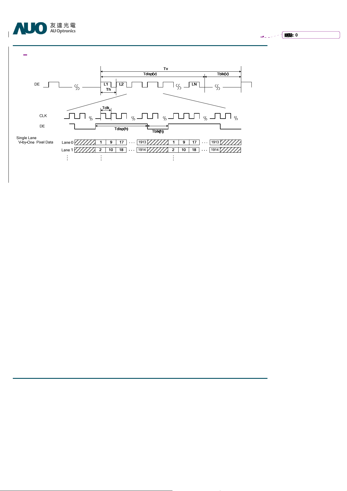
3.3 Signal Timing Specification
This is the signal timing required at the input of the user connector. All of the interface signal timing should be satisfied
with the following specifications for its proper operation.
4K2K (3840x2160) V-by-One Each Lane Timing Spec. (240x2160 @120Hz x16Lanes)
Type Item Symbol Min Typ Max Unit
Vertical Section
Active Tdisp(v) 2160 Th
Blanking Tblk(v) 12 40 84 Th
Period Th 280 290 300 Tclk
Period Tv 2172 2200
Horizontal Section
Active Tdisp(h) 240 Tclk
Blanking Tblk(h) 40 50 60 Tclk
Frequency Clock Tclk 76.48 78.125 MHz
4K2K (3840x2160) V-by-One Each Lane Timing Spec. (240x2160 @100Hz x16Lanes)
Type Item Symbol Min Typ Max Unit
Period Tv 2172 2200
Vertical Section
Active Tdisp(v) 2160 Th
Blanking Tblk(v) 12 40 532 Th
Period Th 280 290 354 Tclk
Horizontal Section
Active Tdisp(h) 240 Tclk
Blanking Tblk(h) 40 50 114 Tclk
Frequency Clock Tclk 76.48 78.125 MHz
4K2K V-by-One 2area (1920x2160) Timing difference
Type Item Symbol Min Typ Max Unit
2Area Latency Difference
Tdiff -1 0
2244
2692
1
Th
Th
Th
Rev.2 0
刪除
刪除
刪除刪除
© Copyright AUO Optronics Corp. 2009 All Rights Reserved. Page 14 / 34
:
0
3.4
Signal Timing Waveforms
T550QVD01.0 Product Specification
Rev.2 0
刪除
刪除
刪除刪除
© Copyright AUO Optronics Corp. 2009 All Rights Reserved. Page 15 / 34
:
0
T550QVD01.0 Product Specification
Rev.2 0
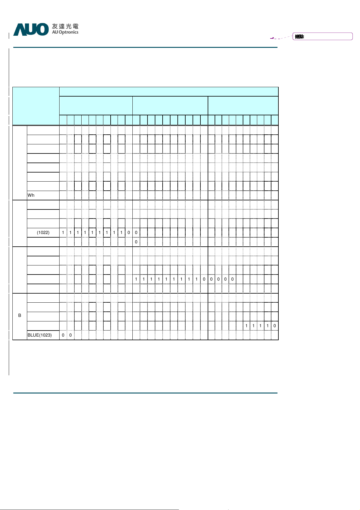
3.5 Color Input Data Reference
The brightness of each primary color (red, green and blue) is based on the 10 bit gray scale data input for the color; the
higher the binary input, the brighter the color. The table below provides a reference for color versus data input.
COLOR DATA REFERENCE
Input Color Data
Color
Black 0 0 0 0 0 0 0 0 0 0 0 0 0 0 0 0 0 0 0 0 0 0 0 0 0 0 0 0 0 0
Red(1023) 1 1 1 1 1 1 1 1 1 1 0 0 0 0 0 0 0 0 0 0 0 0 0 0 0 0 0 0 0 0
Green(1023) 0 0 0 0 0 0 0 0 0 0 1 1 1 1 1 1 1 1 1 1 0 0 0 0 0 0 0 0 0 0
Basic
Blue(1023) 0 0 0 0 0 0 0 0 0 0 0 0 0 0 0 0 0 0 0 0 1 1 1 1 1 1 1 1 1 1
Color
Cyan 0 0 0 0 0 0 0 0 0 0 1 1 1 1 1 1 1 1 1 1 1 1 1 1 1 1 1 1 1 1
Magenta 1 1 1 1 1 1 1 1 1 1 0 0 0 0 0 0 0 0 0 0 1 1 1 1 1 1 1 1 1 1
Yellow 1 1 1 1 1 1 1 1 1 1 1 1 1 1 1 1 1 1 1 1 0 0 0 0 0 0 0 0 0 0
White 1 1 1 1 1 1 1 1 1 1 1 1 1 1 1 1 1 1 1 1 1 1 1 1 1 1 1 1 1 1
RED(000) 0 0 0 0 0 0 0 0 0 0 0 0 0 0 0 0 0 0 0 0 0 0 0 0 0 0 0 0 0 0
RED(001) 0 0 0 0 0 0 0 0 0 1 0 0 0 0 0 0 0 0 0 0 0 0 0 0 0 0 0 0 0 0
R
----
RED(1022) 1 1 1 1 1 1 1 1 1 0 0 0 0 0 0 0 0 0 0 0 0 0 0 0 0 0 0 0 0 0
RED(1023) 1 1 1 1 1 1 1 1 1 1 0 0 0 0 0 0 0 0 0 0 0 0 0 0 0 0 0 0 0 0
GREEN(000) 0 0 0 0 0 0 0 0 0 0 0 0 0 0 0 0 0 0 0 0 0 0 0 0 0 0 0 0 0 0
GREEN(001) 0 0 0 0 0 0 0 0 0 0 0 0 0 0 0 0 0 0 0 1 0 0 0 0 0 0 0 0 0 0
G
----
GREEN(1022) 0 0 0 0 0 0 0 0 0 0 1 1 1 1 1 1 1 1 1 0 0 0 0 0 0 0 0 0 0 0
GREEN(1023) 0 0 0 0 0 0 0 0 0 0 1 1 1 1 1 1 1 1 1 1 0 0 0 0 0 0 0 0 0 0
BLUE(000) 0 0 0 0 0 0 0 0 0 0 0 0 0 0 0 0 0 0 0 0 0 0 0 0 0 0 0 0 0 0
BLUE(001) 0 0 0 0 0 0 0 0 0 0 0 0 0 0 0 0 0 0 0 0 0 0 0 0 0 0 0 0 0 1
B
----
BLUE(1022) 0 0 0 0 0 0 0 0 0 0 0 0 0 0 0 0 0 0 0 0 1 1 1 1 1 1 1 1 1 0
BLUE(1023) 0 0 0 0 0 0 0 0 0 0 0 0 0 0 0 0 0 0 0 0 1 1 1 1 1 1 1 1 1 1
MSB LSB
R9 R8 R7 R6 R5 R4 R3 R2 R1 R0 G9 G8 G7 G6 G5 G4 G3 G2 G1 G0 B9 B8 B7 B6 B5 B4 B3 B2 B1 B0
RED
MSB LSB
GREEN
MSB LSB
BLUE
刪除
刪除
刪除刪除
© Copyright AUO Optronics Corp. 2009 All Rights Reserved. Page 16 / 34
:
0
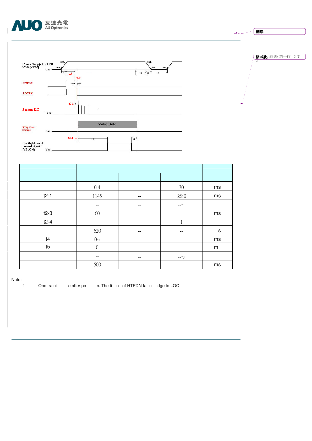
3.6 Power Sequence for LCD
T550QVD01.0 Product Specification
Rev.2 0
刪除
刪除
刪除刪除
格格格格式化
式化::::
縮排: 第一行: 2 字
式化式化
元
Parameter
Unit
Min. Type. Max.
Values
t1
t2-1
t2-2
t2-3
t2-4
t3
t4
t5
t6
t7
Note:
(1) t2-1 : V by One training time after power-on. The timing of HTPDN falling edge to LOCKN falling edge decided by
customer system.
(1) t4=0 : concern for residual pattern before BLU turn off.
(2) t6 : voltage of VDD must decay smoothly after power-off. (Customer system decide this value)
0.4 -- 30
1145 -- 3580
-- -- --*1
60 -- --
1
620 -- --
0*2 -- --
0
--
500
-- --
-- --*3
-- --
ms
ms
ms
ms
ms
ms
ms
ms
ms
ms
© Copyright AUO Optronics Corp. 2009 All Rights Reserved. Page 17 / 34
:
0
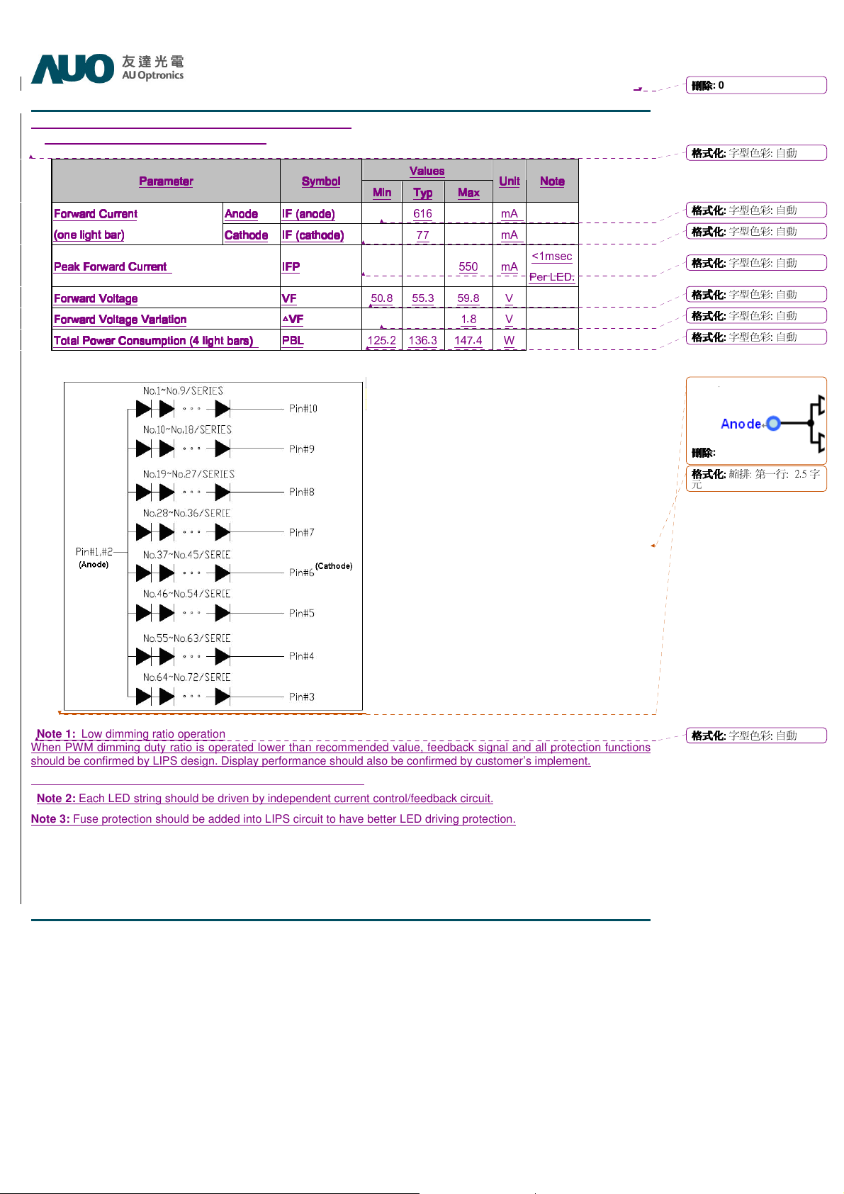
3.7 Backlight Specification (without driver board)
3.7.1 Light bar Driven Condition
PPPParameter
arameter Symbol
arameterarameter
Anode
Forward Current
Forward Current
Forward CurrentForward Current
(one light bar)
(one light bar)
(one light bar)(one light bar)
Peak Forward Current
Peak Forward Current IFP
Peak Forward Current Peak Forward Current
Forward Voltage
Forward Voltage VF
Forward VoltageForward Voltage
Forward Voltage Varia
Forward Voltage Variation
Forward Voltage VariaForward Voltage Varia
Total Power Consumption (4 light bars)
Total Power Consumption (4 light bars) PBL
Total Power Consumption (4 light bars) Total Power Consumption (4 light bars)
tion △△△△VF
tiontion
Anode IF (anode)
AnodeAnode
Cathode
Cathode IF (cathode)
CathodeCathode
Symbol
SymbolSymbol
IF (anode)
IF (anode)IF (anode)
IF (cathode)
IF (cathode)IF (cathode)
IFP
IFPIFP
VF
VFVF
VF
VFVF
PBL
PBLPBL
T550QVD01.0 Product Specification
Values
Values
ValuesValues
Min
Min Typ
Typ Max
MinMin
TypTyp
616 mA
77 mA
550 mA
50.8 55.3 59.8 V
1.8 V
125.2 136.3 147.4 W
Max
MaxMax
Unit
Unit
UnitUnit
<1msec
Per LED.
Note
Note
NoteNote
Rev.2 0
刪除
刪除
刪除刪除
格格格格式化
式化::::
字型色彩: 自動
式化式化
格格格格式化
式化::::
字型色彩: 自動
式化式化
格格格格式化
式化::::
字型色彩: 自動
式化式化
格格格格式化
式化::::
字型色彩: 自動
式化式化
格格格格式化
式化::::
字型色彩: 自動
式化式化
格格格格式化
式化::::
字型色彩: 自動
式化式化
格格格格式化
式化::::
字型色彩: 自動
式化式化
刪除
刪除
:
刪除刪除
格格格格式化
式化::::
縮排: 第一行: 2.5 字
式化式化
元
Note 1: Low dimming ratio operation
When PWM dimming duty ratio is operated lower than recommended value, feedback signal and all protection functions
should be confirmed by LIPS design. Display performance should also be confirmed by customer’s implement.
Note 2: Each LED string should be driven by independent current control/feedback circuit.
Note 3: Fuse protection should be added into LIPS circuit to have better LED driving protection.
© Copyright AUO Optronics Corp. 2009 All Rights Reserved. Page 18 / 34
格格格格式化
式化::::
式化式化
字型色彩: 自動
:
0
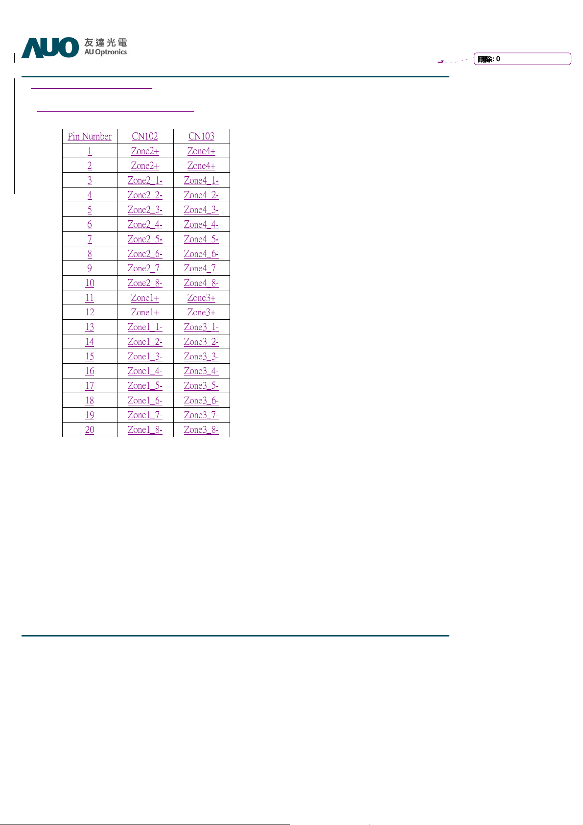
3.7.2 Input Pin Assignment
LED connector : CviLux CI1420M1HRH-NH
Pin Number
1 Zone2+ Zone4+
2 Zone2+ Zone4+
3 Zone2_1- Zone4_1-
CN102 CN103
4 Zone2_2- Zone4_2-
5 Zone2_3- Zone4_3-
6 Zone2_4- Zone4_4-
7 Zone2_5- Zone4_5-
8 Zone2_6- Zone4_6-
9 Zone2_7- Zone4_7-
10 Zone2_8- Zone4_8-
11 Zone1+ Zone3+
12 Zone1+ Zone3+
13 Zone1_1- Zone3_1-
14 Zone1_2- Zone3_2-
15 Zone1_3- Zone3_3-
16 Zone1_4- Zone3_4-
17 Zone1_5- Zone3_5-
18 Zone1_6- Zone3_6-
19 Zone1_7- Zone3_7-
20 Zone1_8- Zone3_8-
T550QVD01.0 Product Specification
Rev.2 0
刪除
刪除
刪除刪除
© Copyright AUO Optronics Corp. 2009 All Rights Reserved. Page 19 / 34
 Loading...