

AUO T460HW03 VG Specification
Global LCD Panel Exchange Center
www.panelook.com
One step solution for LCD / PDP / OLED panel application: Datasheet, inventory and accessory!
www.panelook.com
Model Name: T460HW03 VG
( )Preliminary Specifications
(****)Final Specifications
T460HW03 VG Product Specification
Rev. 1.0
Issue Date : 2010/02/08
Customer Signature Date AUO Date
Approved By
_________________________________
Note
Approval By PM Director
Frank Hsu
____________________________________
Reviewed By RD Director
Eugene Chen
____________________________________
Reviewed By Project Leader
Evan Chen
____________________________________
Prepared By PM
Ryan Chung
____________________________________
© Copyright AUO Optronics Corp. 2009 All Rights Reserved. Page 1 / 34
Global LCD Panel Exchange Center
www.panelook.com
One step solution for LCD / PDP / OLED panel application: Datasheet, inventory and accessory!
www.panelook.com
T460HW03 VG Product Specification
Rev. 1.0
Contents
No
CONTENTS
RECORD OF REVISIONS
1 GENERAL DESCRIPTION
2 ABSOLUTE MAXIMUM RATINGS
3 ELECTRICAL SPECIFICATION
3-1 ELECTRIACL CHARACTERISTICS
3-2 INTERFACE CONNECTIONS
3-3 SIGNAL TIMING SPECIFICATION
3-4 SIGNAL TIMING WAVEFORM
3-5 COLOR INPUT DATA REFERENCE
3-6 POWER SEQUENCE
3-7 BACKLIGHT SPECIFICATION
4 OPTICAL SPECIFICATION
5 MECHANICAL CHARACTERISTICS
6 RELIABILITY TEST ITEMS
7 INTERNATIONAL STANDARD
7-1 SAFETY
7-2 EMC
8 PACKING
8-1 DEFINITION OF LABEL
8-2 PACKING METHODS
8-3 PALLET AND SHIPMENT INFORMATION
9 PRECAUTION
9-1 MOUNTING PRECAUTIONS
9-2 OPERATING PRECAUTIONS
9-3 ELECTROSTATIC DISCHARGE CONTROL
9-4 PRECAUTIONS FOR STRONG LIGHT EXPOSURE
9-5 STORAGE
9-6 HANDLING PRECAUTIONS FOR PROTECT FILM
© Copyright AUO Optronics Corp. 2009 All Rights Reserved. Page 2 / 34
Global LCD Panel Exchange Center
www.panelook.com
One step solution for LCD / PDP / OLED panel application: Datasheet, inventory and accessory!
www.panelook.com
Record of Revision
T460HW03 VG Product Specification
Rev. 1.0
Version
1.0 2010/2/8 First release
Date Page Description
© Copyright AUO Optronics Corp. 2009 All Rights Reserved. Page 3 / 34
Global LCD Panel Exchange Center
www.panelook.com
One step solution for LCD / PDP / OLED panel application: Datasheet, inventory and accessory!
www.panelook.com
T460HW03 VG Product Specification
1. General Description
This specification applies to the 46 inch Color TFT-LCD Module T460HW03 VG. This LCD module has a TFT
active matrix type liquid crystal panel 1920 x 1080 pixels, and diagonal size of 46 inch. This module supports 1920
x 1080 mode with 120Hz frame rate. Each pixel is divided into Red, Green and Blue sub-pixels or dots which are
arranged in vertical stripes. Gray scale or the brightness of the sub-pixel color is determined with a 10-bit gray
scale signal for each dot.
The T460HW03 VG has been designed to apply the 10-bit 2 channel LVDS interface method. It is intended to
support displays where high brightness, wide viewing angle, high color saturation, and high color depth are very
important. The T460HW03 VG backlight unit is using inverter.
Rev. 1.0
* General Information
Items Specification Unit Note
Active Screen Size 46 inch
Display Area 1018.08(H) x 572.67(V) mm
Outline Dimension 1083.0(H) x 627.0(V) x 59.0(D) mm With Inverter
Driver Element a-Si TFT active matrix
Display Colors 10 bit, 1.07B Colors
Number of Pixels 1920 x 1080 Pixel
Pixel Pitch 0.53025 mm
Pixel Arrangement RGB vertical stripe
Display Operation Mode Normally Black
Surface Treatment Anti-Glare, 3H Haze=11%
© Copyright AUO Optronics Corp. 2009 All Rights Reserved. Page 4 / 34
Global LCD Panel Exchange Center
www.panelook.com
One step solution for LCD / PDP / OLED panel application: Datasheet, inventory and accessory!
www.panelook.com
T460HW03 VG Product Specification
2. Absolute Maximum Ratings
The followings are maximum values which, if exceeded, may cause faulty operation or damage to the unit
Item Symbol Min Max Unit Conditions
Logic/LCD Drive Voltage Vcc -0.3 14 [Volt] Note 1
Input Voltage of Signal Vin -0.3 4 [Volt] Note 1
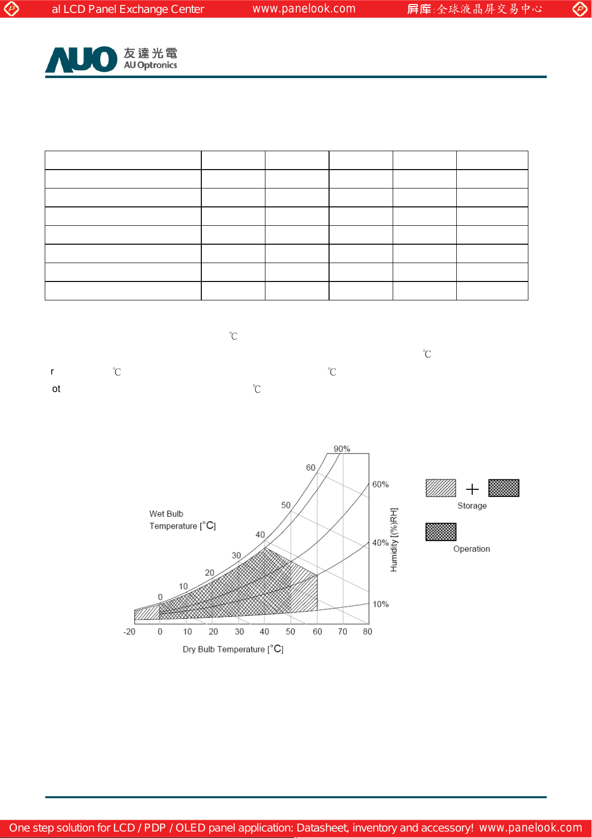
Operating Temperature TOP 0 +50 [oC] Note 2
Operating Humidity HOP 10 90 [%RH] Note 2
Storage Temperature TST -20 +60 [oC] Note 2
Storage Humidity HST 10 90 [%RH] Note 2
Panel Surface Temperature PST - 65 [oC] Note 3
Rev. 1.0
Note 1: Duration:50 msec.
Note 2 : Maximum Wet-Bulb should be 39 and No condensation.℃
The relative humidity must not exceed 90% non-condensing at temperatures of 40 or less. At temperatures
greater than 40 , the wet bulb temperature must not exceed 39 .
Note 3: Surface temperature is measured at 50℃ Dry condition
℃ ℃
℃
© Copyright AUO Optronics Corp. 2009 All Rights Reserved. Page 5 / 34
s
µ
Global LCD Panel Exchange Center
www.panelook.com
One step solution for LCD / PDP / OLED panel application: Datasheet, inventory and accessory!
www.panelook.com
T460HW03 VG Product Specification
3. Electrical Specification
The T460HW03 VG requires two power inputs. One is employed to power the LCD electronics and to drive the TFT
array and liquid crystal. The second input for BLU is to power inverter.
3.1 Electrical Characteristics
Rev. 1.0
Parameter Symbol
Unit Note
Min. Typ. Max
LCD
Power Supply Input Voltage VDD 10.8 12 13.2 VDC 1
Power Supply Input Current IDD -- 1.2 1.7 A 2
Power Consumption PC -- 14.4 20.4 Watt 2
Value
Inrush Current I
-- -- 4 A 3
RUSH
Differential Input High Threshold Voltage VTH -- -- +100 4 4
LVDS
Interface
Differential Input Low Threshold Voltage VTL -100 -- -- 4 4
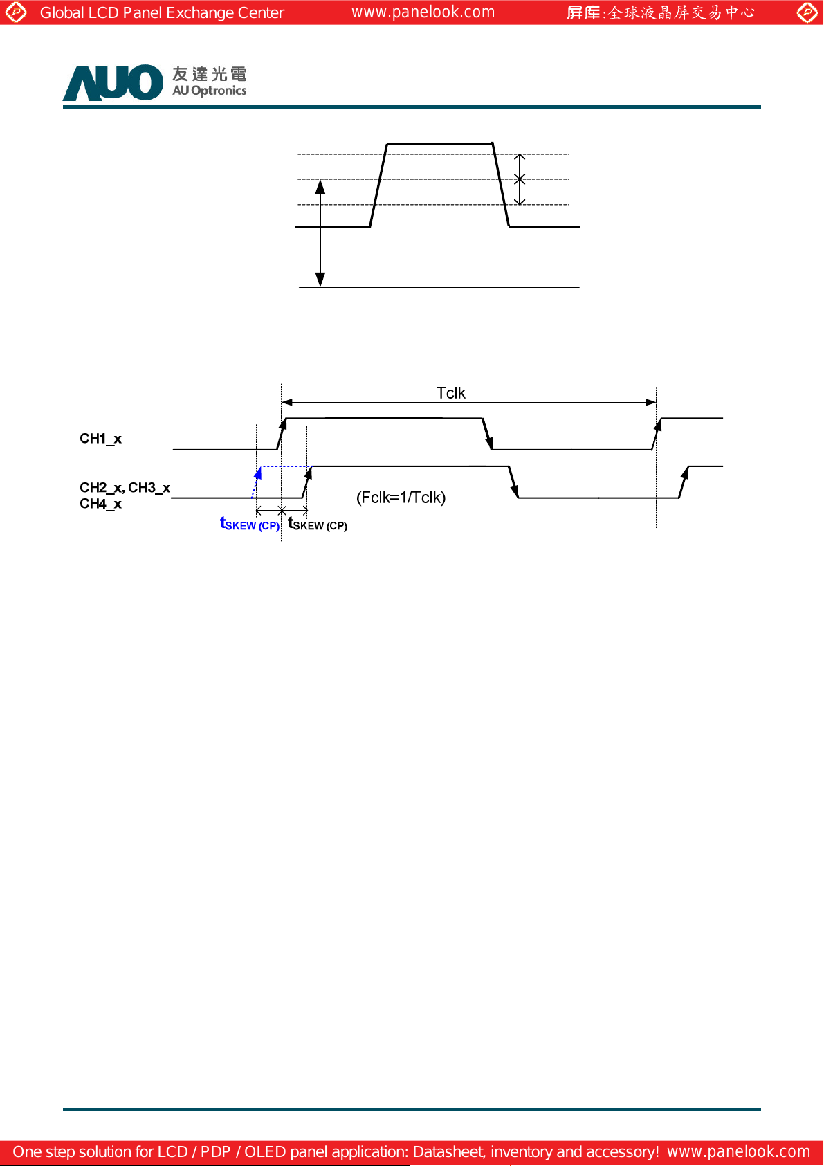
Input Common Mode Voltage V
Input Channel Pair Skew Margin t
1.10 1.25 1.40 VDC 4
ICM
SKEW (CP)
-500 -- +500 ps 5
VIH
CMOS
Interface
Input High Threshold Voltage
(High)
VIL
Input Low Threshold Voltage
(Low)
2.4 -- 3.3 VDC --
0 -- 0.6 V
--
DC
Backlight Power Consumption PBL 159.6
Life Time 50,000
Note :
1. The ripple voltage should be controlled under 10% of VCC
2. V
= 12.0V, Fv = 120Hz, F
DD
= Max freq. , 25 , Test Pattern : White Pattern℃
CLK
>> refer to “Section:3.3 Signal Timing Specification, Typical timing”
3. Measurement condition : Rising time = 400us
VVVV
DD
DD
DDDD
GND
GND
GNDGND
10%
400
400
400400
90%
168 176.4 Watt --
-- Hours
8
© Copyright AUO Optronics Corp. 2009 All Rights Reserved. Page 6 / 34
Global LCD Panel Exchange Center
www.panelook.com
One step solution for LCD / PDP / OLED panel application: Datasheet, inventory and accessory!
www.panelook.com
4. V
= 1.25V
ICM
VVVV
ICM
ICM
ICMICM
T460HW03 VG Product Specification
Rev. 1.0
VVVV
TH
TH
THTH
VVVV
TL
TL
TLTL
5. Input Channel Pair Skew Margin
0000VVVV
© Copyright AUO Optronics Corp. 2009 All Rights Reserved. Page 7 / 34
Global LCD Panel Exchange Center
www.panelook.com
One step solution for LCD / PDP / OLED panel application: Datasheet, inventory and accessory!
www.panelook.com
3.2 Interface Connections
LCD connector: 187059-51221 (P-TWO, LVDS connector)
LVDS Option for 10bit
T460HW03 VG Product Specification
Rev. 1.0
PIN Symbol Description PIN
1
2
3
4
5
6 Reserved
7
8
9
10 CH1_0- LVDS Channel 1, Signal 0- 35
11 CH1_0+ LVDS Channel 1, Signal 0+ 36
12 CH1_1- LVDS Channel 1, Signal 1- 37
13 CH1_1+ LVDS Channel 1, Signal 1+ 38
14 CH1_2- LVDS Channel 1, Signal 2- 39
15 CH1_2+ LVDS Channel 1, Signal 2+ 40
16
17 CH1_CLK-
18 CH1_CLK+
19
20 CH1_3- LVDS Channel 1, Signal 3- 45
21 CH1_3+ LVDS Channel 1, Signal 3+ 46 Reserved AUO Internal Use Only
22 CH1_4- LVDS Channel 1, Signal 4- 47 Reserved AUO Internal Use Only
23 CH1_4+ LVDS Channel 1, Signal 4+ 48 Reserved AUO Internal Use Only
24
25 CH2_0- LVDS Channel 2, Signal 0- 50 Reserved AUO Internal Use Only
VDD Power Supply, +12V DC Regulated 26
VDD Power Supply, +12V DC Regulated 27
VDD Power Supply, +12V DC Regulated 28
VDD Power Supply, +12V DC Regulated 29
VDD Power Supply, +12V DC Regulated 30
AUO Internal Use Only 31
GND Ground 32 CH2_CLK-
GND Ground 33 CH2_CLK+
GND Ground 34
GND Ground 41
LVDS Channel 1, Clock - 42 LVDS_SEL
LVDS Channel 1, Clock + 43
GND Ground 44
GND Ground 49 Reserved AUO Internal Use Only
51 FR_SELECT
Symbol Description
CH2_0+ LVDS Channel 2, Signal 0+
CH2_1- LVDS Channel 2, Signal 1-
CH2_1+ LVDS Channel 2, Signal 1+
CH2_2- LVDS Channel 2, Signal 2-
CH2_2+ LVDS Channel 2, Signal 2+
GND Ground
LVDS Channel 2, Clock -
LVDS Channel 2, Clock +
GND Ground
CH2_3- LVDS Channel 2, Signal 3-
CH2_3+ LVDS Channel 2, Signal 3+
CH2_4- LVDS Channel 2, Signal 4-
CH2_4+ LVDS Channel 2, Signal 4+
GND Ground
SCL I2C Serial Clock Bus
SDA I2C Serial Data Bus
Open/High(3.3V) for NS 8bits
Low(GND) for JEIDA 10bits
NC No connection
NC No connection
NC No connection
Input Frame Rate Selection.
High(3.3V) for 1 : 50Hz
Low/Open(GND) for 0 : 60Hz
© Copyright AUO Optronics Corp. 2009 All Rights Reserved. Page 8 / 34
Global LCD Panel Exchange Center
www.panelook.com
One step solution for LCD / PDP / OLED panel application: Datasheet, inventory and accessory!
www.panelook.com
LVDS Option = High/OpenNS
Prev iou s C ycle C urrent C ycle N e x t C ycle
Prev iou s C ycle C urrent C ycle N e x t C ycle
Prev iou s C ycle C urrent C ycle N e x t C ycle Prev iou s C ycle C urrent C ycle N e x t C ycle
Cloc k
Cloc k
Cloc kCloc k
C H x
C H x ____ 0000 ++++
C H xC H x
C H x
C H x ____ 0000 ----
C H xC H x
C H x
C H x ____ 1111 ++++
C H xC H x
C H x
C H x ____ 1111 ----
C H xC H x
T460HW03 VG Product Specification
Rev. 1.0
RRRR 0000RRRR 5555 GGGG 0000GGGG 0000RRRR 0000RRRR 1111 RRRR 2222RRRR 3333RRRR 4444 RRRR 1111
GGGG 1111BBBB 0000 BBBB 1111BBBB 1111GGGG 1111GGGG 2222 GGGG 3333GGGG 4444GGGG 5555 GGGG 2222
C H x
C H x ____ 2222 ++++
C H xC H x
C H x
C H x ____ 2222 ----
C H xC H x
C H x
C H x ____ 3333 ++++
C H xC H x
C H x
C H x ____ 3333 ----
C H xC H x
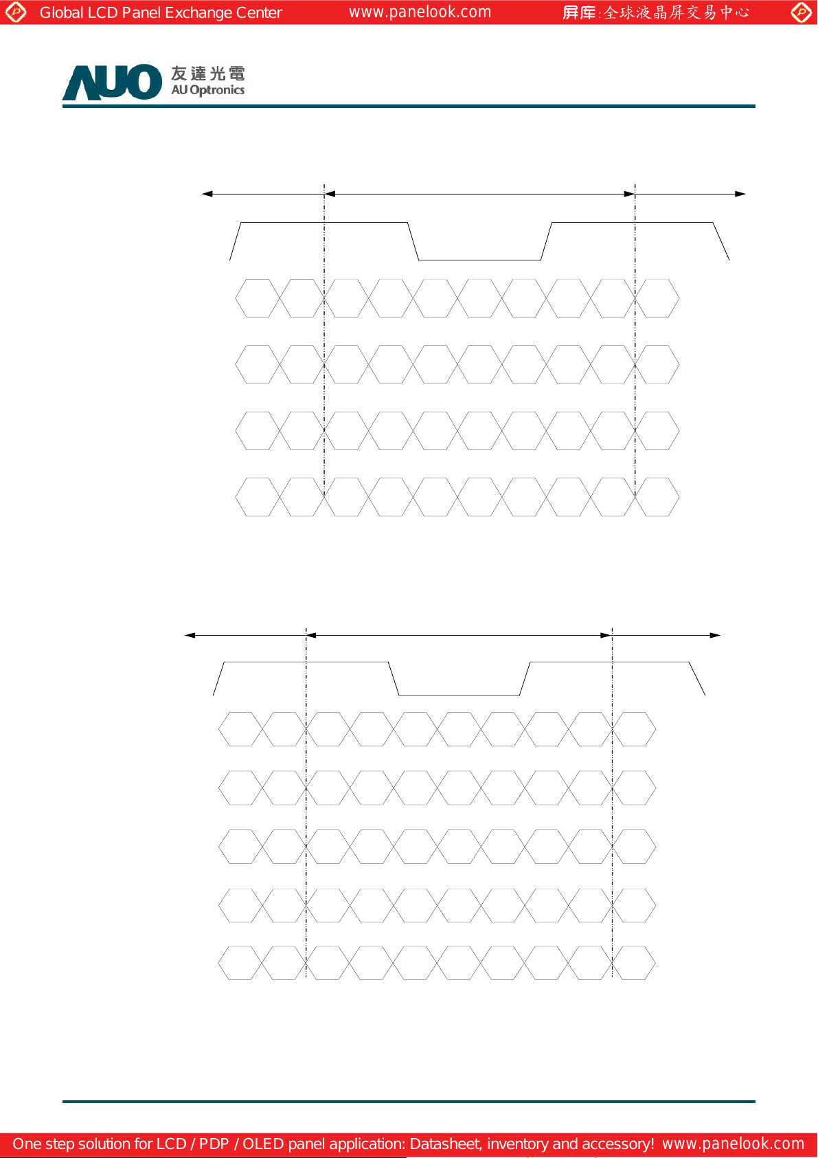
Note: x = 1, 2, 3, 4…
LVDS Option = Low/GNDJEIDA
P re vio u s C y c le C u r r e n t C y c le N e xt C y c le
P re vio u s C y c le C u r r e n t C y c le N e xt C y c le
P re vio u s C y c le C u r r e n t C y c le N e xt C y c le P re vio u s C y c le C u r r e n t C y c le N e xt C y c le
C lo ck
C lo ck
C lo ckC lo ck
C H x
C H x ____ 0000 ++++
C H xC H x
C H x
C H x ____ 0000 ----
C H xC H x
C H x
C H x ____ 1111 ++++
C H xC H x
C H x
C H x ____ 1111 ----
C H xC H x
D EBBBB 2222BBBB 3333 BBBB 4444BBBB 5555NA
D ED E
N ARRRR 6666RRRR 7777 GGGG 6666GGGG 7777BBBB 6666 RRRR 7777
N AN A
N A D E
N AN A
N A BBBB 3333
N AN A
BBBB 2222N A
RRRR 6666BBBB 7777 N A
RRRR 4444RRRR 9999 GGGG 4444GGGG 4444RRRR 4444RRRR 5555 RRRR 6666RRRR 7777RRRR 8888 RRRR 5555
GGGG 5555BBBB 4444 BBBB 5555BBBB 5555GGGG 5555GGGG 6666 GGGG 7777GGGG 8888GGGG 9999 GGGG 6666
D ED E
D ED E
N AN A
N AN A
C H x
C H x ____ 2222 ++++
C H xC H x
C H x
C H x ____ 2222 ----
C H xC H x
C H x
C H x ____ 3333 ++++
C H xC H x
C H x
C H x ____ 3333 ----
C H xC H x
C H x
C H x ____ 4444 ++++
C H xC H x
C H x
C H x ____ 4444 ----
C H xC H x
D EBBBB 6666BBBB 7777 BBBB 8888BBBB 9999N A
D ED E
N ARRRR 2222RRRR 3333 GGGG 2222GGGG 3333BBBB 2222 RRRR 3333
N AN A
N ARRRR 0000RRRR 1111 GGGG 0000GGGG 1111BBBB 0000 RRRR 1111
N AN A
N A D E
N AN A
N A BBBB 7777
N AN A
BBBB 6666N A
RRRR 2222BBBB 3333 N A
RRRR 0000BBBB 1111 N A
D ED E
D ED E
N AN A
N AN A
N AN A
N AN A
Note: x = 1, 2, 3, 4…
© Copyright AUO Optronics Corp. 2009 All Rights Reserved. Page 9 / 34
, MBR +
Global LCD Panel Exchange Center
www.panelook.com
One step solution for LCD / PDP / OLED panel application: Datasheet, inventory and accessory!
www.panelook.com
MEMC Function Description
Setting By Hardware
Pin name Content Note Default
Input Frame Rate Selection
FR_SEL
MEMC_SEL
LVDS_SEL
0: 60Hz
1: 50Hz
MEMC level selection
00: MEMC OFF
*1
01: Weak level performance
10: Middle level performance
11: Strong level performance
LVDS Format Selection
0: JEIDA Mode 10bits
1: NS Mode 8bits
1’b0
MEME OFF: 1 frame latency (~16.7ms)
MEMC ON (Weak & Middle & Strong):
10 frames latency (~170ms) for film FJC
video MBR
1’b1
T460HW03 VG Product Specification
Rev. 1.0
2’d2
I2C_SDA *2
comment
External I2C from customer's
External I2C from customer's
I2C_SCL *2
comment
Note 1.
MEMC ON/OFF can also control by external I2C. If users want to change the setting, only need to change
hardware setting or provide external I2C command. Ex: When MEMC_SEL of the hardware is 00 for MEMC OFF,
external I2C can set address=0x79 and data=0x02 for MEMC OFF.
Note 2.
The next figure shows the I2C format of customer’s single-byte command. Ex. Address : 0x65.
START 0XE4
(*1)
ACK
(*2)
Address ACK Data ACK STOP
The next figure shows the I2C format of customer’s multi-byte command. Ex. Address : 0x23.
START 0XE4 ACK
Add
ress
ACK
Data
(Byte 0)
ACK
Data
(Byte 1)
ACK
Data
(Byte 2)
ACK
Data
(Byte 3)
ACK STOP
Note (1): Slave address of MEMC chip is 0x72 plus the least significant bit indicating a write (0xE4).
Note (2): Shaded items are issued by the slave (MEMC chip).
© Copyright AUO Optronics Corp. 2009 All Rights Reserved. Page 10 / 34

corner of the OSD is from the left top corner
corner of the OSD is from the left top corner
Global LCD Panel Exchange Center
www.panelook.com
One step solution for LCD / PDP / OLED panel application: Datasheet, inventory and accessory!
www.panelook.com
Setting By External I2C
T460HW03 VG Product Specification
Rev. 1.0
Address
(Hex)
1B 0 7:0
79 0 7:0
65 0:1 15:0
59 0 7:0
23
Byte Bit Description Note Default
0:1 15:0
2:3 15:0
4:5 15:0
Output black data
0x00: unblank (normal display)
0x01: blank (output black data)
MEMC ON/OFF Selection
0x00: MEMC ON
0x02: MEMC OFF
0x04: TRUE MOVIE (5:5 pull down for
120Hz)
Control the demo option
0x0000: Demo OFF.
0x0004: Demo ON.
OSD ON/OFF control
0x00: OSD OFF
0x04: OSD ON
OSD width define
(Unit: pixel ; range 0~1920)
OSD height define
(Unit: pixel ; range 0~1080)
The amount of H pixels that the left upper
of the output window
(Unit: pixel ; range 0~1920)
The amount of V pixels that the left upper
Initial state is unblanked. 0x00
MEMC ON: 10 frames latency
(~170ms) for film FLC, MBR +
video MBR
MEME OFF: 1 frame latency
(~16.7ms)
TRUE MOVIE: latency (~80ms)
for film a frame repeat.
Demo OFF : Normal display;
Demo ON : MEMC enable at Right
side, and MEMC disable at Left
side.
OSD On/Off Control 0x00
1. OSD Protection Size Define
(Width, height, x, y)
2. Usable in OSD ON status. (The
data of address 0x59 must be
0x04.)
0x00
0x0000
0x0000
0x0000
0x0000
6:7 15:0
0 6:0
1 6:0
25
6E 0 7:0
2:4
7:0
7:0
7:0
of the output window
(Unit: pixel ; range 0~1080)
Thickness of the OSD left and right border
(Unit: pixel ; range 0~127)
Thickness of the OSD top and bottom
border (Unit: pixel ; range 0~127)
Red component of the OSD border color
Green component of the OSD border color
Blue component of the OSD border color
(Unit: 8 bit level ; range 0~255)
Different MEMC level selection
0x00: Weak 1 MEMC level (GPIO setting)
0x01: Middle MEMC level (GPIO setting)
0x02: Strong MEMC level (GPIO setting)
0x03: Weak 2 MEMC level
0x04: Weak 3 MEMC level
1. OSD border width and color
decision
2. Usable in OSD ON status. (The
data of address 0x59 must be
0x04.)
Usable in MEMC ON status. (The
data of address 0x79 must be
0x00.)
0x0000
0x00
0x00
0x00
0x00
0x00
0x01
© Copyright AUO Optronics Corp. 2009 All Rights Reserved. Page 11 / 34
 Loading...