

Page 1

Global LCD Panel Exchange Center
pecification
S
www.panelook.com
T420XW01
V
ersion June 2006
One step solution for LCD / PDP / OLED panel application: Datasheet, inventory and accessory!
www.panelook.com
Page 2
Global LCD Panel Exchange Center
COVER
CONTENTS
RECORD OF REVISIONS
GENERAL DESCRIPTION1
www.panelook.com
Contents
MNo
ITE
ABSOLUTE MAXIMUM RATINGS2
ELECTRICAL SPECIFICATIONS3
ELECTRICAL CHARACTREISTICS3-1
INTERFACE CONNECTIONS3-2
SIGNAL TIMING SPE CIFICATIONS3-3
SIGNAL TIMING WAVEFORMS3-4
COLOR INPUT DATA REFERNECE3-5
POWER SEQUENCE3-6
OPTICAL SFECIFICATIONS4
MECHAN ICAL CHARAC TERISTIC S5
6
INTERNATIONAL STANDARDS
SAFETY6-1
EMC6-2
PACKING7
PRECAUTIONS8
One step solution for LCD / PDP / OLED panel application: Datasheet, inventory and accessory!
2
www.panelook.com
Page 3
Global LCD Panel Exchange Center
V
ersion Date No Old Description New Description Remark
1.0
2005/12/23 First release
www.panelook.com
ecord of Revision
R
One step solution for LCD / PDP / OLED panel application: Datasheet, inventory and accessory!
3
www.panelook.com
Page 4
Global LCD Panel Exchange Center
General Description
1.
is specification applies to the 42 inch Color TFT-LCD Module T420XW01 V0. This LCD module has
Th
a TFT active matrix type liquid crystal panel 1366x768 pixels, and diagonal size of 42 inch. This
module supports 1366x768 WXGA mode (Non-interlace).
Each pixel is divided into Red, Green and Blue sub-pixels or dots which are arranged in vertical stripes.
Gray scale or the brightness of the sub-pixel color is determined with a 8-bit gray scale signal for each
dot.
The T420XW01 V0 has been designed to apply the 8-bit 1 channel LVDS interface method. It is
intended to support displays where high brightness, wide viewing angle, high color saturation, and
high color depth are very important.
www.panelook.com
* General Information
Items Specification Unit Note
A
ctive Screen Size 42.02 inches
splay Area 930.25(H) x 523.01(V) mm
Di
tline Dimension 983.0(H) x 576.0(V) x 54.2(D) mm With inverter
Ou
Driver Element a-Si TFT active matrix
splay Colors 16.7M Colors
Di
Number of Pixels 1366 x 768 Pixel
ixel Arrangement RGB vertical stripe
P
Display Mode Normally Black
S
urface Treatment AG, 3H
One step solution for LCD / PDP / OLED panel application: Datasheet, inventory and accessory!
4
www.panelook.com
Page 5
Global LCD Panel Exchange Center
Absolute Maximum Ratings
2.
e following are maximum values which, if exceeded, may cause faulty operation or damage to the
Th
unit.
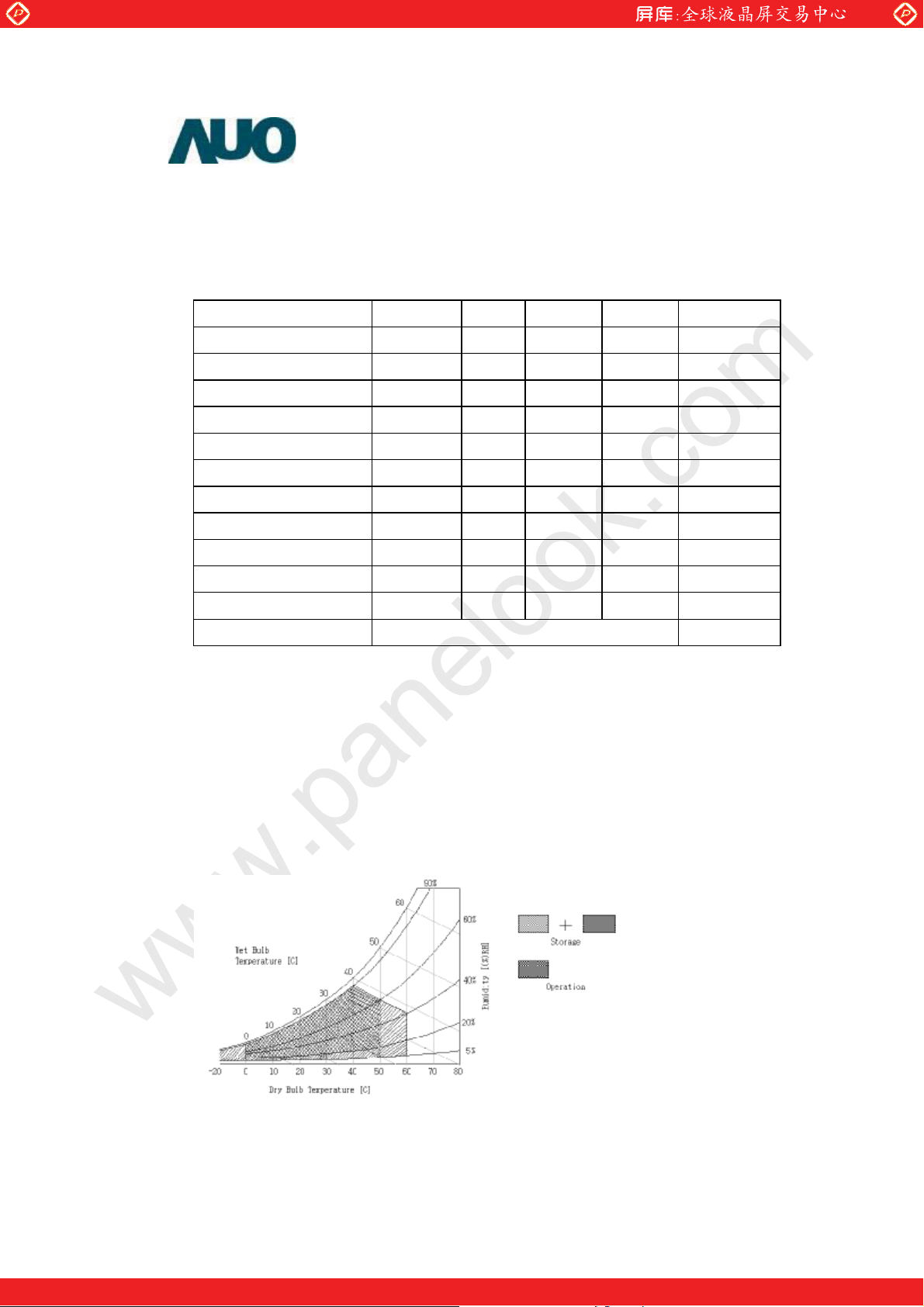
Item Symbol Min Max Unit Note
gic/LCD Drive Voltage Vdd -0.3 14.0 [Volt] 1
Lo
t Voltage of Signal Vin -0.3 3.6 [Volt] 1
Inpu
www.panelook.com
B
LU Input Voltage Vdd
BLU
Brightness Control Voltage
Opera
ting Temperature T
ting Humidity H
Opera
torage Temperature T
S
S
torage Humidity H
hock (non-operation) - 50 G 3
S
ibration (non-operation) - 1.5 G 4
V
T
hermal shock -20 60 C 5
ltitude test 50000feet (12Kpa)
A
Note 1 :
Duration = 50msec
B
-0.3
BLON -0.3
OP 0
OP
ST
ST 10
10
-2
27.0 [Volt] 1
6.0 [Volt] 1
+50 [
90 [%RH] 2
0 +60 [
90 [%RH] 2
o
C]
o
C]
2
2
Note 2 : Maximum Wet-Bulb should be 39 and No condensation.
Note 3 : Half sine wave, shock level : 50G(11ms), direction : ±x, ±y, ±z (one time each direction)
Note 4 : Wave form : random, vibration level : 1.5G RMS, Bandwidth : 10-- 300Hz
Duration : X,Y,Z 30min (one time each direction)
Note 5 : -20C/0.5hr ~ 60C/0.5hr, 10 cycles
One step solution for LCD / PDP / OLED panel application: Datasheet, inventory and accessory!
5
www.panelook.com
Page 6
Global LCD Panel Exchange Center
www.DataSheet4U.com
Electrical Specification
3.
e T420XW01 requires two power inputs. One is employed to power the LCD electronics and to drive
Th
the TFT array and liquid crystal. The second input which powers the CCFL, is typically generated by
an inverter.
-1 Electrical Characteristics
3
www.panelook.com
Para
meter Symbol
Min Typ Max
LCD:
er Supply Input Voltage Vdd 10.8 12 13.2 Vdc
Pow
er Supply Input Current Idd - TBD - A 1
Pow
er Consumption Pc - TBD - Watt 1
Pow
sh Current I
Inru
DS
LV
Interface
CM
OS
Interface
acklight Power Consumption - (170) - Watt 2
B
fferential Input
Di
High Threshold
ol
tage
Dif
ferential Input
Low Threshold
Voltage
Common Input
Voltage
Inp
ut High
Threshold Voltage
Input Low Threshold
Voltage
USH
R
VTH +100 mV
VTL -100 mV
VICM 1.10 1.25 1.40 V
VIH
(High)
VIL
(Low)
2.4 3.3 Vdc
V
alues
--
0 0.7 Vdc
TBD A 1
Unit Notes
4
4
e Time 50000 60000 Hours 3
Lif
Th
e performance of the Lamp in LCM, for example life time or brightness, is extremely influenced
by the characteristics of the DC-AC Inverter. So all the parameters of an inverter should be
carefully designed so as not to produce too much leakage current from high-voltage output of the
inverter. When you design or order the inverter, please make sure unwanted lighting caused by
the mismatch of the lamp and the inverter (no lighting, flicker, etc) never occurs. When you
One step solution for LCD / PDP / OLED panel application: Datasheet, inventory and accessory!
6
www.panelook.com
Page 7
Global LCD Panel Exchange Center
s
μ
c
onfirm it, the LCD Assembly should be operated in the same condition as installed in your
instrument.
Do not attach a conducting tape to lamp connecting wire. If the lamp wire attach to conducting
tape, TFT-LCD Module have a low luminance and the inverter has abnormal action because
leakage current occurs between lamp wire and conducting tape.
The relative humidity must not exceed 80% non-condensing at temperatures of 40or less. At
temperatures greater than 40 , the wet bulb temperature must not exceed 39 . When operate
at low temperatures, the brightness of CCFL wi ll drop and the lifetime of CCFL will be reduced.
Note :
1. Vdd=12.0V, fv=60Hz, f
www.panelook.com
CLK=
81.5 Mhz , 25, Vdd Duration time= 400
,
Test pattern : white
pattern
2. The lamp power consumption shown above does include loss of external inverter at 25.The
used lamp current is the lamp typical current
3. The life is determined as the time at which luminance of the lamp is 50% compared to that of
initial value at the typical lamp current on condition of continuous operating at 25 2.
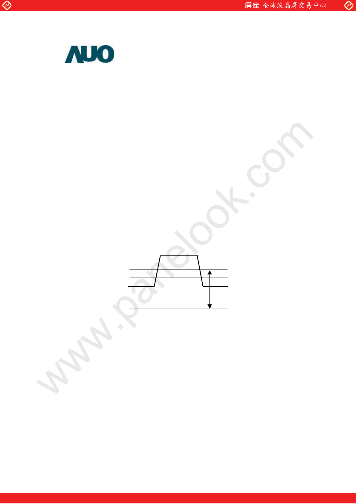
4. VICM = 1.2V
VTH
VCI
M
VTL
0V
gure : LVDS Differential Voltage
Fi
One step solution for LCD / PDP / OLED panel application: Datasheet, inventory and accessory!
7
www.panelook.com
Page 8

Global LCD Panel Exchange Center
3
-2 Interface Connections
- L
CD connector (CN1): FI-X30SSL-HF (JAE) or equivalent
-
M
ating connector: FI-30C2L (JAE) or equivalent
Pin No Symbol Description Note
1
2
3
4 VCC +12V, DC, Regulated
5
6
7
8
9
10 Reserved Open or High AUO internal test
1 GND Ground and Signal Return for LVDS
1
12
13
14
15
16
17
18
19
20 GND Ground and Signal Return for LVDS
21
22
23
24
25
26 GND Ground and Signal Return for LVDS
27
28
29
30
VCC +12V, DC, Regulated
VCC +12V, DC, Regulated
VCC +12V, DC, Regulated
GND Ground and Signal Return
GND Ground and Signal Return
GND Ground and Signal Return
GND Ground and Signal Return
LVDS Option Low/Open for Normal (NS), High for JEIDA Default : NS mode
RXIN0- LVDS Channel 0 negative
RXIN0+ LVDS Channel 0 positive
GND Ground and Signal Return for LVDS
RXIN1- LVDS Channel 1 negative
RXIN1+ LVDS Channel 1 positive
GND Ground and Signal Return for LVDS
RXIN2- LVDS Channel 2 negative
RXIN2+ LVDS Channel 2 positive
RXCLKIN- LVDS Clock negative
RXCLKIN+ LVDS Clock positive
GND Ground and Signal Return for LVDS
RXIN3- LVDS Channel 3 negative
RXIN3+ LVDS Channel 3 positive
Reserved Open or High AUO internal test
Reserved Open or High AUO internal test
GND Ground and Signal Return
GND Ground and Signal Return
www.panelook.com
One step solution for LCD / PDP / OLED panel application: Datasheet, inventory and accessory!
8
www.panelook.com
Page 9

Global LCD Panel Exchange Center
Î
Î
www.panelook.com
VDS Option = HighÎ
L
Pre
vious Cycle
Clock
RIN0+
RIN0-
RIN1+
RIN1-
RIN2+
RIN2-
IN3+
R
RIN3-
L
VDS Option = Low/OPEN
JEIDA
NS
C
urrent Cycle
N
ext Cycle
R2R7 G2G2R2R3 R4R5R6 R3
G3B2 B3B3G3G4 G5G6G6 G4
B4NA DEDEB4B5 B6B7NA B5
R0B1 NANAR0R1 G0G1B0 R1
Clock
RIN0+
RIN0-
RIN1+
RIN1-
RIN2+
RIN2-
R
IN3+
RIN3-
Previous Cycle Current Cycle Next Cycle
R0R5 G0G0R0R1 R2R3R4 R1
G1B0 B1B1G1G2 G3G4G5 G2
B2NA DEDEB2B3 B4B5NA B4
R6B7 NANAR6R7 G6G7B6 R7
One step solution for LCD / PDP / OLED panel application: Datasheet, inventory and accessory!
9
www.panelook.com
Page 10

Global LCD Panel Exchange Center
Backlight Connector Pin Configuration
1
. Electrical specification
No ITEM SYMBOL CONDITION MIN TYP MAX UNIT Note
www.panelook.com
Input Voltage V
1
2
Input Current I
Input Power P
3
Input inrush current I
4
5
Output Frequency F
/OFF Control
ON
6
Voltage
ON
/OFF Control
7
Current
xternal PWM
E
8
Control Voltage
E
xternal PWM
9
Control Current
xternal PWM Duty
E
10
Ratio
V
EV
EI
DDB
DDB
DDB
RUSH
V
BL
LON
B
OF
V
I
BLON
M
PWM
M
Max. Brightness
V
ON
FV
AX --- 2.0 --- 3.3 V
IN --- 0 --- 0.7 V
MAX PWM=100% TBD --- --- mA
PW
M
MIN PWM=100% TBD --- --- mA
ED
PW
M
---
4V
V
=2
DDB
4V
V
=2
DDB
22.8 24.0 26.4 V
TBD TBD TBD A
--- (170) TBD W 1
Dimming Max.
V
=24V
DDB
--- --- (12) A
Dimming Max.
=
24V --- 58 --- kHz
DDB
4V 2.0 --- 3.3 V
=2
DDB
24V 0.0 --- 0.7 V
=
DDB
=
24V TBD --- TBD mA
DDB
-
-- 30 --- 100 %
DC
DC
DC
DC
DC
DC
DC
1
2
DC
DC
DC
xternal PWM
E
11
Frequency
EF
PWM
Note 1 : VDIM/Open = 1.6V; PDIM = Open/High
Note 2 : Duration = 20 ms
---
120 180 300 Hz
Ta
=255, Turn on for 45minutes
One step solution for LCD / PDP / OLED panel application: Datasheet, inventory and accessory!
10
www.panelook.com
Page 11

Global LCD Panel Exchange Center
Input specification
2.
Master Board:
nnector 1: JST_S14B-PH-SM3-TB or equivalent
Co
Pin No Symbol Description
1
2
3
4
5
6
7
8
9
10
11
12
13
14
VDDB Operating Voltage Supply, +24V DC regulated
VDDB Operating Voltage Supply, +24V DC regulated
VDDB Operating Voltage Supply, +24V DC regulated
VDDB Operating Voltage Supply, +24V DC regulated
VDDB Operating Voltage Supply, +24V DC regulated
BLGND Ground and Current Return
BLGND Ground and Current Return
BLGND Ground and Current Return
BLGND Ground and Current Return
BLGND Ground and Current Return
V
DIM
(ADIM)
VBLON BL On-Off: Open/High (3.3V) for BL On as default
(2
PDIM
DIM
P
Selection
www.panelook.com
GND:
)
(1
)
)
(3
80%; Open/1.6V: 100%; High (3.3V) 120%, Luminance
External PWM/Analog Dimming Control input;
Open/High (3.3V, 100% Duty) for 100%
GND:
External PWM dimming;
Open/High: Analog dimming.
Note (1) VDIM is control signal for Inverter ’s output Power to Back Light Lamp Bulb. Input Signal
should be able to control Amplitude of Inverter Output voltage. From 0V to 3.3V, Inverter
Output Voltage should be able to vary to control Brightness of Lamp from 80% to 120%
Luminescence variation. Approx. 1.6V might be 100% Luminance control point.
Note (2) PDIM is PWM duty control Input for +3.3V TTL Level Signal. This Input Signal is Continuous
Pulse Signal with +3.3V, TTL Level Signal Spec. If this is Open or +3.3V, 100% Duty (i.e.
+3.3V, DC level), Back Light should perform 100% Luminance. Duty Ratio of this Input
signal should be proportional relationship in certain range of control without any kind of
inherent side effect like Waterfall effect on Screen. Guaranteed Duty Range and Dimming
Ratio should be specified with supplementary measurement result.
Note (3) 14 Pin is selection pin for PWM control method; if this pin is connected to GND, PDIM input
th
of 13
Open, 13
Wave Generator to generate internal PWM signal. Default setting is “Analog”, means when it
is “Not Connected”, 13
P
in should have Logic Level Duty Signal for PWM control. If this is set to High or
th
Pi
n should have DC level signal therefore the Inverter should have Saw Tooth
th
in of PWM control should be have DC Level signal for PWM.
p
One step solution for LCD / PDP / OLED panel application: Datasheet, inventory and accessory!
11
www.panelook.com
Page 12

Global LCD Panel Exchange Center
Slav
e Board:
nnector 2: JST_S12B-PH-SM3-TB or equivalent
Co
Pin No Symbol Description
www.panelook.com
1
2
3
4
5
6 BLGND Ground and Current Return
7
8
9
1
0 BLGND Ground and Current Return
11
12
VDDB Operating Voltage Supply, +24V DC regulated
VDDB Operating Voltage Supply, +24V DC regulated
VDDB Operating Voltage Supply, +24V DC regulated
VDDB Operating Voltage Supply, +24V DC regulated
VDDB Operating Voltage Supply, +24V DC regulated
BLGND Ground and Current Return
BLGND Ground and Current Return
BLGND Ground and Current Return
NC
NC
One step solution for LCD / PDP / OLED panel application: Datasheet, inventory and accessory!
12
www.panelook.com
Page 13

Global LCD Panel Exchange Center
Signal Timing Specifications
3-3
is is the signal timing required at the input of the User connector. All of the interface signal timing
Th
should be satisfied with the following specifications for it ’s proper operation.
Timing Table (DE only Mode)
Signal Item Symbol Min Type Max Unit
www.panelook.com
Period
A
ctive Tdisp (v) — 768 — Th
ertical Section
V
zontal Section
Hori
Cl
ock
ertical Frequency
V
zntal Frequency
Hori
ertical Frequency
V
Hori
zntal Frequency
LK signal input must be valid while power supply is applied.
*1) DC
*2) Display position is specific by the rise of ENAB signal only.
Horizontal display position is specified by the falling edge of 1
displayed on the left edge of the screen.
Vertical display position is specified by the rise of ENAB after a “Low” level period equivalent to eight
times of horizontal period. The 1
is displayed at the top line of screen.
3.) If a period of ENAB “High” is less than 1366 DCLK or less than 768 lines, the rest of the screen
displays black.
4.) The display position does not fit to the screen if a period of ENAB “High” and the effective data
period do not synchronize with each other.
Blanking Tblk (v) 21 54 Th
Period
A
ctive Tdisp (h) — 1366 — Tc l k
Blanking Tblk (h) 48 356 Tclk
Period
Frequency Freq 55 88 MHz
equency
Fr
equency
Fr
equency
Fr
Fr
equency
st
ta corresponding to one horizontal line after the rise the of ENAB
da
Tv 789 822 Th
Th 1414 1722 Tclk
CLK ——18.18 ns
Vs 58 60 62 Hz
Hs 4
Vs 48 50 52 Hz
Hs 3
7.34
9.45
st
DCLK
right after the rise of ENAB, is
49.3
4
1.1
2
KHz
KHz
One step solution for LCD / PDP / OLED panel application: Datasheet, inventory and accessory!
13
www.panelook.com
Page 14

Global LCD Panel Exchange Center
3-4 Signal Timing Waveforms
www.panelook.com
RGB Dat a
1366
Invalid Data
1
2
3
4
5
6
Tc
DE
Pixel
Pixel
Pi xel
Pixel
Pixel
Pix el
Pixel
Tdisp(h)
CLK
Tcl k
Th
RG
Data
B
Line
768
Invalid Data Invalid Data
Line
1
Line
2
Line
3
Li ne
4
DE
Th
Tv
Td
isp(v)
1366
Pix el
Line
768
Invalid Data
Pix el
1
Pixel
2
One step solution for LCD / PDP / OLED panel application: Datasheet, inventory and accessory!
14
www.panelook.com
Page 15

Global LCD Panel Exchange Center
3-5 Color Input Data Reference
Th
e brightness of each primary color (red, green and blue) is based on the 8 bit gray scale data input
for the color; the higher the binary input, the brighter the color. The table below provides a reference for
color versus data input.
Co
lor
MSB
LSB
www.panelook.com
CO
LOR DATA REFERENCE
I
nput Color Data
RED
MSB
LSB
GREE
N
MSB
LSB
BLUE
asic
B
Color
RE
D
EEN
GR
R7 R6 R5 R4 R3 R2 R1 R0 G7 G6 G5 G4 G3 G2 G1 G0 B7 B6 B5 B4 B3 B2 B1 B0
lack 000000000000000000000000
B
(255) 1 1 1 1 1 1 1 1 0 0 0 0000000000000
Red
n(255) 0 0 0 0 0 0 0 0 1 1 1 1111100000000
Gree
ue(255) 0 0 0 0 0 0 0 0 0 0 0 0000011111111
Bl
yan 000000001111111111111111
C
agenta 111111110000000011111111
M
ellow 111111111111111100000000
Y
White 1 1 1 1 1 1 1 1 1 1 1 1111111111111
ED(000) 0 0 0 0 0 0 0 0 0 0 0 0000000000000
R
ED(001) 0 0 0 0 0 0 0 1 0 0 0 0000000000000
R
----
ED(254) 1 1 1 1 1 1 1 0 0 0 0 0000000000000
R
RED(255) 1 1 1 1 1 1 1 1 0 0 0 0000000000000
GREEN(000) 0 0 0 0 0 0 0 0 0 0 0 0000000000000
N(001) 0 0 0 0 0 0 0 0 0 0 0 0000100000000
GREE
----
N(254) 0 0 0 0 0 0 0 0 1 1 1 1111000000000
GREE
GREEN(255) 0 0 0 0 0 0 0 0 1 1 1 1111100000000
) 000000000000000000000000
) 000000000000000000000001
-------
) 000000000000000011111110
BL
BLUE(000
BLUE(001
UE
BLUE(254
BLUE(255) 0 0 0 0 0 0 0 0 0 0 0 0000011111111
One step solution for LCD / PDP / OLED panel application: Datasheet, inventory and accessory!
15
www.panelook.com
Page 16

Global LCD Panel Exchange Center
3-6 Power Sequence
Power sequence of panel
1.
www.panelook.com
V
alues
Param
eter
t1
220-50ms
t
t3
t4
t5
t6
t7
*
: If t3=200ms, input black signal till 700ms from system is necessary. In case of t3<200ms, the
abnormal display will be happened. But it will not damage timing controller.
Apply the lamp voltage within the LCD operating range. When the backlight turns on before the LCD
operation or the LCD turns off before the backlight turns off, the display may momentarily become
abnormal.
Caut
ion : The above on/off sequence should be applied to avoid abnormal function in the display. In
case of handling, make sure to turn off the power when you plug the cable into the input connector or
pull the cable out of the connector.
Min. Typ. Max.
400 - 1000 us
700 or (200)* - - ms
200 - - ms
50 - - ms
0.47 - 30 ms
1--s
Units
One step solution for LCD / PDP / OLED panel application: Datasheet, inventory and accessory!
16
www.panelook.com
Page 17

Global LCD Panel Exchange Center
Power sequence of inverter
2.
www.panelook.com
P
ower input for Backlight
V
DDB
En
able
Back light on/off
ON)
(VBL
Dimmi
ng control signal
VDIM
DB
VD
p)
V
(Ty
DDB
V
10%
90
%
2
4V(typ.)
T1
T2 T4
p condition for Inverter
Dee
T5
90%
T3
arameter
P
alues
V
Min. Typ. Max.
T1
T2
T3
20 - - ms
500 - - ms
0- -ms
T4 1 - - ms
T5
--10ms
Units
One step solution for LCD / PDP / OLED panel application: Datasheet, inventory and accessory!
17
www.panelook.com
Page 18

Global LCD Panel Exchange Center
Optical Specification
4.
al characteristics are determined after the unit has been ‘ON’ and stable for approximately 30
Optic
minutes in a dark environment at 25. The values specified are at an approximate distance 50cm
from the LCD surface at a viewing angle of and equal to 0.
www.panelook.com
R880 or equivalent
P
ig.4-1 Optical measurement equipment and method
F
alues
V
1.3 3
8 ms 4,5 (Gray to Gray)
0
0.64
0
0.27
0
0
Typ.+0.03
0
0.15
0
0
0.28
0.290
89
89
89
89
ITE
T
l
in. Typ. Max.
M
9 p
X
meter
Para
Contras
S
Lu
Res
Color
t Ratio CR (1200) 1
urface Luminance, white LWH 400 500
minance Variation
ponse Time (Average)
Ri
se Time Tr (15) ms
ay Time Tf (5) ms
Dec
Coordinates
D R
RE
Symbo
WH
RY0.33
GRE
EN G
X
GY0.60
T
BLUE B
X
yp.-0.03
BY0.06
HITE W
W
W
ing Angle Contrast Ratio>10
View
axis, right(=0)
x
axis, left(=180)
x
y axis, up(=90)
y axis, down (=0)
X
Y
r
l
u
d
Units Notes
cd/
Degree 6
2
One step solution for LCD / PDP / OLED panel application: Datasheet, inventory and accessory!
18
www.panelook.com
Page 19

Global LCD Panel Exchange Center
3
Note:
1. Contras
t Ratio (CR) is defined mathematically as:
www.panelook.com
Contrast ratio (CR)=
Brightness on the "white" state
Brightness on the "black" state
2. Surface luminance is luminance value at point 1 across the LCD surface 50cm from the surface with
all pixels displaying white. From more information see FIG 4-2. When VDDB = 24V, IDDB = TBD.
=
Lon1, Where Lon1 is the luminance with all pixels displaying white at center 1 location.
L
WH
V/
2
6
V/
Fig
.4-2 Optical measurement point
1
7
H/
6
H
2
H/
2
3. The variation in surface luminance,WHITE is defined (center of Screen) as:
WH
ITE(9P)
=
Maximum(L
, L
,…,L
1
on
2
on
)/Mi
nimum(L
9
on
, L
,…L
1
on
2
on
)
9
on
V
Response time is the time required for the display to transition from white(L255) to black(L0) (Decay
4.
Ti me , Tr
=Tf) and from black(L0) to white(L255) (Rise Time, TrR=Tr). For additional information see
D
FIG4-3.
TrD
ig.4-3 Response time
F
TrR
One step solution for LCD / PDP / OLED panel application: Datasheet, inventory and accessory!
19
www.panelook.com
Page 20

Global LCD Panel Exchange Center
5.
The response time is defined as the following figure and shall be measured by switching the input
signal for different gray level. For additional information see FIG4-4
100%
90%
L
um inan ce
,15,L31,
L0
www.panelook.com
.L255
L0,15,L31,
.L255
10%
0%
Tr
L
0,15,L31,
D
.L255
Tr
me
Ti
R
Fig.4-4 Response time
6. Viewing angle is the angle at which the contrast ratio is greater than 10. The angles are
determined for the horizontal or x axis and the vertical or y axis with respect to the z axis which is
normal to the LCD surface. For more information see FIG4-5.
Fi
g.4-5 Viewing Angle Definition
One step solution for LCD / PDP / OLED panel application: Datasheet, inventory and accessory!
20
www.panelook.com
Page 21

Global LCD Panel Exchange Center
Mechanical Characteristics
5.
e contents provide general mechanical characteristics for the model T420XW01. In addition the
Th
figures in the next page are detailed mechanical drawing of the LCD.
Ou
tline Dimension
ezel Area
B
www.panelook.com
Horizontal (typ.) 983.0mm
ertical (typ.) 576.0mm
V
Depth (typ.) 54.2mm (with inverter)
ontal (typ.) 938.3mm
Horiz
Vertical (typ.) 531.3mm
ctive Display Area
A
Weight 15000g (typ.)
ace Treatment AG, 3H
Surf
ontal 930.25mm
Horiz
Vertical 523.01mm
One step solution for LCD / PDP / OLED panel application: Datasheet, inventory and accessory!
21
www.panelook.com
Page 22

Global LCD Panel Exchange Center
2D drawing (TBD)
www.panelook.com
One step solution for LCD / PDP / OLED panel application: Datasheet, inventory and accessory!
22
www.panelook.com
Page 23

Global LCD Panel Exchange Center
International Standard
6.
6-1. Safety
UL6500, Underwriters Laboratories, Inc. (AUO file number : E204356)
(1)
Standard for Safety of Information Technology Equipment Including electrical Business
Equipment.
(2) CAN/CSA C22.2 No. 950-95 Third Edition, Canadian Standards Association, Jan. 28, 1995
Standard for Safety of Information Technology Equipment Including Electrical Business
Equipment.
(3) EN60950 : 1992+A2: 1993+A2: 1993+C3: 1995+A4: 1997+A11: 1997
IEC 950: 1991+A1: 1992+A2: 1993+C3: 1995+A4:1996
IEC 60065
European Committee for Electro technical Standardization (CENELEC)
EUROPEAN STANDARD for Safety of Information Technology Equipment Including Electrical
Business Equipment.
www.panelook.com
6-2
. EMC
ANSI C63.4 “Methods of Measurement of Radio-Noise Emissions from Low-Voltage Electrical and
a)
Electrical Equipment in the Range of 9kHz to 40GHz. “American National standards
Institute(ANSI), 1992
b) C.I.S.P.R “Limits and Methods of Measurement of Radio Interface Characteristics of Information
Technology Equipment.” International Special committee on Radio Interference.
c) EN 55022 “Limits and Methods of Measurement of Radio Interface Characteristics of Information
Technology Equipment.” European Committee for Electrotechnical Standardization. (CENELEC),
1998
One step solution for LCD / PDP / OLED panel application: Datasheet, inventory and accessory!
23
www.panelook.com
Page 24

Global LCD Panel Exchange Center
Packing (TBD)
7.
www.panelook.com
One step solution for LCD / PDP / OLED panel application: Datasheet, inventory and accessory!
24
www.panelook.com
Page 25

Global LCD Panel Exchange Center
PRECAUTIONS
8.
e pay attention to the followings when you use this TFT LCD module.
Pleas
MOUNTING PRECAUTIONS
8-1
) You must mount a module using holes arranged in four corners or four sides.
(1
(2) You should consider the mounting structure so that uneven force (ex. Twisted stress) is not
applied to module. And the case on which a module is mounted should have sufficient strength so
that external force is not transmitted directly to the module.
(3) Please attach the surface transparent protective plate to the surface in order to protect the
polarizer. Transparent protective plate should have sufficient strength in order to the resist external
force.
(4) You should adopt radiation structure to satisfy the temperature specification.
(5) Acetic acid type and chlorine type materials for the cover case are not desirable because the
former generates corrosive gas of attacking the polarizer at high temperature and the latter causes
circuit break by electro-chemical reaction.
(6) Do not touch, push or rub the exposed polarizers with glass, tweezers or anything harder than
HB pencil lead. And please do not rub with dust clothes with chemical treatment. Do not touch the
surface of polarizer for bare hand or greasy cloth. (Some cosmetics are detrimental to the
polarizer.)
(7) When the surface becomes dusty, please wipe gently with absorbent cotton or other soft
materials like chamois soaks with petroleum benzene. Normal-hexane is recommended for
cleaning the adhesives used to attach front/ rear polarizers. Do not use acetone, toluene and
alcohol because they cause chemical damage to the polarizer.
(8) Wipe off saliva or water drops as soon as possible. Their long time contact with polarizer
causes deformations and color fading.
(9) Do not open the case because inside circuits do not have sufficient strength.
www.panelook.com
OPERATING PRECAUTIONS
8-2
The spike noise causes the mis-operation of circuits. It should be lower than following
(1)
voltage: V=200mV(Over and under shoot voltage)
(2) Response time depends on the temperature. (In lower temperature, it becomes
longer..)
(3) Brightness depends on the temperature. (In lower temperature, it becomes lower.) And
in lower temperature, response time (required time that brightness is stable after turned
on) becomes longer.
One step solution for LCD / PDP / OLED panel application: Datasheet, inventory and accessory!
25
www.panelook.com
Page 26

Global LCD Panel Exchange Center
(4)
Be careful for condensation at sudden temperature change. Condensation makes
damage to polarizer or electrical contacted parts. And after fading condensation, smear
or spot will occur.
(5) When fixed patterns are displayed for a long time, remnant image is likely to occur.
(6) Module has high frequency circuits. Sufficient suppression to the electromagnetic
interference shall be done by system manufacturers. Grounding and shielding methods
may be important to minimize the interface.
ELECTROSTATIC DISCHARGE CONTROL
8-3
nce a module is composed of electronic circuits, it is not strong to electrostatic discharge. Make
Si
certain that treatment persons are connected to ground through wrist band etc. And don ’t touch
interface pin directly.
www.panelook.com
8-4 PRECAUTIONS FOR STRONG LIGHT EXPOSURE
S
trong light exposure causes degradation of polarizer and color filter.
STORAGE
8-5
W
hen storing modules as spares for a long time, the following precautions are necessary.
(1) Store them in a dark place. Do not expose the module to sunlight or fluorescent light. Keep the
temperature between 5and 35at normal humidity.
(2) The polarizer surface should not come in contact with any other object. It is recommended that
they be stored in the container in which they were shipped.
8-6 HANDLING PRECAUTIONS FOR PROTECTION FILM
The protection film is attached to the bezel with a small masking tape. When the protection film is
(1)
peeled off, static electricity is generated between the film and polarizer. This should be peeled off
slowly and carefully by people who are electrically grounded and with well ion-blown equipment or
in such a condition, etc.
(2) When the module with protection film attached is stored for a long time, sometimes there remains
a very small amount of flue still on the Bezel after the protection film is peeled off.
(3) You can remove the glue easily. When the glue remains on the Bezel or its vestige is recognized,
please wipe them off with absorbent cotton waste or other soft material like chamois soaked with
normal-hexane.
One step solution for LCD / PDP / OLED panel application: Datasheet, inventory and accessory!
26
www.panelook.com
 Loading...