

Page 1
Global LCD Panel Exchange Center
www.panelook.com
©Copyrig ht AU Optronics Corp.
2009 All Rights Reserved. T420HW04 V6 0/31
No Reproduction and Redistribution Allowed
One step solution for LCD / PDP / OLED panel application: Datasheet, inventory and accessory!
www.panelook.com
Page 2
Global LCD Panel Exchange Center
www.panelook.com
Document Version: 2.0
Date: 2009/8/19
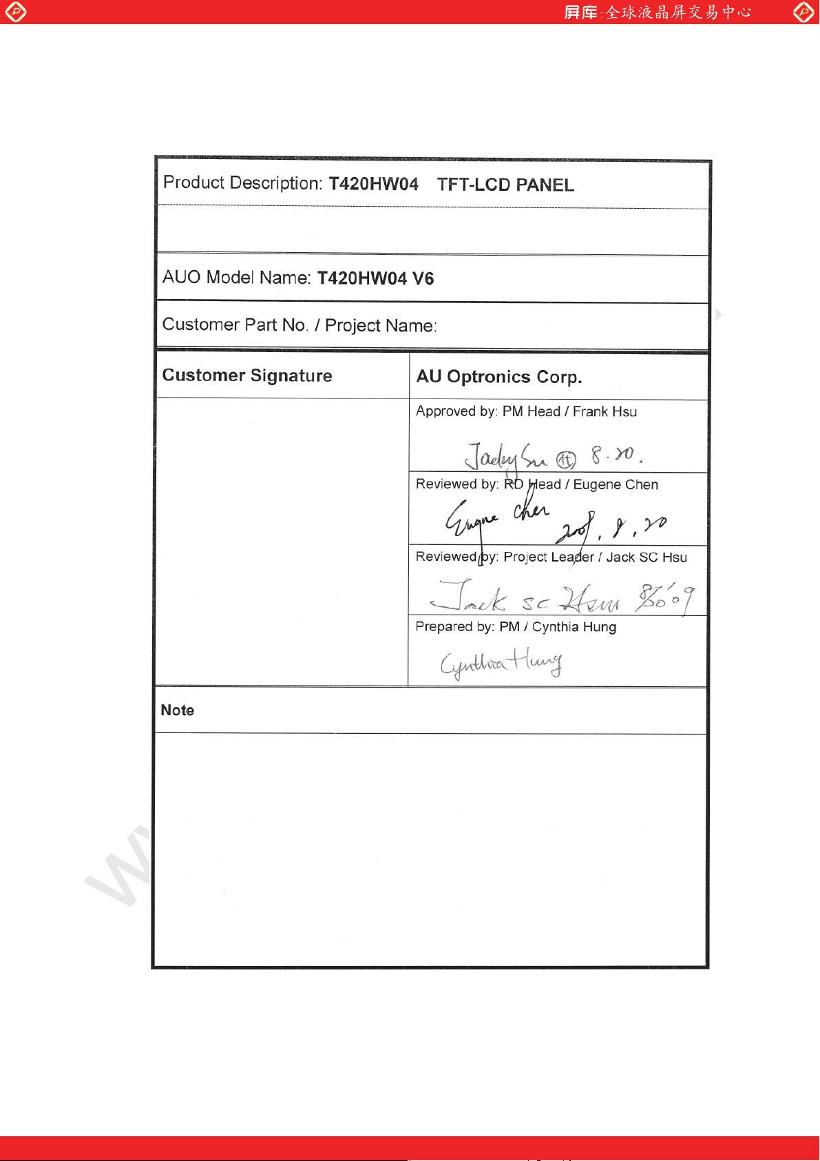
Product Functional Specification
42” Full HD Color TFT-LCD Module
Model Name: T420HW04 V6
() Preliminary Specification
(*) Final Specification
©Copyrig ht AU Optronics Corp.
2009 All Rights Reserved. T420HW04 V6 1/31
No Reproduction and Redistribution Allowed
One step solution for LCD / PDP / OLED panel application: Datasheet, inventory and accessory!
www.panelook.com
Page 3
Global LCD Panel Exchange Center
No
CONTENTS
RECORD OF REVISIONS
1 GENERAL DESCRIPTION
2 ABSOLUTE MAXIMUM RATINGS
3 ELECTRICAL SPECIFICATION
3-1 ELECTRIACL CHARACTERISTICS
3-2 INTERFACE CONNECTOR
www.panelook.com
Contents
3-3 SIGNAL TIMING SPECIFICATION
3-4 SIGNAL TIMING WAVEFORM
3-5 COLOR INPUT DATA REFERENCE
3-6 POWER SEQUENCE
3-7 BACK LIGHT POWER SPECIFICATION
4 OPTICAL SPECIFICATION
5 MECHANICAL CHARACTERISTICS
6 Reliability
7 INTERNATIONAL STANDARD
8 PACKING
9 PRECAUTION
©Copyrig ht AU Optronics Corp.
2009 All Rights Reserved. T420HW04 V6 2/31
No Reproduction and Redistribution Allowed
One step solution for LCD / PDP / OLED panel application: Datasheet, inventory and accessory!
www.panelook.com
Page 4
Global LCD Panel Exchange Center
Record of Revision
Version Data Page. Old Description New Description Remark
1.0 2009/6/26 - Preliminary spec first release
2.0 2009/08/19 13 Update Tv max =1200
www.panelook.com
©Copyrig ht AU Optronics Corp.
2009 All Rights Reserved. T420HW04 V6 3/31
No Reproduction and Redistribution Allowed
One step solution for LCD / PDP / OLED panel application: Datasheet, inventory and accessory!
www.panelook.com
Page 5
Global LCD Panel Exchange Center
1. General Description
This specification applies to the 42 inch Color TFT-LCD Module T420HW04 V6. This LCD module has
a TFT active matrix type liquid crystal panel 1920x1080 pixels, and diagonal size of 42 inch. This
module supports Full HD mode (Non-interlace).
Each pixel is divided into Red, Green and Blue sub-pixels or dots which are arranged in vertical stripes.
Gray scale or the brightness of the sub-pi xel color is determined with a 8-bit gray scale signal for each
dot.
The T420HW04 V6 has been designed to apply the 8-bit 2 channel LVDS interface method. It is
intended to support displays where high brightness, EBU Gamut (72% NTSC), wide viewing angle,
and high color depth are very important. The T420HW04 V6 backlight unit is using inverter solution.
www.panelook.com
* General Information
Items Specification Unit Note
Active Screen Size 42.02 inches
Display Area 930.24(H) x 523.26(V) mm
Outline Dimension 983.0(H) x 576.0(V) x 52.5(D) mm With inverter
Driver Element a-Si TFT active matrix
Display Colors 1073.7M Colors
Color Gamut 72 % NTSC
Number of Pixels 1920 x 1080 Pixel
Pixel Pitch 0.4845 mm
Pixel Arrangement RGB vertical stripe
Display Mode Normally Black
Lamp quantity, type 16pcs, Straight type pcs
Surface Treatment Anti-Glare coating (Haze 11%)
Hard coating (3H)
©Copyrig ht AU Optronics Corp.
2009 All Rights Reserved. T420HW04 V6 4/31
No Reproduction and Redistribution Allowed
One step solution for LCD / PDP / OLED panel application: Datasheet, inventory and accessory!
www.panelook.com
Page 6
Global LCD Panel Exchange Center
2. Absolute Maximum Ratings
The followings are maximum values which, if exceeded, may cause faulty operation or damage to the
unit
Item Symbol Min. Max Unit Note
www.panelook.com
Logic/LCD Drive Voltage V
Input Voltage of Signal V
Operating Temperature T
Operating Humidity H
Storage Temperature T
Storage Humidity H
Panel Surface Temperature T
DD
IN
OP
OP
ST
ST
SUR
-0.3 14.0 V
-0.3 4 V
DC
DC
1
1
0+50 °C2
10 80 %RH 2
-20 +60 °C2
10 80 %RH 2
-- +65 °C2
Shock (non-operation) ±x, ±y-- 50 G 3
Shock (non-operation) ±z--50 G 3
Vibration (non-operation) -- 1.5 G 4
Note 1: Duration = 50ms
Note 2: Maximum Wet-Bulb should be 39°C and no condensation. The relative humidity must
not exceed 90% non-condensing at temperatures of 40 °C or less. At temperatures
greater than 40°C, the wet bulb temperature must not exceed 39°C.
Note 3: Sine wave, 11ms, direction: ±x, ±y, ±z (one time each direction)
Note 4: Wave form: random, vibration level: 1.5G RMS, Bandwidth: 10--300Hz
Duration: X, Y, Z 30min (one time each direction)
80%
©Copyrig ht AU Optronics Corp.
2009 All Rights Reserved. T420HW04 V6 5/31
No Reproduction and Redistribution Allowed
One step solution for LCD / PDP / OLED panel application: Datasheet, inventory and accessory!
www.panelook.com
Page 7

Global LCD Panel Exchange Center
3. Electrical Specification
The T420HW04 V6 requires two power inputs. One is employed to power the LCD electronics and to
drive the TFT array and liquid crystal. The second input, w hich powers the CCFL, is typically
generated by an integrate power (I/P) system.
3.1 Electrical Characteristics
Parameter Symbol
www.panelook.com
Val ue
Unit Note
Min. Typ. Max
Power Supply Input Voltage V
Power Supply Input Current I
Power Consumption P
Inrush Current I
DD
DD
C
RUSH
10.8 12 13.2 V
1 1.3 A 1
4A5
DC
Watt 1
Differential Input
High Threshold
V
TH
+100 mV
DC
Voltage
LVDS
Interface
Differential Input
Low Threshold
V
TL
-100 mV
DC
Voltage
Common Input
Voltage
Input High
CMOS
Interface
Threshold Voltage
Input Low
Threshold Voltage
Backlight Power Consumption (ref.) P
V
CIM
V
IH
(High)
V
IL
(Low)
BL
0.6 1.2 1.8 V
2.0 3.3 V
0 0.8 V
DC
DC
DC
Watt 2
Life Time 50000 -- -- Hours 3
4
4
The performance of the Lamp in LCD panel, for example life time or brightness, is extremely
influenced by the characteristics of the balance board and I/P board. All the parameters should be
carefully designed as not to produce too much leakage current from high-voltage output. While
design or order balance board, please make sure unwanted lighting caused by the mismatch of
the lamp and balance board (no lighting, flicker, etc) never occurs. After confirmation, the LCD
Panel should be operated in the same condition as installed in your instrument.
©Copyrig ht AU Optronics Corp.
2009 All Rights Reserved. T420HW04 V6 6/31
No Reproduction and Redistribution Allowed
One step solution for LCD / PDP / OLED panel application: Datasheet, inventory and accessory!
www.panelook.com
Page 8
Global LCD Panel Exchange Center
s
μ
Do not attach a conducting tape to lamp connecting wire. If the lamp wire attach to conducting
tape, TFT-LCD Module has a low luminance and the inverter has abnormal action, because
leakage current occurs between lamp wire and conducting tape.
When operate at low temperatures, the brightness of CCFL will drop and the lifetime of CCFL will
be reduced.
Note:
1. V
2. The backlight power consumption shown above is tested by lamp current I
3. The life is determined as the time at which luminance of the lamp is 50% compared to that of
4. V
=12.0V, fV=60Hz, fCLK=74.25Mhz, 25°C, VDDduration time=400µs, test pattern: w hite
DD
pattern
initial value at the typical lamp current on condition of continuous operating at 25 ±2°C.
=1.20V
CIM
www.panelook.com
=7.6mA.
L
VTH
VCIM
VTL
0V
Figure: LVDS Differential Voltage
5. Measurement condition: rising time=400µs
GND
0.1 Vdd
400
0.9 Vdd
Vdd
©Copyrig ht AU Optronics Corp.
2009 All Rights Reserved. T420HW04 V6 7/31
No Reproduction and Redistribution Allowed
One step solution for LCD / PDP / OLED panel application: Datasheet, inventory and accessory!
www.panelook.com
Page 9

Global LCD Panel Exchange Center
3.2 Interface Connections
LCD connector 1 : P-TWO 187059-5122 which is compatible FI-RE51S-HF (JAE)
PIN # Signal Name Description
www.panelook.com
1 V
2 V
3 V
4 V
5 V
DD
DD
DD
DD
DD
Operating voltage supply, +12V DC regulated
Operating voltage supply, +12V DC regulated
Operating voltage supply, +12V DC regulated
Operating voltage supply, +12V DC regulated
Operating voltage supply, +12V DC regulated
6 GND Ground
7 GND Ground
8 GND Ground
9 GND Ground
10 RO_0- LVDS Channel 1, pair 0, negative
11 RO_0+ LVDS Channel 1, pair 0, positive
12 RO_1- LVDS Channel 1, pair 1, negative
13 RO_1+ LVDS Channel 1, pair 1, positive
14 RO_2- LVDS Channel 1, pair 2, negative
15 RO_2+ LVDS Channel 1, pair 2, positive
16 GND Ground
17 RO_CLK- LVDS Clock, Channel 1, negative
18 RO_CLK+ LVDS Clock, Channel 1, positive
19 GND Ground
20 RO_3- LVDS Channel 1, pair 3, negative
21 RO_3+ LVDS Channel 1, pair 3, positive
22 RO_4- LVDS Channel 1, pair 4, negative
23 RO_4+ LVDS Channel 1, pair 4, positive
24 GND Ground
25 RE_0- LVDS Channel 2, pair 0, negative
26 RE_0+ LVDS Channel 2, pair 0, positive
27 RE_1- LVDS Channel 2, pair 1, negative
28 RE_1+ LVDS Channel 2, pair 1, positive
29 RE_2- LVDS Channel 2, pair 2, negative
30 RE_2+ LVDS Channel 2, pair 2, positive
31 GND Ground
32 RE_CLK- LVDS Clock, Channel 2, negative
33 RE_CLK+ LVDS Clock, Channel 2, positive
©Copyrig ht AU Optronics Corp.
2009 All Rights Reserved. T420HW04 V6 8/31
No Reproduction and Redistribution Allowed
One step solution for LCD / PDP / OLED panel application: Datasheet, inventory and accessory!
www.panelook.com
Page 10
Global LCD Panel Exchange Center
34 GND Ground
35 RE_3- LVDS Channel 2, pair 3, negative
36 RE_3+ LVDS Channel 2, pair 3, positive
37 RE_4- LVDS Channel 2, pair 4, negative
38 RE_4+ LVDS Channel 2, pair 4, positive
39 GND Ground
40 NC (reserved) No Connection (AUO internal use)
41 NC (reserved) No Connection (AUO internal use)
42 NC (reserved) No Connection (AUO internal use)
43 NC (reserved) No Connection (AUO internal use)
44 MEMC_ON
45 LVDS_FORMAT
www.panelook.com
MEMC ON/OFF Selection
Low: MEMC OFF
High/Open: MEMC ON
LVDS Format Selection
Low: Support JEIDA Mode 10/8bits
High/Open: Support NS Mode 8bits
46 SCL_E External I2C from customer's comment
47 NC (reserved) No Connection (AUO internal use)
48 SDA_E External I2C from customer's comment
49 NC (reserved) No Connection (AUO internal use)
50 NC (reserved) No Connection (AUO internal use)
51 NC (reserved) No Connection (AUO internal use)
Note 1: All GND (ground) pins should be connected together and should also be connected to
the LCD’s metal frame.
Note 2: All V
Note 3: All NC (no connection) pins should be open without voltage input.
(power input) pins should be connected together.
DD
©Copyrig ht AU Optronics Corp.
2009 All Rights Reserved. T420HW04 V6 9/31
No Reproduction and Redistribution Allowed
One step solution for LCD / PDP / OLED panel application: Datasheet, inventory and accessory!
www.panelook.com
Page 11
Global LCD Panel Exchange Center
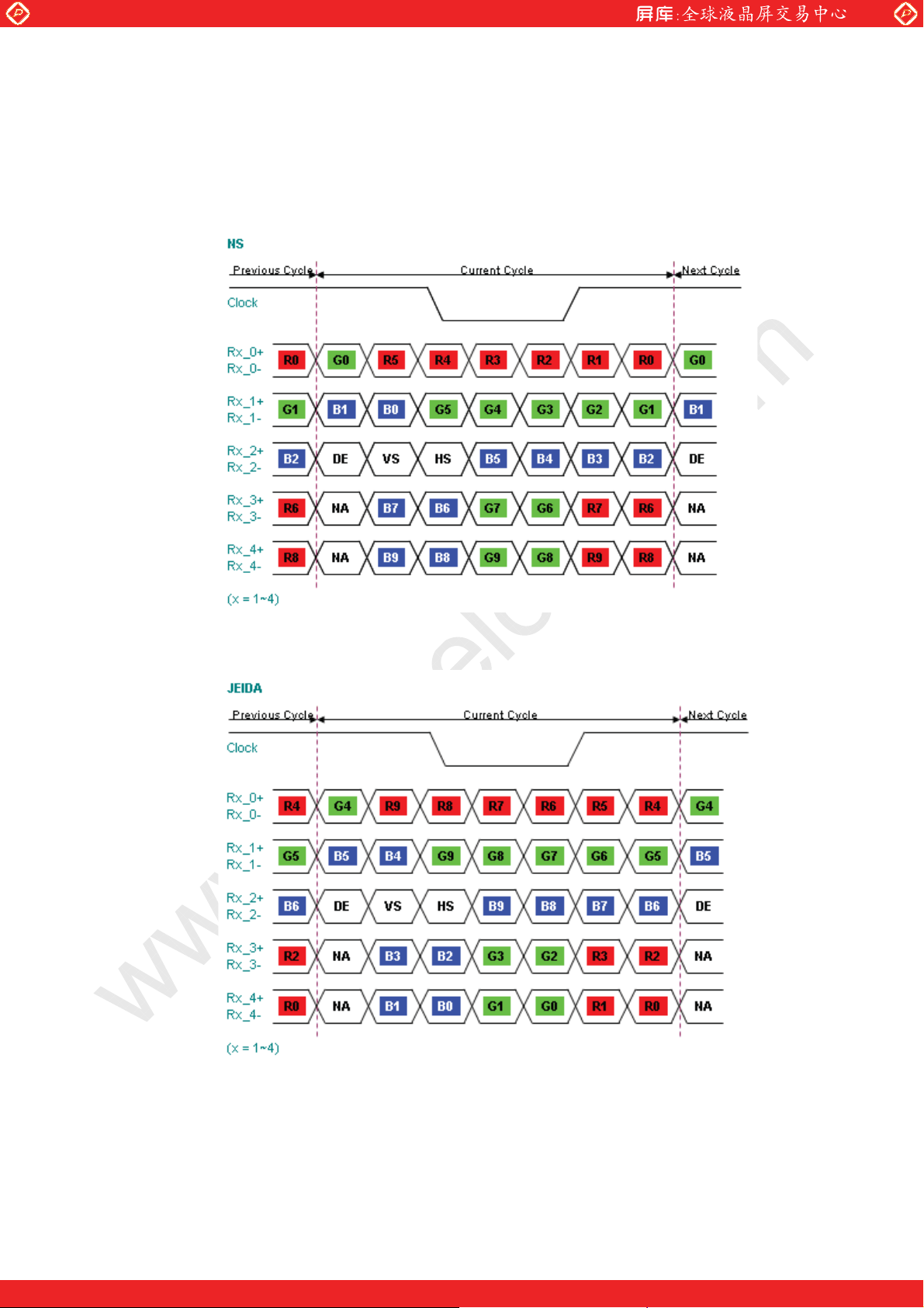
LVDS Option = High/Open NS
www.panelook.com
(X = O E)
LVDS Option = Low JEIDA
(X = O E)
©Copyrig ht AU Optronics Corp.
2009 All Rights Reserved. T420HW04 V6 10/31
No Reproduction and Redistribution Allowed
One step solution for LCD / PDP / OLED panel application: Datasheet, inventory and accessory!
www.panelook.com
Page 12
Global LCD Panel Exchange Center
MEMC function description
1. Setting by hardware
Input/
Pin na m e
ouptut
ME MC _ O N * 1 I
LVDS_FORMAT I
SDA_MCU I/OInternal I2C to c o n tro l ME MC
SCL_MCU I/O Internal I2C to c o n tr o l ME MC
www.panelook.com
Content Note
MEMC ON/OFF Selection
0: MEMC OFF
1: MEMC ON
LVDS Forma t Selection
0: J E I DA Mode 10/8bits
1: NS Mode 8bits
MEMC ON: 10 frames latency (~170ms) for
film FLC, MBR + video MBR
MEME OFF: 1 frame latency (~16.7ms)
Default
1
1
1
External I2C from cus tomer's
When MC U gets external I2C signals from
SDA_E *2 I/O
comment
cus t omer's comment,MCUwill d own load
register setting fo r ME MC chip by
External I2C from cus tomer's
SCL_E *2 I/O
MC U _ S D A and MC U _S C L . T he shee t of
comment
reg ister map s hows detail register setting.
Note 1.
MEMC ON/OFF can also control by external I2C. If users want to change the setting, only need to
change hardware setting or provide external I2C command. Ex: When MEMC_ON of the hardware is L
for MEMC OFF, external I2C can set address=0x79 and data=0x00 for MEMC ON.
Note 2.
The next figure shows the I2C format of customer’s single-byte command. Ex. Address : 0x65.
START 0XE4
(*1)
ACK
(*2)
Address ACK Data ACK STOP
(*3)
The next figure shows the I2C format of customer ’s multi-byte command. Because of MCU buffer
capacity multi-byte command has 20 bytes limitation per one time. Ex. Address : 0x23.
STAR T 0XE4 ACK
Add
ress
ACK
Data
(Byte 0)
ACK
Data
(Byte 1)
ACK
Data
(Byte 2)
ACK
Data
(Byte 3)
ACK
Note (1)
Slave address of MEMC chip is 0x72 plus the least significant bit indicating a write (0xE4).
Note (2)
Shaded items are issued by the slave (MEMC chip).
Note (3)
The interval time between the two commands must longer than 100ms.
1
STOP
(*3)
©Copyrig ht AU Optronics Corp.
2009 All Rights Reserved. T420HW04 V6 11/31
No Reproduction and Redistribution Allowed
One step solution for LCD / PDP / OLED panel application: Datasheet, inventory and accessory!
www.panelook.com
Page 13

Global LCD Panel Exchange Center
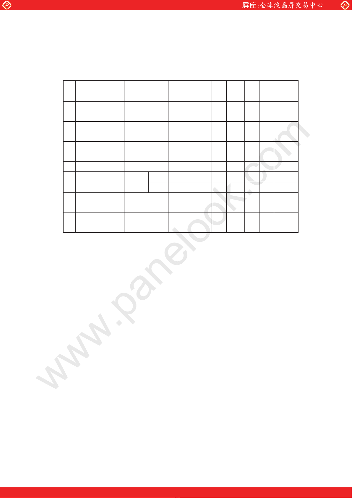
2. Setting by External I2C
www.panelook.com
Address
(Hex)
Byte Bit Description Note Default
1B 0 7:0
79 0 7:0
65 0:1 15:0
59 0 7:0
0:1 15:0
2:3 15:0
23
4:5 15:0
6:7 15:0
Output black data
0x00: unblank (normal display)
0x01: blank (output black data)
MEMC ON/OFF Selection
0x00: MEMC ON
0x02: MEMC OFF
Control the demo option
0x0000: Demo OFF.
0x0004: Demo ON.
OSD ON/OFF control
0x00: OSD OFF
0x04: OSD ON
OSD width define
(Unit: pixel ; range 0~1920)
OSD height define
(Unit: pixel ; range 0~1080)
The amount of H pixels that the left upper
corner of the OSD is from the left top corner
of the ou
(Unit: pixel ; range 0~1920)
The amount of V pixels that the left upper
corner of the OSD is from the left top corner
of the output window
(Unit: pixel ; range 0~1080)
tput window
Initial state is unblanked. 0x00
MEMC ON: 10 frames latency
(~170ms) for film FLC, MBR +
video MBR
MEME OFF: 1 frame latency
(~16.7ms)
Demo OFF : Normal display;
Demo ON : MEMC enable at
Left side, and MEMC disable at
right side.
OSD On/Off Control 0x00
1. OSD Protection Size Define
(Width, height, x, y)
2. Usable in OSD ON status.
(The data of address 0x59 must
be 0x04.)
0x00
0x0000
0x0000
0x0000
0x0000
0x0000
25
©Copyrig ht AU Optronics Corp.
2009 All Rights Reserved. T420HW04 V6 12/31
No Reproduction and Redistribution Allowed
0 6:0
1 6:0
2:4
Thickness of the OSD left and right border
(Unit: pixel ; range 0~127)
Thickness of the OSD top and bottom
border (Unit: pixel ; range 0~127)
Red component of the OSD border color
7:0 0x00
Green component of the OSD border color
7:0
1. OSD border width and color
decision
2. Usable in OSD ON status.
(The data of address 0x59 must
be 0x04.)
One step solution for LCD / PDP / OLED panel application: Datasheet, inventory and accessory!
0x00
0x00
0x00
www.panelook.com
Page 14

Global LCD Panel Exchange Center
7:0
6E 0 7:0
3.3 Signal Timing Specification
This is the signal timing required at the input of the user connector. All of the interface signal timing
should be satisfied with the following specifications for its proper operation.
Timing Table
Vertical Frequency Range (60Hz)
www.panelook.com
Blue component of the OSD border color
(Unit: 8 bit level ; range 0~255)
Different MEMC level selection
0x00: Normal MEMC level
0x01: Strong MEMC level
0x03: Weak MEMC level
Usable in MEMC ON status.
(The data of address 0x79 must
be 0x00.)
0x00
0x00
Signal Item Symbol Min. Typ. Max Unit
Period T
Vertical Section
Active T
Blanking T
DISP
BLK
Front porch Tfp(V) 1 4 110 T
Back porch Tbp(V) 1 36 110 T
V_sync
TVsync_wdth 2 5 110 T
Period T
Active T
Blanking T
Horizontal Section
DISP
BLK
Front porch Tfp(H) 5 44 180 T
Back porch T(H) 5 74 180 T
H_sync THsync_wdth
Period T
Clock
Frequency F
Vertical Frequency Frequency F
Horizontal Frequency Frequency F
V
1100 1125 1200 T
(V) 1080 T
(V) 20 45 120 T
H
1050 1100 1150 T
(H) 960 T
(H) 90 140 190 T
5 22 180 T
CLK
CLK
70.875 74.25 76 MHz
V
H
59.5 60 60.5 Hz
65.64 67.5 72 KHz
13.47 ns
H
H
H
H
H
H
CLK
CLK
CLK
CLK
CLK
CLK
Note 1: T
(V) = Tfp(V) + TVsync_wdth + Tbp(V)
BLK
T
(H) = Tfp(H) + THsync_wdth + T(H)
BLK
©Copyrig ht AU Optronics Corp.
2009 All Rights Reserved. T420HW04 V6 13/31
No Reproduction and Redistribution Allowed
One step solution for LCD / PDP / OLED panel application: Datasheet, inventory and accessory!
www.panelook.com
Page 15

Global LCD Panel Exchange Center
3.4 Signal Timing Waveforms
DE
www.panelook.com
Tv
Tblk(v )Tdisp(v )
Th
RGB Data
(ODD)
CLK
DE
RGB Data
(ODD)
RGB Data
(EV E N)
Hsync
DE
TH(sync_width)
Invalid data
TCLK
Th
Tblk(h )
Th
Tfp(h) Tbp(h)
Tdisp(h )
Tdisp(h)
TV(sync_width)
Vsync
DE
©Copyrig ht AU Optronics Corp.
2009 All Rights Reserved. T420HW04 V6 14/31
No Reproduction and Redistribution Allowed
One step solution for LCD / PDP / OLED panel application: Datasheet, inventory and accessory!
www.panelook.com
Page 16

Global LCD Panel Exchange Center
3.5 Color Input Data Reference
The brightness of each primary color (red, green and blue) is based on the 10 bit gray scale data input
for the color; the higher the binary input, the brighter the color. The table below provides a reference for
color versus data input.
www.panelook.com
COLOR DATA REFERENCE
Input Color Data
Color
Black 00000000000000 0000000000000000
Red(1023) 1 111111111 00000 000000000000000
Green(1023) 0000000000111 11111110000000000
Basic
Blue(1023) 0 00000000000 00 0000001111111111
Color
Cyan 00000000001 1111111111111111111
Magenta 1 11111111100000 000001111111111
Yellow 11111111111 111 1111110000000000
White 1 11111111111111111111111111111
RED(000) 0 00000000000000000000000000000
RED(001) 0 00000000100000000000000000000
RED
GREEN
----
RED(1022) 111111111000000000000000000000
RED(1023) 111111111100000000000000000000
GREEN(000) 0000000000 00000 000000000000000
GREEN(001) 0000000000 00000 000010000000000
----
MSB LSB
R9 R8 R7 R6 R5 R4 R3 R2 R1 R0 G9 G8 G7 G6 G5 G4 G3 G2 G1 G0 B9 B8 B7 B6 B5 B4 B3 B2 B1 B0
RED
MSB LSB
GREEN
BLUE
MSB LSB
GREEN(1022)00000000001111 1111100000000000
GREEN(1023)00000000001111 1111110000000000
BLUE(000) 00000000000 000 0000000000000000
BLUE(001) 00000000000 000 0000000000000001
BLUE
-------
BLUE(1022) 0 000000000 00000 000001111111110
BLUE(1023) 0 000000000 00000 000001111111111
©Copyrig ht AU Optronics Corp.
2009 All Rights Reserved. T420HW04 V6 15/31
No Reproduction and Redistribution Allowed
One step solution for LCD / PDP / OLED panel application: Datasheet, inventory and accessory!
www.panelook.com
Page 17
Global LCD Panel Exchange Center
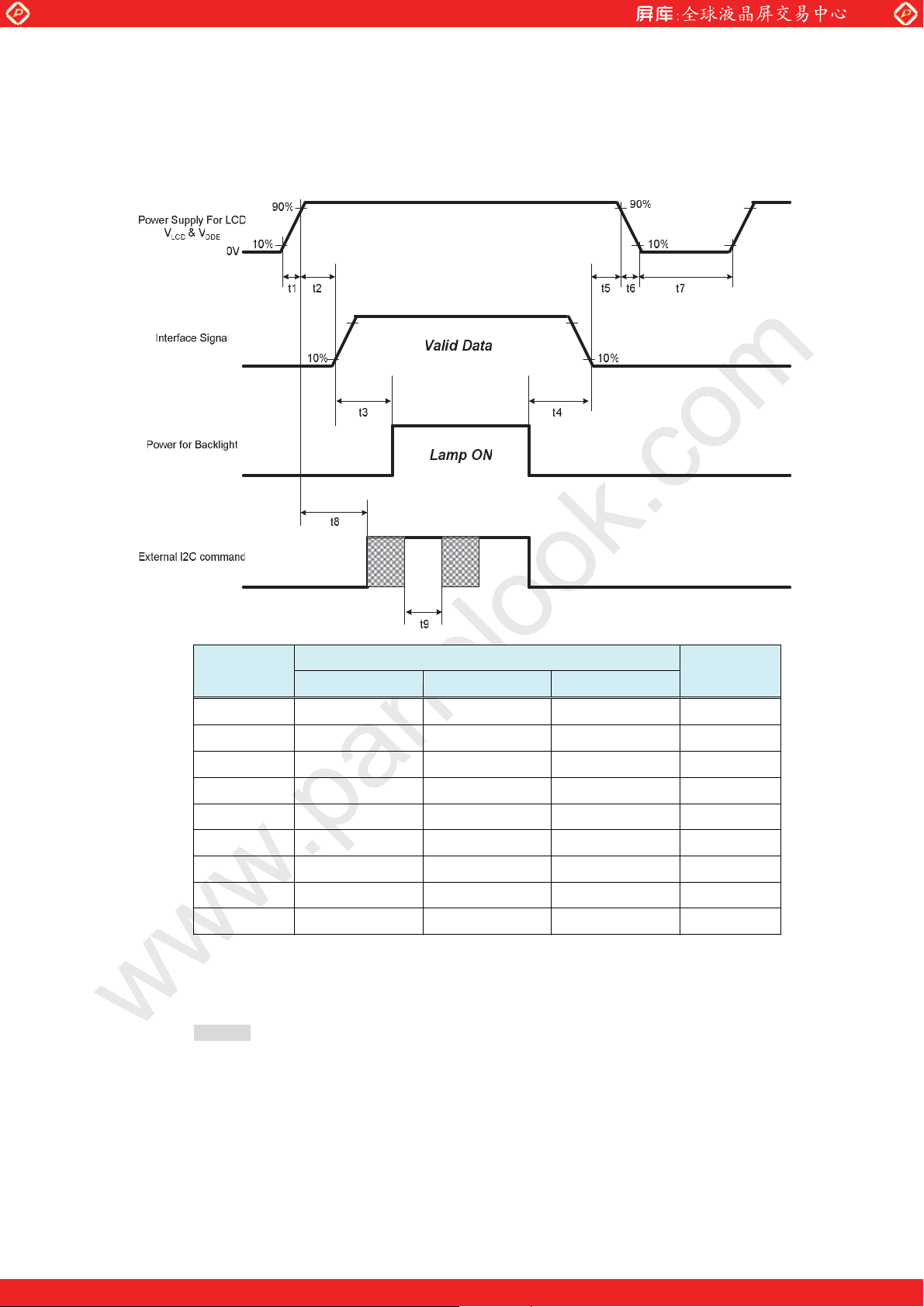
3.6 Power Sequence
www.panelook.com
Parameter
Min. Typ. Max.
t1 0.4 -- 30 ms
t2 2480 -- 2980 ms
t3 1300 -- -- ms
t4 10 -- -- ms
t5 0.1 -- 50 ms
t6 -- -- 300 ms
t7 500 -- -- ms
t8 2500 -- -- ms
t9 100 -- -- ms
Apply the lamp voltage within the LCD operating range. When the backlight turns on before the
LCD operation or the LCD turns off before the backlight turns off, the display may momentarily
become abnormal.
Caution: The above on/off sequence should be applied to avoid abnormal function in the display.
In case of handling, make sure to turn off the power when you plug the cable into the input
connector or pull the cable out of the connector.
Values
Unit
©Copyrig ht AU Optronics Corp.
2009 All Rights Reserved. T420HW04 V6 16/31
No Reproduction and Redistribution Allowed
One step solution for LCD / PDP / OLED panel application: Datasheet, inventory and accessory!
www.panelook.com
Page 18
Global LCD Panel Exchange Center
Backlight Power Specification
1. Electrical specification
No ITEM SYMBOL CONDITION MIN TYP MAX UNIT Note
www.panelook.com
1 Input Voltage V
2 Input C urrent I
3 Input Power P
4 Input inrush current I
DDB
DDB
DDB
RUSH
5 Output Frequency FBL V
ON/OFF Control
6
Voltage
V
BLON
ON V
OFF V
--- 21.6 24.0 26.4 V
V
=24V
DDB
6.94 7.3 7.66 A
100% Brightness
V
=24V
DDB
100% Brightness
V
=24V
DDB
100% Brightness
=24V 44 kHz
DDB
=24V 2.0 --- 5.0 V
DDB
=24V 0.0 --- 0.8 V
DDB
175 W
--- 9.9 A
DC
DC
DC
DC
DC
ON/OFF Control
7
Current
I
V
BLON
=24V 0 --- 2 mA
DDB
DC
Internal PWM
8
Control Voltage
IV
V
PWM
=24V 0 --- 3.3 V
DDB
DC
Ta =2 55, Turn on for 45minutes
* Note : At < 20% dimming ratio, AUO would not guarantee display performance & start at High
and Low Temperature condition.
©Copyrig ht AU Optronics Corp.
2009 All Rights Reserved. T420HW04 V6 17/31
No Reproduction and Redistribution Allowed
One step solution for LCD / PDP / OLED panel application: Datasheet, inventory and accessory!
www.panelook.com
Page 19
Global LCD Panel Exchange Center
2. Input specification
Connector 1: S14B-PH-SM3-TB(JST) or equivalent
Symbol Description
1 VDDB (Main Power) DV input 24.0 VDC
2 VDDB (Main Power) DV input 24.0 VDC
3 VDDB (Main Power) DV input 24.0 VDC
4 VDDB (Main Power) DV input 24.0 VDC
5 VDDB (Main Power) DV input 24.0 VDC
6 GND Ground
7 GND Ground
www.panelook.com
8 GND Ground
9 GND Ground
10 GND Ground
11 Reserved Please leave it open
BL On/Off control signal
12 VBLON (Enable Pin)
13
VDIM
14 NC
High/Open: On, Low: Off
(Low=0~ 0.8V, High=2.0~3.3V)
Internal PWM (3.3V,100% duty)/open for 100% luminance,
0V : 10% duty
©Copyrig ht AU Optronics Corp.
2009 All Rights Reserved. T420HW04 V6 18/31
No Reproduction and Redistribution Allowed
One step solution for LCD / PDP / OLED panel application: Datasheet, inventory and accessory!
www.panelook.com
Page 20

Global LCD Panel Exchange Center
4.Optical Specification
Optical characteristics are determined after the unit has been ‘ON’ and stable for approximately 60
minutes in a dark environment at 25. The values specified are at an approximate distance 50cm
from the LCD surface at a viewing angle of and equal to 0.
www.panelook.com
SR3 or equivalent
Fig.4-1 Optical measurement equipment and method
Parameter
Symbol
Values
Min. Typ. Max.
Units Notes
Contrast Ratio CR 4000 5000 1
Surface Luminance, white LWH 400 500
Luminance Variation
Response Time (Average)
WHITE
5p 1.3 3
T
5.5 ms 4,5 (Gray to Gray)
cd/
2
Color Coordinates
RED R
X
0.640
RY0.330
GREEN G
X
0.290
GY0.600
BLUE B
Typ.-0.03
X
0.150
Typ.+0.03
BY0.060
WHITE W
W
X
Y
0.280
0.290
Viewing Angle Contrast Ratio>10
x axis, right(=0)
x axis, left(=180)
y axis, up(=90)
y axis, down (=0)
r
l
u
d
89 Degree 6
89
89
89
©Copyrig ht AU Optronics Corp.
2009 All Rights Reserved. T420HW04 V6 19/31
No Reproduction and Redistribution Allowed
One step solution for LCD / PDP / OLED panel application: Datasheet, inventory and accessory!
www.panelook.com
Page 21

Global LCD Panel Exchange Center
Note:
1. Contrast Ratio (CR) is defined mathematically as:
www.panelook.com
Contrast ratio(CR)=
Brightness on the "white" state
Brightness on the "black" state
2. Surface luminance is luminance value at point 1 across the LCD surface 50cm from the surface with
all pixels displaying white. From more information see Fig. 4-2. When V
L
WH=Lon1
, Where L
is the luminance with all pixels displaying white at center 1 location.
on1
3V/4
V/2
V/4
DDB = 24V, IDDB = 6.4A.
H
1
H/2H/4
3H/4
Fig.4-2 Optical measurement point
3. The variation in surface luminance,
WHITE(5P)
=Maximum(L
is defined under 100% brightness as:
WHITE
, L
on1
on2
,…,L
)/Minimum(L
on5
on1
, L
on2
,…L
on5
)
V
©Copyrig ht AU Optronics Corp.
2009 All Rights Reserved. T420HW04 V6 20/31
No Reproduction and Redistribution Allowed
One step solution for LCD / PDP / OLED panel application: Datasheet, inventory and accessory!
www.panelook.com
Page 22

Global LCD Panel Exchange Center
4. Response Time:
(a) Tr = full black to full white, 10%~90%
(b) Tf = full white to full black, 90%~10%
(c) G-to-G: average response time among brightness of 0%, 25%, 50%, 75% &100%.
0% 25% 50% 75% 100%
0% tr: 0% 25% tr: 0% 50% tr: 0% 75% tr: 0% 100%
25% tf: 25% 0% tr: 25% 50% tr: 25% 75% tr: 25% 100%
50% tf: 50% 0% tf: 50% 25% tr: 50% 75% tr: 50% 100%
www.panelook.com
75% tf: 75% 0% tf: 75% 25% tf: 75% 50% tr: 75% 100%
100% tf: 100% 0% tf: 100% 25% tf: 100% 50% tf: 100% 75%
5. Viewing angle is the angle at which the contrast ratio is greater than 10. The angles are determined
for the horizontal or x axis and the vertical or y axis with respect to the z axis which is normal to the
LCD surface. For more information see Fig. 4-3. (Optical measurement by SR3)
Fig.4-3 Viewing Angle Definition
©Copyrig ht AU Optronics Corp.
2009 All Rights Reserved. T420HW04 V6 21/31
No Reproduction and Redistribution Allowed
One step solution for LCD / PDP / OLED panel application: Datasheet, inventory and accessory!
www.panelook.com
Page 23

Global LCD Panel Exchange Center
5.Mechanical Characteristics
The contents provide general mechanical characteristics for the model T420HW04. In addition the
figures in the next page are detailed mechanical drawing of the LCD.
Outline Dimension
Active Display Area
Weight 12600g (typ.)
Surface Treatment AG, 3H
www.panelook.com
Horizontal (typ.) 983.0mm
Vertical (typ.) 576.0mm
Depth (typ.) 52.5mm
Horizontal (typ.) 939.0mmBezel Area
Vertical (typ.) 531.26mm
Horizontal 930.24mm
Vertical 523.26mm
©Copyrig ht AU Optronics Corp.
2009 All Rights Reserved. T420HW04 V6 22/31
No Reproduction and Redistribution Allowed
One step solution for LCD / PDP / OLED panel application: Datasheet, inventory and accessory!
www.panelook.com
Page 24

Global LCD Panel Exchange Center
2D drawing
www.panelook.com
©Copyrig ht AU Optronics Corp.
2009 All Rights Reserved. T420HW04 V6 23/31
No Reproduction and Redistribution Allowed
One step solution for LCD / PDP / OLED panel application: Datasheet, inventory and accessory!
www.panelook.com
Page 25

Global LCD Panel Exchange Center
www.panelook.com
©Copyrig ht AU Optronics Corp.
2009 All Rights Reserved. T420HW04 V6 24/31
No Reproduction and Redistribution Allowed
One step solution for LCD / PDP / OLED panel application: Datasheet, inventory and accessory!
www.panelook.com
Page 26
Global LCD Panel Exchange Center
6.Reliability
Panel condition in RA test
Brightness: 500nits
No Test Item Condition
1 High temperature storage test Ta=60 300h
2 Low temperature storage test Ta= -20 300h
3 High temperature operation test Ta=50 300h
4 Low temperature operation test Ta=-5 300h
5 Vibration test
(non-operating)
6 Shock test
(non-operating)
7 Vibration test
(with carton)
8 Drop test
(with carton)
www.panelook.com
Wave form: random
Vibration level: 1.5G RMS
Bandwidth: 10-300Hz,
Duration: X, Y, Z 30min
One time each direction
Shock level: 50G
Waveform: half since wave, 11ms
Direction: ±X, ±Y, ±Z
One time each direction
Wave form: random
Vibration level: 1.5G RMS
Bandwidth: 10-200Hz,
Duration: X, Y, Z 30min
One time each direction
Height: 25.4cm
1 corner, 3 edges, 6 surfaces
(ASTMD4169-I)
Result Evaluation Criteria
There should be no change which might affect the practical display function when the display quality test is
conducted under normal operating condition.
©Copyrig ht AU Optronics Corp.
2009 All Rights Reserved. T420HW04 V6 25/31
No Reproduction and Redistribution Allowed
One step solution for LCD / PDP / OLED panel application: Datasheet, inventory and accessory!
www.panelook.com
Page 27

Global LCD Panel Exchange Center
7. International Standard
7-1. Safety
(1) UL60065, Underwriters Laboratories, Inc. (AUO file number : E204356)
Standard for Safety of Information Technology Equipment Including electrical Business
Equipment.
(2) CSA E60065, Canadian Standards Association
Standard for Safety of Information Technology Equipment Including Electrical Business
Equipment.
(3) IEC 60065 ver. 7
EUROPEAN STANDARD for Safety of Information Technology Equipment Including Electrical
Business Equipment.
www.panelook.com
th
,European Committee for Electro technical Standardization (CENELEC)
7-2. EMC
(1) ANSI C63.4 “Methods of Measurement of Radio-Noise Emissions from Low-Voltage Electrical and
Electrical Equipment in the Range of 9kHz to 40GHz. “American National standards
Institute(ANSI), 1992
(2) C.I.S.P.R “Limits and Methods of Measurement of Radio Interface Characteristics of Information
Technology Equipment. ” International Special committee on Radio Interference.
(3) EN 55022 “Limits and Methods of Measurement of Radio Interface Characteristics of Information
Technology Equipment. ” European Committee for Electro technical Standardization. (CENELEC),
1998
©Copyrig ht AU Optronics Corp.
2009 All Rights Reserved. T420HW04 V6 26/31
No Reproduction and Redistribution Allowed
One step solution for LCD / PDP / OLED panel application: Datasheet, inventory and accessory!
www.panelook.com
Page 28

Global LCD Panel Exchange Center
g
p
p
t
8.Packing
8-1 Packing Instruction
1pcs Module/E S D B a
www.panelook.com
Module
Cushion to
Cushion se
Cus hion down
H Tape
7
cs /1 carton
Package information:
Carton outside dimension : 1060x560x678mm , Carton/Package weight :6 kg
©Copyright AU Optronics Corp.
2009 All Rights Reserved. T420HW04 V1
No Reproduction and Redistribution Allowed
27/31
One step solution for LCD / PDP / OLED panel application: Datasheet, inventory and accessory!
www.panelook.com
Page 29

Global LCD Panel Exchange Center
Shipping label
Sample Stage (without green & safety mark):
Mass Production Stage (with green & safety mark) :
www.panelook.com
Green Mark Description:
For Pb Free products, AUO will add
For RoHS compatible products, AUO will add
Note: The Green Mark will be present only when the green documents have been ready by AUO Internal Green
Team. (The definition of green design follows the AUO green design checklist.)
for identification.
for identification.
Carton label
©Copyright AU Optronics Corp.
2009 All Rights Reserved. T420HW04 V1
No Reproduction and Redistribution Allowed
One step solution for LCD / PDP / OLED panel application: Datasheet, inventory and accessory!
28/31
www.panelook.com
Page 30

Global LCD Panel Exchange Center
Pallet information
By air cargo : : (2x1) x1 layers, one pallet put 2 boxes, 1layers(1pallet) total 14 pcs module.
By sea : (2x1) x3 layers, one pallet put 2 boxes, 3l ayers(3pallet) total 42 pcs module.
Pallet dimension : 1150x1070x132mm
Pallet weight : 10kg
By air total weight : 95kg/box X 2 boxes=190 kg (with 1 pallet weight 200kg)
By sea total weight : 95kg/box X 6 boxes=570 kg (with 3 pallet weight 600kg)
Stretch film
www.panelook.com
Moisture-proof filmCorner angle
Label
PET band
Corner angle
Pallet
©Copyright AU Optronics Corp.
2009 All Rights Reserved. T420HW04 V1
No Reproduction and Redistribution Allowed
One step solution for LCD / PDP / OLED panel application: Datasheet, inventory and accessory!
29/31
www.panelook.com
Page 31

Global LCD Panel Exchange Center
9.PRECAUTIONS
Please pay attention to the followings when you use this TFT LCD module.
9-1 MOUNTING PRECAUTIONS
(1) You must mount a module using holes arranged on back side of panel.
(2) Please attach the surface transparent protective plate to the surface in order to protect the polarizer.
Transparent protective plate should have sufficient strength in order to the resist external force.
(3) You should adopt radiation structure to satisfy the temperature specification.
(4) Acetic acid type and chlorine type materials for the cover case are not desirable because the former
generates corrosive gas of attacking the polarizer at high temperature and the latter causes circuit break
by electro-chemical reaction.
(5) Do not touch, push or rub the exposed polarizers with glass, tweezers or anything harder than HB pencil
lead. And please do not rub with dust clothes with chemical treatment. Do not touch the surface of
polarizer for bare hand or greasy cloth. (Some cosmetics are detrimental to the polarizer.)
(6) When the surface becomes dusty, please wipe gently with absorbent cotton or other soft materials like
chamois soaks with petroleum benzene. Normal-hexane is recommended for cleaning the adhesives
used to attach front/ rear polarizers. Do not use acetone, toluene and alcohol because they cause
chemical damage to the polarizer.
(7) Wipe off saliva or water drops as soon as possible. Their long time contact with polarizer causes
deformations and color fading.
(8) Do not open the case because inside circuits do not have sufficient strength.
www.panelook.com
9-2 OPERATING PRECAUTIONS
(1) The spike noise causes the mis-operation of circuits. It should be lower than following voltage: V=
200mV(Over and under shoot voltage)
(2) Response time depends on the temperature. (In lower temperature, it becomes longer..)
(3) Bri ghtness depends on the temperature. (In lower temperature, it becomes lower.) And in lower
temperature, response time (required time that brightness is stable after turned on) becomes longer.
(4) Be careful for condensation at sudden temperature change. Condensation makes damage to polarizer
or electrical contacted parts. And after fading condensation, smear or spot will occur.
(5) When fixed patterns are displayed for a long time, remnant image is likely to occur.
(6) Module has high frequency circuits. Sufficient suppression to the electromagnetic interference shall be
done by system manufacturers. Grounding and shielding methods may be important to minimize the
interface.
9-3 ELECTROSTATIC DISCHARGE CONTROL
Since a module is composed of electronic circuits, it is not strong to electrostatic discharge. Make certain
that treatment persons are connected to ground through wrist band etc. And don ’t touch interface pin
©Copyright AU Optronics Corp.
2009 All Rights Reserved. T420HW04 V1
No Reproduction and Redistribution Allowed
30/31
One step solution for LCD / PDP / OLED panel application: Datasheet, inventory and accessory!
www.panelook.com
Page 32

Global LCD Panel Exchange Center
directly.
9-4 PRECAUTIONS FOR STRONG LIGHT EXPOSURE
Strong light exposure causes degradation of polarizer and color filter.
9-5 STORAGE
When storing modules as spares for a long time, the following precautions are necessary.
(1) Store them in a dark place. Do not expose the module to sunlight or fluorescent light. Keep the
temperature between 5 and 35 at normal humidity.
(2) The polarizer surface should not come in contact with any other object. It is recommended that they be
stored in the container in which they were shipped.
www.panelook.com
9-6 HANDLING PRECAUTIONS FOR PROTECTION FILM
(1) The protection film is attached to the bezel with a small masking tape. When the protection film is peeled
off, static electricity is generated between the film and polarizer. This should be peeled off slowly and
carefully by people who are electrically grounded and with well ion-blown equipment or in such a
condition, etc.
(2) When the module with protection film attached is stored for a long time, sometimes there remains a very
small amount of flue still on the Bezel after the protection film is peeled off.
(3) You can remove the glue easily. When the glue remains on the Bezel or its vestige is recognized, please
wipe them off with absorbent cotton waste or other soft material like chamois soaked with
normal-hexane.
©Copyright AU Optronics Corp.
2009 All Rights Reserved. T420HW04 V1
No Reproduction and Redistribution Allowed
One step solution for LCD / PDP / OLED panel application: Datasheet, inventory and accessory!
31/31
www.panelook.com
 Loading...