

Page 1
Global LCD Panel Exchange Center
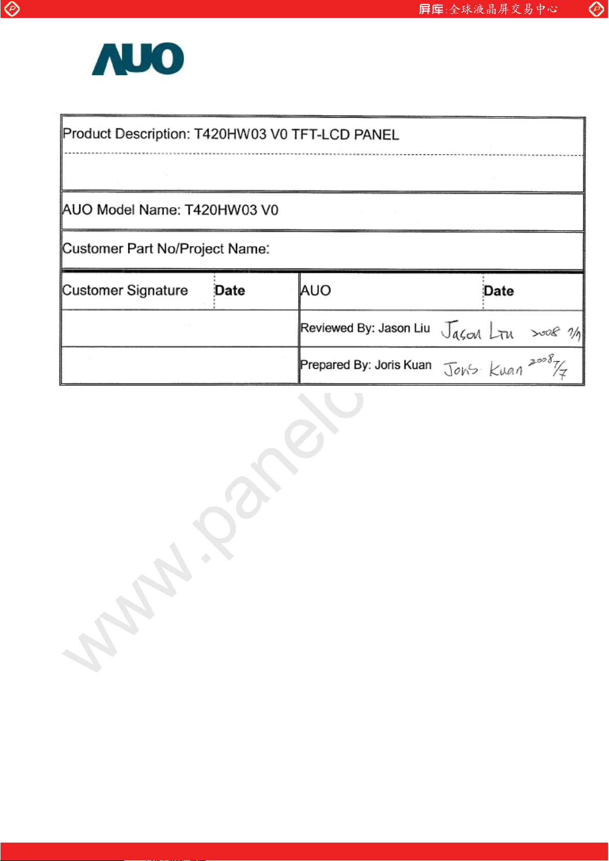
Product Description: T420HW03 V0 TFT-LCD PANEL
AUO Model Name: T420HW03 V0
Customer Part No/Project Name:
Customer Signature Date AUO Date
www.panelook.com
Reviewed By: Jason Liu
Prepared By: Joris Kuan
©Copyright AU Optronics, Inc.
January, 2008 All Rights Reserved. T420HW03 V0 0/29
No Reproduction and Redistribution Allowed
One step solution for LCD / PDP / OLED panel application: Datasheet, inventory and accessory!
www.speclcd.com
www.panelook.com
Page 2

Global LCD Panel Exchange Center
Document Version: 1.3
Date:2008/7/07
Product Functional Specification
42” Full-HD Color TFT-LCD Module
Model Name: T420HW03 V0
www.panelook.com
() Preliminary Specification
(*) Final Specification
Note : This specification is subject to change without notice.
©Copyright AU Optronics, Inc.
January, 2008 All Rights Reserved. T420HW03 V0 1/29
No Reproduction and Redistribution Allowed
One step solution for LCD / PDP / OLED panel application: Datasheet, inventory and accessory!
www.panelook.com
Page 3
Global LCD Panel Exchange Center
Contents
COVER
CONTENTS
GENERAL DESCRIPTION1
ABSOLUTE MAXIMUM RATINGS2
www.panelook.com
ITEMNo
RECORD OF REVISIONS
ELECTRICAL SPECIFICATIONS3
ELECTRICAL CHARACTREISTICS3-1
INTERFACE CONNECTIONS3-2
SIGNAL TIMING SPECIFICATIONS3-3
SIGNAL TIMING WAVEFORMS3-4
COLOR INPUT DATA REFERNECE3-5
POWER SEQUENCE3-6
OPTICAL SPECIFICATIONS4
MECHANICAL CHARACTERISTICS5
RELIABILITY6
7
INTERNATIONAL STANDARDS
SAFETY7-1
EMC7-2
8
PACKI NG
PRECAUTIONS9
©Copyright AU Optronics, Inc.
January, 2008 All Rights Reserved. T420HW03 V0 2/29
No Reproduction and Redistribution Allowed
One step solution for LCD / PDP / OLED panel application: Datasheet, inventory and accessory!
www.panelook.com
Page 4
Global LCD Panel Exchange Center
www.panelook.com
Record of Revision
Version Date No Old Description New Description Remark
1.0 2008/5/28 First release
3-3 Update LVDS timing1.1 2008/6/10
5 Update 2D drawing
1.2 2008/7/2
1.3 2008/7/7 5 Update 2D drawing
1
EPWM 120~240Hz
3-3 Update LVDS timing
4
Add turn on IDDB
EPWM 95~240Hz
Add gamma = 2.3
©Copyright AU Optronics, Inc.
January, 2008 All Rights Reserved. T420HW03 V0 3/29
No Reproduction and Redistribution Allowed
One step solution for LCD / PDP / OLED panel application: Datasheet, inventory and accessory!
www.panelook.com
Page 5
Global LCD Panel Exchange Center
1. General Description
This specification applies to the 42 inch Color TFT-LCD Module T420HW03 V0. This LCD module has
a TFT active matrix type liquid crystal panel 1920x1080 pixels, and diagonal size of 42 inch. This
module supports 1920x1080 Full-HD mode (Non-interlace).
Each pixel is divided into Red, Green and Blue sub-pixels or dots which are arranged in vertical stripes.
Gray scale or the brightness of the sub-pixel color is determined with a 10-bit gray scale signal for
each dot.
The T420HW03 V0 has been designed to apply the 10-bit 4 channel LVDS interface method. It is
intended to support displays where high brightness, wide viewing angle, high color saturation, and
high color depth are very important.
www.panelook.com
* General Information
Items Specification Unit Note
Active Screen Size 42.02 inches
Display Area 930.24(H) x 523.26(V) mm
Outline Dimension 967.0(H) x 559.0(V) x 41.1(D) mm With inverter
Driver Element a-Si TFT active matrix
Display Colors 1073M Colors
Number of Pixels 1920 x 1080 Pixel
Pixel Pitch 0.4845 mm
Pixel Arrangement RGB vertical stripe
Display Mode Normally Black
Lamp quantity, type 24pcs, Straight type pcs
Surface Treatment Anti-Glare coating (Haze 11%)
Hard coating (3H)
©Copyright AU Optronics, Inc.
January, 2008 All Rights Reserved. T420HW03 V0 4/29
No Reproduction and Redistribution Allowed
One step solution for LCD / PDP / OLED panel application: Datasheet, inventory and accessory!
www.panelook.com
Page 6
Global LCD Panel Exchange Center
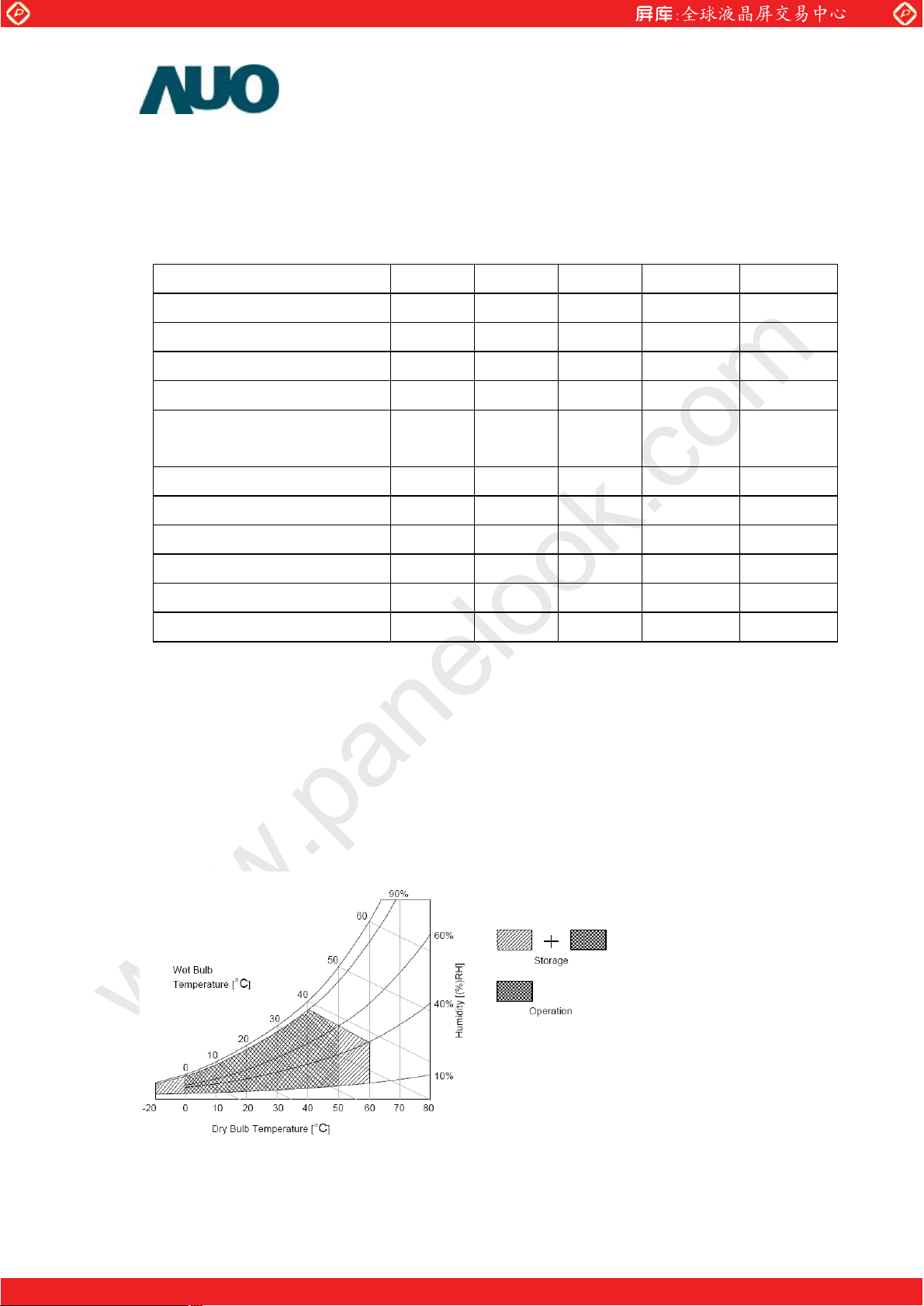
Absolute Maximum Ratings
The following are maximum values which, if exceeded, may cause faulty operation or damage to the
unit.
Item Symbol Min Max Unit Note
Power Supply Input Voltage VDD -0.3 14 [Volt] 1
Logic Input Voltage Vin -0.3 4 [Volt] 1
BLU Input Voltage VDDB -0.3 26.4 [Volt] 1
BLU Brightness Control Voltage BLON -0.3 3.6 [Volt] 1
www.panelook.com
Ambient Operating
Temperature
Ambient Operating Humidity HOP 10 80 [%RH] 2
Storage Temperature TST -20 +60 [oC] 2
Storage Humidity HST 10 80 [%RH] 2
Shock (non-operation) - 50 G 3
Vibration (non-operation) - 1.5 G 4
Thermal shock -20 60 C 5
Note 1 : Duration = 50msec
Note 2 : Maximum Wet-Bulb should be 50 and No condensation.
Note 3 : Half sine wave, shock level : 50G(11ms), direction : ±x, ±y, ±z (one time each direction)
Note 4 : Wave form : Random, vibration level : 1.5G RMS, Bandwidth : 10~500Hz
Duration : X,Y,Z 30min (one time each direction)
Note 5 : -20C/1hr ~ 60C/1hr, 100 cycles
TOP 0 +50 [oC] 2
©Copyright AU Optronics, Inc.
January, 2008 All Rights Reserved. T420HW03 V0 5/29
No Reproduction and Redistribution Allowed
One step solution for LCD / PDP / OLED panel application: Datasheet, inventory and accessory!
www.panelook.com
Page 7
Global LCD Panel Exchange Center
V
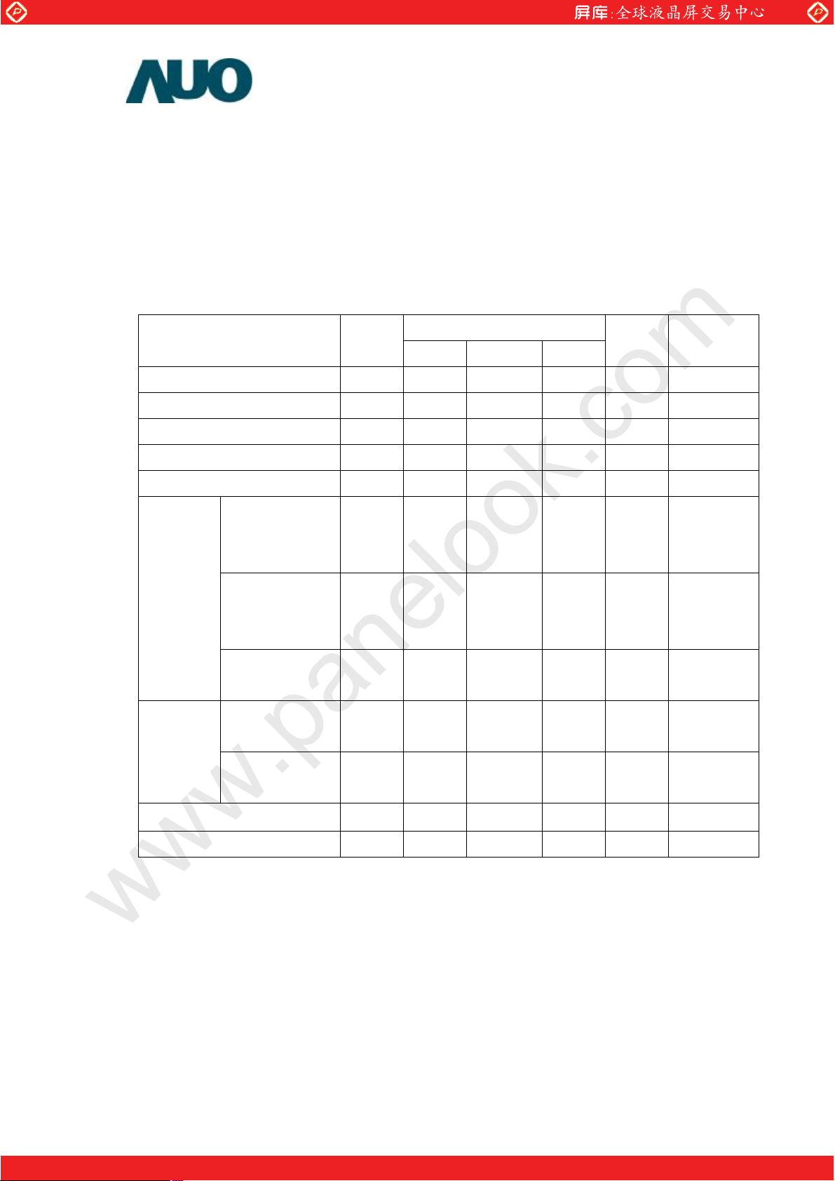
2. Electrical Specification
The T420HW03 requires two power inputs. One is employed to power the LCD electronics and to drive
the TFT array and liquid crystal. The second input, which powers the CCFL, is typically generated by
an inverter.
3-1 Electrical Characteristics
www.panelook.com
ValuesParameter Symbol
Min Typ Max
LCD:
Power Supply Input Voltage Vdd 10.8 12 13.2 Vdc
Power Supply Input Current Idd - 1 1.7 A 1
Power Consumption Pc - 12 20.4 Watt 1
Inrush Current I
LVDS
Interface
CMOS
Differential Input
High Threshold
oltage
Differential Input
Low Threshold
Voltage
Common Input
Voltage
Input High
RUSH
TH +100 mV
V
VTL -100 mV
V
CIM 0.6 1.2 1.8 V
VIH
-- 4A5
2.0 3.3 Vdc
Unit Notes
4
4
Interface
Backlight Power Consumption
Life Time 50000 60000 Hours 3
Do not attach a conducting tape to lamp connecting wire. If the lamp wire attach to conducting
tape, TFT-LCD Module have a low luminance and the inverter has abnormal action because
leakage current occurs between lamp wire and conducting tape.
The relative humidity must not exceed 80% non-condensing at temperatures of 40 or less. At
temperatures greater than 40, the wet bulb temperature must not exceed 39. When operate
at low temperatures, the brightness of CCFL will drop and the lifetime of CCFL will be reduced.
©Copyright AU Optronics, Inc.
January, 2008 All Rights Reserved. T420HW03 V0 6/29
No Reproduction and Redistribution Allowed
Threshold Voltage
Input Low
Threshold Voltage
(High)
V
IL
(Low)
0 0.8 Vdc
- 156 165 Watt 2
One step solution for LCD / PDP / OLED panel application: Datasheet, inventory and accessory!
www.panelook.com
Page 8
Global LCD Panel Exchange Center
s
s
Note :
1. Vdd=12.0V, fv=120Hz, f
pattern
2. The Backlight power consumption shown above does include loss of external inverter at 25.
The used lamp current is the lamp typical current
3. The life is determined as the time at which luminance of the lamp is 50% compared to that of
initial value at the typical lamp current on condition of continuous operating at 252.
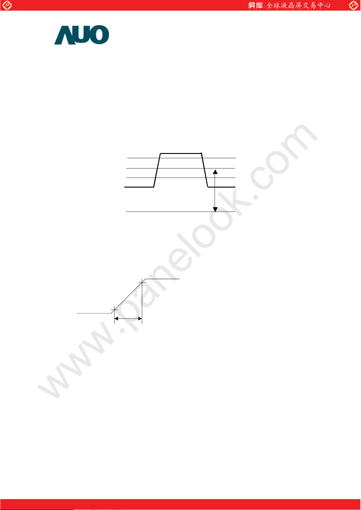
4. VCIM = 1.2V
VTH
VCIM
VTL
www.panelook.com
CLK=80 Mhz , 25, Vdd Duration time= 470
µ
, Test pattern : white
0V
Figure : LVDS Differential Voltage
5. Measurement Condition: Rising time = 470s
0.9 Vdd
GND
0.1 Vdd
470
µ
Vdd
©Copyright AU Optronics, Inc.
January, 2008 All Rights Reserved. T420HW03 V0 7/29
No Reproduction and Redistribution Allowed
One step solution for LCD / PDP / OLED panel application: Datasheet, inventory and accessory!
www.panelook.com
Page 9
Global LCD Panel Exchange Center
3-2 Interface Connections
- LCD connector: FI-RE51S-HF (JAE) or equivalent
www.panelook.com
No
1
2
3
4
5
6
7
8
9
10
11
12
13
14
Symbol
NC
NC
NC
NC
NC
NC
LVDS SEL
NC
NC
NC
GND
R1_0-
R1_0+
R1_1-
Description No
No connection 27
No connection 28
No connection 29
No connection 30
No connection 31
No connection 32
LVDS order, Low /Open for NS
33
,High for JEIDA
No connection 34
No connection 35
No connection 36
Ground 37
LVDS Channel 1, Signal 0- 38
LVDS Channel 1, Signal 0+ 39
LVDS Channel 1, Signal 1- 40
Symbol
NC or GND
R2_0-
R2_0+
R2_1-
R2_1+
R2_2-
R2_2+
GND
R2_CLK-
R2_CLK+
GND
R2_3-
R2_3+
R2_4-
Description
No Connect or Ground
LVDS Channel 2, Signal 0-
LVDS Channel 2, Signal 0+
LVDS Channel 2, Signal 1-
LVDS Channel 2, Signal 1+
LVDS Channel 2, Signal 2-
LVDS Channel 2, Signal 2+
Ground
LVDS Channel 2, Clock -
LVDS Channel 2, Clock +
Ground
LVDS Channel 2, Signal 3-
LVDS Channel 2, Signal 3+
LVDS Channel 2, Signal 4-
15
16
17
18
19
20
21
22
23
24
25
26
R1_1+
R1_2-
R1_2+
GND
R1_CLK-
R1_CLK+
GND
R1_3-
R1_3+
R1_4-
R1_4+
NC or GND
LVDS Channel 1, Signal 1+ 41
LVDS Channel 1, Signal 2- 42
LVDS Channel 1, Signal 2+ 43
Ground 44
LVDS Channel 1, Clock - 45
LVDS Channel 1, Clock + 46
Ground 47
LVDS Channel 1, Signal 3- 48
LVDS Channel 1, Signal 3+ 49
LVDS Channel 1, Signal 4- 50
LVDS Channel 1, Signal 4+ 51
No Connect or Ground -
R2_4+
NC or GND
NC or GND
GND
GND
GND
V
LCD
V
LCD
V
LCD
V
LCD
V
LCD
-
LVDS Channel 2, Signal 4+
No Connect or Ground
No Connect or Ground
Ground
Ground
Ground
Operating Voltage supply, +12V DC regulated
Operating Voltage supply,+12V DC regulated
Operating Voltage supply, +12V DC regulated
Operating Voltage supply, +12V DC regulated
Operating Voltage supply, +12V DC regulated
-
©Copyright AU Optronics, Inc.
January, 2008 All Rights Reserved. T420HW03 V0 8/29
No Reproduction and Redistribution Allowed
One step solution for LCD / PDP / OLED panel application: Datasheet, inventory and accessory!
www.panelook.com
Page 10
Global LCD Panel Exchange Center
- LCD connector 2 : FI-RE41S-HF (JAE) or equivalent
www.panelook.com
No
1
2
3
4
5
6
7
8
9
10
11
12
13
14
15
Symbol
NC
NC
NC
NC
NC
NC
NC
NC
GND
R3_0-
R3_0+
R3_1-
R3_1+
R3_2-
R3_2+
Description No
No connection 27
No connection 28
No connection 29
No connection 30
No connection 31
No connection 32
No connection 33
No connection 34
Ground 35
LVDS Channel 3, Signal 0- 36
LVDS Channel 3, Signal 0+ 37
LVDS Channel 3, Signal 1- 38
LVDS Channel 3, Signal 1+ 39
LVDS Channel 3, Signal 2- 40
LVDS Channel 3, Signal 2+ 41
Symbol
R4_0+
R4_1-
R4_1+
R4_2-
R4_2+
GND
R4_CLK-
R4_CLK+
GND
R4_3-
R4_3+
R4_4-
R4_4+
NC or GND
NC or GND
Description
LVDS Channel 4, Signal 0+
LVDS Channel 4, Signal 1-
LVDS Channel 4, Signal 1+
LVDS Channel 4, Signal 2-
LVDS Channel 4, Signal 2+
Ground
LVDS Channel 4, Clock -
LVDS Channel 4, Clock +
Ground
LVDS Channel 4, Signal 3-
LVDS Channel 4, Signal 3+
LVDS Channel 4, Signal 4-
LVDS Channel 4, Signal 4+
No Connect or Ground
No Connect or Ground
GND
16
17
18
19
20
21
22
23
24
25
26
R3_CLK-
R3_CLK+
GND
R3_3-
R3_3+
R3_4-
R3_4+
NC or GND
NC or GND
R4_0-
Ground
LVDS Channel 3, Clock -
LVDS Channel 3, Clock +
Ground
LVDS Channel 3, Signal 3-
LVDS Channel 3, Signal 3+
LVDS Channel 3, Signal 4-
LVDS Channel 3, Signal 4+
No Connect or Ground
No Connect or Ground
LVDS Channel 4, Signal 0-
Note: 1. All GND (ground) pin should be connected together to the LCD module’s metal frame.
2. All V
( power input ) pins should be connected.
LCD
©Copyright AU Optronics, Inc.
January, 2008 All Rights Reserved. T420HW03 V0 9/29
No Reproduction and Redistribution Allowed
One step solution for LCD / PDP / OLED panel application: Datasheet, inventory and accessory!
www.panelook.com
Page 11

Global LCD Panel Exchange Center
LVDS Option = HighJEIDA
4 CH LVDS data mapping
www.panelook.com
LVDS Option = Low/OpenNS
©Copyright AU Optronics, Inc.
January, 2008 All Rights Reserved. T420HW03 V0 10/29
No Reproduction and Redistribution Allowed
One step solution for LCD / PDP / OLED panel application: Datasheet, inventory and accessory!
www.panelook.com
Page 12

Global LCD Panel Exchange Center
Backlight Connector Pin Configuration
1. Electrical specification
No ITEM SYMBOL CONDITION MIN TYP MAX UNIT Note
www.panelook.com
1 Input Voltage V
I
DDB
DDB
--- 21.6 24.0 26.4 V
V
=24V
DDB
100% Brightness
( Turn On Condition )
2 Input Current
V
=24V
DDB
I
DDB
100% Brightness
(Stable Condition )
V
=24V
3 Input Power P
DDB
DDB
100% Brightness
V
=24V
4 Input inrush current I
RUSH
DDB
100% Brightness
5 Output Frequency FBL V
ON/OFF Control
6
Voltage
V
BLON
ON V
OFF V
=24V --- 42 --- kHz
DDB
=24V 2.0 --- 3.3 V
DDB
=24V 0.0 --- 0.8 V
DDB
ON/OFF Control
7
I
V
BLON
=24V 0 --- 2 mADC
DDB
Current
- - 7.2 A
6.1 6.5 6.9 A
--- 156 165 W
--- --- 10 A
DC
DC
DC
DC
DC
DC
External PWM
8
Control Voltage
External PWM
9
Control Current
EV
EI
PWM
PW M
MAX --- 2.0 --- 3.3 V
MIN --- 0 --- 0.8 V
DC
DC
MAX PWM=100% 0 --- 2 mADC
MIN PW M=30% 0 --- 2 mADC
External PWM Duty
10
ED
PWM
--- 20 --- 100 %
Ratio
External PWM
11
EF
PWM
--- 95 --- 240 Hz
Frequency
Internal PWM
12
IV
V
PW M
=24V 0 --- 3.3 V
DDB
DC
Control Voltage
Ta =2 55, Turn on for 45minutes
10% dimming stable brightness function is ok but not guarantee uniformity and flicker.
©Copyright AU Optronics, Inc.
January, 2008 All Rights Reserved. T420HW03 V0 11/29
No Reproduction and Redistribution Allowed
One step solution for LCD / PDP / OLED panel application: Datasheet, inventory and accessory!
www.panelook.com
Page 13

Global LCD Panel Exchange Center
2. Input specification
Connector 1: S14B-PH-SM3-TB(JST) or equivalent
Pin No Symbol Description
1 VDDB Operating Voltage Supply, +24V DC regulated
2 VDDB Operating Voltage Supply, +24V DC regulated
3 VDDB Operating Voltage Supply, +24V DC regulated
4 VDDB Operating Voltage Supply, +24V DC regulated
5 VDDB Operating Voltage Supply, +24V DC regulated
6BLGND Ground and Current Return
7BLGND Ground and Current Return
8BLGND Ground and Current Return
9BLGND Ground and Current Return
10 BLGND Ground and Current Return
www.panelook.com
11 Det Output of Detect error: Low=NG , Open/High=OK
12 VBLON BL On-Off: Open/High (3.3V) for BL On as default
External PWM (AC Signal Control Duty);
13
P
Internal PWM (DC Power Control Duty, 0~3.3V);
(2)
DIM
Open/High (+3.3V, 100% Duty) for 100%
14
DIM
P
Selection
(3,4)
GND: External PWM dimming;
Open/High (3.3V): Internal PWM dimming.
Note (1)Det is Output pin for detect power error.
Note (2)PDIM is PWM duty control input for +3.3V TTL level signal or DC voltage by Pin 14 input. This
input signal is (a) continuous pulse signal with +3.3V, TTL level signal spec, or (b) DC power
with 0~3.3V. If this is Open or +3.3V, 100% duty (i.e. +3.3V, DC level), backlight should
perform 100% luminance. Duty ratio of this input signal should be proportional relationship in
certain range of control without any kind of inherent side effect like waterfall effect on screen.
Guaranteed duty range and dimming ratio should be specified with supplementary
measurement result.
Note (3) Pin 14 is the selection pin for PWM control method; if this pin is connected to GND, PDIM
input of Pin 13 should have logic level duty signal for PWM control. If this is set to High or
Open, Pin 13 should have DC level signal therefore the Inverter should have Saw Tooth Wave
Generator to generate internal PWM signal. Default setting is“Not Connected”, Pin13ofPWM
control should have DC Level signal for PWM.
Note (4) Pin 14 selection vs. Pin 11/13 control function table:
Pin 13
Default: Open/High: 100%
Pin 14 =GND
Pin 14 =Open/High
External PWM
(AC Signal Control Duty)
Internal PWM
(DC Power Control Duty)
©Copyright AU Optronics, Inc.
January, 2008 All Rights Reserved. T420HW03 V0 12/29
No Reproduction and Redistribution Allowed
One step solution for LCD / PDP / OLED panel application: Datasheet, inventory and accessory!
www.panelook.com
Page 14

Global LCD Panel Exchange Center
Slave Board:
Connector 2: S12B-PH-SM3-TB(JST) or equivalent
Pin No Symbol Description
1 VDDB Operating Voltage Supply, +24V DC regulated
2 VDDB Operating Voltage Supply, +24V DC regulated
3 VDDB Operating Voltage Supply, +24V DC regulated
4 VDDB Operating Voltage Supply, +24V DC regulated
5 VDDB Operating Voltage Supply, +24V DC regulated
6BLGND Ground and Current Return
7BLGND Ground and Current Return
8BLGND Ground and Current Return
9BLGND Ground and Current Return
www.panelook.com
10 BLGND Ground and Current Return
11 NC
12 NC
©Copyright AU Optronics, Inc.
January, 2008 All Rights Reserved. T420HW03 V0 13/29
No Reproduction and Redistribution Allowed
One step solution for LCD / PDP / OLED panel application: Datasheet, inventory and accessory!
www.panelook.com
Page 15

Global LCD Panel Exchange Center
3-3 Signal Timing Specifications
This is the signal timing required at the input of the User connector. All of the interface signal timing
should be satisfied with the following specifications for it’s proper operation.
Timing Table (DE only Mode)
Vertical Frequency Range (120Hz)
Signal Item Symbol Min Type Max Unit
www.panelook.com
Period Tv 1096 1130 1160 Th
Active Tdisp (v) 1080 Th
Vertical Section
Horizontal Section
Clock Frequency Freq 69.4425 75.936 80.74 MHz
Vertical Frequency Frequency Vs -- 120 -- Hz
Horizontal Frequency Frequency Hs 131.52 135.6 139.2 KHz
Vertical Frequency Range (100Hz)
Signal Item Symbol Min Type Max Unit
Vertical Section
Blanking Tblk (v) 16 50 80 Th
Period Th 528 560 580 Tclk
Active Tdisp (h) 480 Tclk
Blanking Tblk (h) 48 80 100 Tclk
Period Tv 1200 1280 1392 Th
Active Tdisp (v) 1080 Th
Blanking Tblk (v) 120 200 312 Th
Period Th 550 560 580 Tclk
Active Tdisp (h) 480 Tclk
Horizontal Section
Clock Frequency Freq 66 71.68 80.736 MHz
Vertical Frequency Frequency Vs -- 100 -- Hz
Horizontal Frequency Frequency Hs 120 128 139.2 KHz
©Copyright AU Optronics, Inc.
January, 2008 All Rights Reserved. T420HW03 V0 14/29
No Reproduction and Redistribution Allowed
Blanking Tblk (h) 70 80 100 Tclk
One step solution for LCD / PDP / OLED panel application: Datasheet, inventory and accessory!
www.panelook.com
Page 16

Global LCD Panel Exchange Center
3-4 Signal Timing Waveforms
www.panelook.com
(even)
M-6
M-4
M-2
M
2
4
6
RGB Data
Pixel
Pixel
Pixel
Pixel
Invalid Data
Pixel
Pixel
Pixel
(odd)
M-7
M-5
M-3
M-1
1
3
5
RGB Data
Tclk
CLK
RGB
Data
Line
N
Invalid Data Invalid Data
Line
1
Line
2
DE
Th
Tv
DE
Pixel
Pixel
Pixel
Pixel
Invalid Data
Pixel
Pixel
Pixel
8
10
12
M-4
M-2
M
2
4
Pixel
Pixel
Pixel
Pixel
Pixel
Pixel
Invalid Data
Pixel
Pixel
7
9
11
M-5
M-3
M-1
1
3
Pixel
Pixel
Pixel
Pixel
Pixel
Pixel
Invalid Data
Pixel
Pixel
Tdisp (h) Tblk( h)
Th
Line
3
Tdisp(v)Tblk (v)
Line
4
Line
N
©Copyright AU Optronics, Inc.
January, 2008 All Rights Reserved. T420HW03 V0 15/29
No Reproduction and Redistribution Allowed
One step solution for LCD / PDP / OLED panel application: Datasheet, inventory and accessory!
www.panelook.com
Page 17

Global LCD Panel Exchange Center
3-5 Color Input Data Reference
The brightness of each primary color (red, green and blue) is based on the 10 bit gray scale data input
for the color; the higher the binary input, the brighter the color. The table below provides a reference for
color versus data input.
COLOR DATA REFERENCE
www.panelook.com
©Copyright AU Optronics, Inc.
January, 2008 All Rights Reserved. T420HW03 V0 16/29
No Reproduction and Redistribution Allowed
One step solution for LCD / PDP / OLED panel application: Datasheet, inventory and accessory!
www.panelook.com
Page 18

Global LCD Panel Exchange Center
3-6 Power Sequence
1. Power sequence of panel
www.panelook.com
Values
Parameter
t1 0.47 - 30 ms
t2 0.1 - 50 ms
t3 500 - - ms
t4 100 - - ms
t5 0.1 - 50 ms
t6 - 30 ms
t7 1000 - - ms
Apply the lamp voltage within the LCD operating range. When the backlight turns on before the LCD
operation or the LCD turns off before the backlight turns off, the display may momentarily become
abnormal.
Caution : The above on/off sequence should be applied to avoid abnormal function in the display. In
case of handling, make sure to turn off the power when you plug the cable into the input connector or
pull the cable out of the connector.
Min. Typ. Max.
Units
©Copyright AU Optronics, Inc.
January, 2008 All Rights Reserved. T420HW03 V0 17/29
No Reproduction and Redistribution Allowed
One step solution for LCD / PDP / OLED panel application: Datasheet, inventory and accessory!
www.panelook.com
Page 19

Global LCD Panel Exchange Center
2. Power sequence of inverter
www.panelook.com
ValuesParameter
Min. Typ. Max.
T1 20 - - ms
T2 500 - - ms
T3 250 - - ms
T4 0 - - ms
T5 1 - - ms
T6 10 ms
©Copyright AU Optronics, Inc.
January, 2008 All Rights Reserved. T420HW03 V0 18/29
No Reproduction and Redistribution Allowed
Units
One step solution for LCD / PDP / OLED panel application: Datasheet, inventory and accessory!
www.panelook.com
Page 20

Global LCD Panel Exchange Center
4. Optical Specification
Optical characteristics are determined after the unit has been ‘ON’ and stable for approximately 60
minutes in a dark environment at 25. The values specified are at an approximate distance 50cm
from the LCD surface at a viewing angle of and equal to 0.
Fig.4-1 Optical measurement equipment and method
www.panelook.com
SR3 or equivalent
Parameter
Symbol
Values
Units Notes
Min. Typ. Max.
Contrast Ratio CR 2000 2500 1
Surface Luminance, white LWH 400 500
Luminance Variation
Response Time (Average)
T
5p 1.3 3
WHITE
6.5 ms 4,5 (Gray to Gray)
cd/
2
Color Coordinates
RED R
R
GREEN G
G
BLUE B
B
WHITE W
W
X
Y
X
Y
X
Y
X
Y
Typ.-0.03
0.651
0.336
0.278
0.611
Typ.+0.03
0.145
0.054
0.280
0.290
Viewing Angle Contrast Ratio>10
x axis, right(=0)
x axis, left(=180)
y axis, up(=90)
y axis, down (=0)
r
l
u
d
89 Degree 6
89
89
89
Gamma 2.3
©Copyright AU Optronics, Inc.
January, 2008 All Rights Reserved. T420HW03 V0 19/29
No Reproduction and Redistribution Allowed
One step solution for LCD / PDP / OLED panel application: Datasheet, inventory and accessory!
www.panelook.com
Page 21

Global LCD Panel Exchange Center
Note:
1. Contrast Ratio (CR) is defined mathematically as:
www.panelook.com
Contrast ratio(CR)=
Brightness on the "white" state
Brightness on the "black" state
2. Surface luminance is luminance value at point 1 across the LCD surface 50cm from the surface with
all pixels displaying white. From more information see Fig. 4-2. When V
L
WH=Lon1
, Where L
is the luminance with all pixels displaying white at center 1 location.
on1
3V/4
V/2
V/4
DDB = 24V, IDDB = 6.4A.
H
1
H/2H/4
3H/4
Fig.4-2 Optical measurement point
V
3. The variation in surface luminance,
WHITE(5P)
=Maximum(L
is defined under 100% brightness as:
WHITE
, L
on1
on2
,…,L
)/Minimum(L
on5
on1
, L
on2
,…L
on5
)
©Copyright AU Optronics, Inc.
January, 2008 All Rights Reserved. T420HW03 V0 20/29
No Reproduction and Redistribution Allowed
One step solution for LCD / PDP / OLED panel application: Datasheet, inventory and accessory!
www.panelook.com
Page 22

Global LCD Panel Exchange Center
4. Response Time:
(a) G-to-G: average response time among brightness of 0%, 25%, 50%, 75% &100%.
0% 25% 50% 75% 100%
www.panelook.com
0%
25%
50%
75%
100%
tf: 25%0% tr: 25% 50% tr: 25%75% tr: 25%100%
tf: 50%0% tf: 50%25% tr: 50% 75% tr: 50%100%
tf: 75%0% tf: 75%25% tf: 75%50% tr: 75% 100%
tf: 100%0% tf: 100%25% tf: 100%50% tf: 100%75%
tr: 0%25% tr: 0%50% tr: 0%75% tr: 0%100%
5. Viewing angle is the angle at which the contrast ratio is greater than 10. The angles are determined
for the horizontal or x axis and the vertical or y axis with respect to the z axis which is normal to the
LCD surface. For more information see Fig. 4-3. (Optical measurement by SR3)
Fig.4-3 Viewing Angle Definition
©Copyright AU Optronics, Inc.
January, 2008 All Rights Reserved. T420HW03 V0 21/29
No Reproduction and Redistribution Allowed
One step solution for LCD / PDP / OLED panel application: Datasheet, inventory and accessory!
www.panelook.com
Page 23

Global LCD Panel Exchange Center
5. Mechanical Characteristics
The contents provide general mechanical characteristics for the model T420HW03. In addition the
figures in the next page are detailed mechanical drawing of the LCD.
www.panelook.com
Horizontal (typ.) 967.0mm
Outline Dimension
Active Display Area
Weight 11500 g (Max.)
Surface Treatment Anti-Glare coating (Haze 11%)
Vertical (typ.) 559.0mm
Depth (typ.) 41.1mm (with inverter)
Horizontal (typ.) 939mmBezel Area
Vertical (typ.) 531.0mm
Horizontal 930.24mm
Vertical 523.26mm
Hard coating (3H)
©Copyright AU Optronics, Inc.
January, 2008 All Rights Reserved. T420HW03 V0 22/29
No Reproduction and Redistribution Allowed
One step solution for LCD / PDP / OLED panel application: Datasheet, inventory and accessory!
www.panelook.com
Page 24

Global LCD Panel Exchange Center
2D drawing
www.panelook.com
©Copyright AU Optronics, Inc.
January, 2008 All Rights Reserved. T420HW03 V0 23/29
No Reproduction and Redistribution Allowed
One step solution for LCD / PDP / OLED panel application: Datasheet, inventory and accessory!
www.panelook.com
Page 25

Global LCD Panel Exchange Center
6. Reliability
Environment test condition
No Test Item Condition
1 High temperature storage test Ta =6 0, 300hr judge
2 Low temperature storage test Ta=-20, 300hr judge
3 High temperature/High humidity test Ta =5 0, 80%RH, 300hr judge
4 High temperature operation test Ta = 50 , 300hr judge
5 Low temperature operation test Ta =0, 300hr judge
www.panelook.com
Wave form: random
6
Vibration test
(non-operating)
Shock test
7
(non-operating)
Vibration test
8
(with carton)
Drop test
9
(with carton)
Vibration level : 1.5G RMS
Bandwidth : 10-500Hz
Duration: X, Y, Z 10min one time each direction
Shock level: 50G
Waveform: half sine wave, 11ms
Direction: ±X, ±Y, ±Z One time each direction
Time cycle no.: once for each time
Random wave (1.5Grms 10~200Hz)
30mins / Per each X.Y.Z axes
Height: 31 cm
1 corner, 3 edges, 6 surfaces
(ASTMD4169-I)
©Copyright AU Optronics, Inc.
January, 2008 All Rights Reserved. T420HW03 V0 24/29
No Reproduction and Redistribution Allowed
One step solution for LCD / PDP / OLED panel application: Datasheet, inventory and accessory!
www.panelook.com
Page 26

Global LCD Panel Exchange Center
7. International Standard
7-1. Safety
(1) UL60065, Underwriters Laboratories, Inc. (AUO file number : E204356)
Standard for Safety of Information Technology Equipment Including electrical Business
Equipment.
(2) CSA E60065, Canadian Standards Association
Standard for Safety of Information Technology Equipment Including Electrical Business
Equipment.
(3) IEC 60065 ver. 7
EUROPEAN STANDARD for Safety of Information Technology Equipment Including Electrical
Business Equipment.
th
,European Committee for Electro technical Standardization (CENELEC)
www.panelook.com
7-2. EMC
(1) ANSI C63.4 “Methods of Measurement of Radio-Noise Emissions from Low-Voltage Electrical and
Electrical Equipment in the Range of 9kHz to 40GHz. “American National standards
Institute(ANSI), 1992
(2) C.I.S.P.R “Limits and Methods of Measurement of Radio Interface Characteristics of Information
Technology Equipment.” International Special committee on Radio Interference.
(3) EN 55022 “Limits and Methods of Measurement of Radio Interface Characteristics of Information
Technology Equipment.” European Committee for Electrotechnical Standardization. (CENELEC),
1998
©Copyright AU Optronics, Inc.
January, 2008 All Rights Reserved. T420HW03 V0 25/29
No Reproduction and Redistribution Allowed
One step solution for LCD / PDP / OLED panel application: Datasheet, inventory and accessory!
www.panelook.com
Page 27

Global LCD Panel Exchange Center
1pcs Module/ESD Bag
3pcs Modu
Cushion set
3pcs / 1 c
(2) Packing
Packing Instruction
www.panelook.com
Module
les
arton
Package information:
Carton outside dimension : 1050*285*675MM
Carton/Package weight : 3kg
©Copyright AU Optronics, Inc.
January, 2008 All Rights Reserved. T420HW03 V0 26/29
No Reproduction and Redistribution Allowed
One step solution for LCD / PDP / OLED panel application: Datasheet, inventory and accessory!
www.panelook.com
Page 28

Global LCD Panel Exchange Center
Shipping label
Green Mark Description:
www.panelook.com
Model No: T420HW02 V0
For Pb Free products, AUO will add
For RoHS compatible products, AUO will add
for identification.
for identification.
Note: The Green Mark will be present only when the green documents have been ready by AUO
Internal Green Team. (The definition of green design follows the AUO green design checklist.)
Carton label
ptronics
AU O
MODEL NO: T420HW01 VX
PART NO: 97.42T02.XXX
CUSTOMER NO:
CARTON NO:
Made in Taiwan
T420HW03 V0
97.42T05.0XX
*PM100-01A1600001*
QTY: 3
Pallet information
By air cargo : : (4x1) x2 layers, one pallet put 8 boxes, total 24 pcs module.
By sea : (4x1) x3 layers, one pallet put 12 boxes, total 36 pcs module.
Pallet dimension : 1150x1100x120mm
Pallet weight : 10kg
By air total weight : 40.8 kg/box X 8 boxes=326.4 kg (with pallet weight 336.4kg)
By sea total weight : 40.8 kg/box X 12 boxes=489.6 kg (with pallet weight 499.6kg)
©Copyright AU Optronics, Inc.
January, 2008 All Rights Reserved. T420HW03 V0 27/29
No Reproduction and Redistribution Allowed
One step solution for LCD / PDP / OLED panel application: Datasheet, inventory and accessory!
www.panelook.com
Page 29

Global LCD Panel Exchange Center
Stretch film
www.panelook.com
Moisture-proof filmCorner angle
Label
PET band
Corner angle
Pallet
(3) PRECAUTIONS
Please pay attention to the followings when you use this TFT LCD module.
9-1 MOUNTING PRECAUTIONS
(1) You must mount a module using holes arranged on back side of panel.
(2) Please attach the surface transparent protective plate to the surface in order to protect the
polarizer. Transparent protective plate should have sufficient strength in order to the resist
external force.
(3) You should adopt radiation structure to satisfy the temperature specification.
(4) Acetic acid type and chlorine type materials for the cover case are not desirable because the
former generates corrosive gas of attacking the polarizer at high temperature and the latter
causes circuit break by electro-chemical reaction.
(5) Do not touch, push or rub the exposed polarizers with glass, tweezers or anything harder than
HB pencil lead. And please do not rub with dust clothes with chemical treatment. Do not touch
the surface of polarizer for bare hand or greasy cloth. (Some cosmetics are detrimental to the
polarizer.)
(6) When the surface becomes dusty, please wipe gently with absorbent cotton or other soft
materials like chamois soaks with petroleum benzene. Normal-hexane is recommended for
cleaning the adhesives used to attach front/ rear polarizers. Do not use acetone, toluene and
alcohol because they cause chemical damage to the polarizer.
(7) Wipe off saliva or water drops as soon as possible. Their long time contact with polarizer
causes deformations and color fading.
(8) Do not open the case because inside circuits do not have sufficient strength.
©Copyright AU Optronics, Inc.
January, 2008 All Rights Reserved. T420HW03 V0 28/29
No Reproduction and Redistribution Allowed
One step solution for LCD / PDP / OLED panel application: Datasheet, inventory and accessory!
www.panelook.com
Page 30

Global LCD Panel Exchange Center
9-2 OPERATING PRECAUTIONS
(1) The spike noise causes the mis-operation of circuits. It should be lower than following voltage:
V=200mV(Over and under shoot voltage)
(2) Response time depends on the temperature. (In lower temperature, it becomes longer..)
(3) Brightness depends on the temperature. (In lower temperature, it becomes lower.) And in
lower temperature, response time (required time that brightness is stable after turned on)
becomes longer.
(4) Be careful for condensation at sudden temperature change. Condensation makes damage to
polarizer or electrical contacted parts. And after fading condensation, smear or spot will occur.
(5) When fixed patterns are displayed for a long time, remnant image is likely to occur.
(6) Module has high frequency circuits. Sufficient suppression to the electromagnetic interference
www.panelook.com
shall be done by system manufacturers. Grounding and shielding methods may be important
to minimize the interface.
9-3 ELECTROSTATIC DISCHARGE CONTROL
Since a module is composed of electronic circuits, it is not strong to electrostatic discharge. Make
certain that treatment persons are connected to ground through wrist band etc. And don’t touch
interface pin directly.
9-4 PRECAUTIONS FOR STRONG LIGHT EXPOSURE
Strong light exposure causes degradation of polarizer and color filter.
9-5 STORAGE
When storing modules as spares for a long time, the following precautions are necessary.
(1) Store them in a dark place. Do not expose the module to sunlight or fluorescent light. Keep the
temperature between 5 and 35 at normal humidity.
(2) The polarizer surface should not come in contact with any other object. It is recommended that
they be stored in the container in which they were shipped.
9-6 HANDLING PRECAUTIONS FOR PROTECTION FILM
(1) The protection film is attached to the bezel with a small masking tape. When the protection film
is peeled off, static electricity is generated between the film and polarizer. This should be
peeled off slowly and carefully by people who are electrically grounded and with well ion-blown
equipment or in such a condition, etc.
(2) When the module with protection film attached is stored for a long time, sometimes there
remains a very small amount of flue still on the Bezel after the protection film is peeled off.
©Copyright AU Optronics, Inc.
January, 2008 All Rights Reserved. T420HW03 V0 29/29
No Reproduction and Redistribution Allowed
One step solution for LCD / PDP / OLED panel application: Datasheet, inventory and accessory!
www.panelook.com
Page 31

Global LCD Panel Exchange Center
(3) You can remove the glue easily. When the glue remains on the Bezel or its vestige is
recognized, please wipe them off with absorbent cotton waste or other soft material like
chamois soaked with normal-hexane.
www.panelook.com
©Copyright AU Optronics, Inc.
January, 2008 All Rights Reserved. T420HW03 V0 30/29
No Reproduction and Redistribution Allowed
One step solution for LCD / PDP / OLED panel application: Datasheet, inventory and accessory!
www.panelook.com
 Loading...