

AUO T420HVN01.3 Specification
Global LCD Panel Exchange Center
Model Name: T420HVN01.3
( )Preliminary Specifications
(ϠϠϠϠ)Final Specifications
www.panelook.com
T420HVN01.3 Product Specification
Rev.0.5
Issue Date : 2012/2/8
Customer Signature Date AUO Date
Approved By
_________________________________
Note
Approval By PM Director
Jacky Su
____________________________________
Reviewed By RD Director
Eugene CC Chen
____________________________________
Reviewed By Project Leader
SKY Line
____________________________________
Prepared By PM
Shelby
____________________________________
© Copyright AUO Optronics Corp. 2011 All Rights Reserved. Page1 / 32
One step solution for LCD / PDP / OLED panel application: Datasheet, inventory and accessory!
www.panelook.com
Global LCD Panel Exchange Center
No
CONTENTS
RECORD OF REVISIONS
1 GENERAL DESCRIPTION
2 ABSOLUTE MAXIMUM RATINGS
3 ELECTRICAL SPECIFICATION
3-1 ELECTRIACL CHARACTERISTICS
3-2 INTERFACE CONNECTIONS
www.panelook.com
T420HVN01.3 Product Specification
Rev.0.5
Contents
3-3 SIGNAL TIMING SPECIFICATION
3-4 SIGNAL TIMING WAVEFORM
3-5 COLOR INPUT DATA REFERENCE
3-6 POWER SEQUENCE
3-7 BACKLIGHT SPECIFICATION
4 OPTICAL SPECIFICATION
5 MECHANICAL CHARACTERISTICS
6 RELIABILITY TEST ITEMS
7 INTERNATIONAL STANDARD
7-1 SAFETY
7-2 EMC
8 PACKING
8-1 DEFINITION OF LABEL
8-2 PACKING METHODS
8-3 PALLET AND SHIPMENT INFORMATION
9 PRECAUTION
9-1 MOUNTING PRECAUTIONS
9-2 OPERATING PRECAUTIONS
9-3 ELECTROSTATIC DISCHARGE CONTROL
9-4 PRECAUTIONS FOR STRONG LIGHT EXPOSURE
9-5 STORAGE
9-6 HANDLING PRECAUTIONS FOR PROTECT FILM
© Copyright AUO Optronics Corp. 2011 All Rights Reserved. Page2 / 32
One step solution for LCD / PDP / OLED panel application: Datasheet, inventory and accessory!
www.panelook.com
Global LCD Panel Exchange Center
Record of Revision
Version Date Page Description
0.0 2011/11/10 Pre-Spec First release
0.1 2011/11/10 24/25 Update the drawing
www.panelook.com
T420HVN01.3 Product Specification
Rev.0.5
0.2 2012/1/12 17
0.3 2012/2/6 6 Update Power Supply Input Current
0.4 2012/2/7 10 PIN 22/23/38/39 NC
11 PIN 24/25/40/40 NC
0.5 2012/2/9 24/25 Update the drawing
Update Electrical specification
ʳ
© Copyright AUO Optronics Corp. 2011 All Rights Reserved. Page3 / 32
One step solution for LCD / PDP / OLED panel application: Datasheet, inventory and accessory!
www.panelook.com
Global LCD Panel Exchange Center
www.panelook.com
T420HVN01.3 Product Specification
1. General Description
This specification applies to the 42.0 inch Color TFT-LCD Module T420HVN01.3. This LCD module has a TFT
active matrix type liquid crystal panel 1,920x1,080 pixels, and diagonal size of 42.0 inch. This module supports
1,920x1,080 mode. Each pixel is divided into Red, Green and Blue sub-pixels or dots which are arranged in vertical
stripes. Gray scale or the brightness of the sub-pixel color is determined with a 8-bit gray scale signal for each dot.
The T420HVN01.3 has been designed to apply the 8-bit 4 channel LVDS interface method. It is intended to
support displays where high brightness, wide viewing angle, high color saturation, and high color depth are very
important.
* General Information
Rev.0.5
Items Specification Unit Note
Active Screen Size 42.00 inch
Display Area 930.24(H) x 523.26(V) mm
Outline Dimension 960.4 (H) x 560.4 (V) mm
Driver Element a-Si TFT active matrix
Bezel Opening 938.6 (H) x 531.5 (V) mm
Display Colors 8 bit Colors
Number of Pixels 1,920x1,080 Pixel
Pixel Pitch 0.4845 mm
Pixel Arrangement RGB vertical stripe
Display Operation Mode Normally Black
Surface Treatment Anti-Glare, 3H Haze=2%
© Copyright AUO Optronics Corp. 2011 All Rights Reserved. Page4 / 32
One step solution for LCD / PDP / OLED panel application: Datasheet, inventory and accessory!
www.panelook.com
Global LCD Panel Exchange Center
www.panelook.com
T420HVN01.3 Product Specification
Rev.0.5
2. Absolute Maximum Ratings
The followings are maximum values which, if exceeded, may cause faulty operation or damage to the unit
Item Symbol Min Max Unit Conditions
Logic/LCD Drive Voltage Vcc -0.3 14 [Volt] Note 1
Input Voltage of Signal Vin -0.3 4 [Volt] Note 1
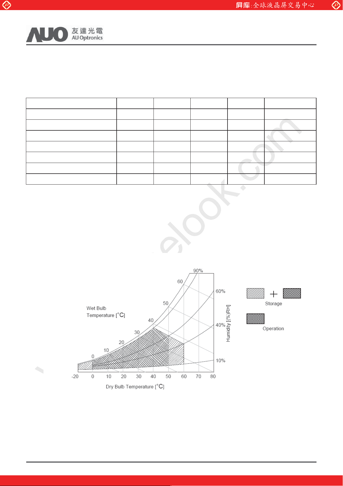
Operating Temperature TOP 0 +50 [oC] Note 2
Operating Humidity HOP 10 90 [%RH] Note 2
Storage Temperature TST -20 +60 [oC] Note 2
Storage Humidity HST 10 90 [%RH] Note 2
Panel Surface Temperature PST 65 [oC] Note 3
Note 1: Duration:50 msec.
Note 2 : Maximum Wet-Bulb should be 39 and No condensation.к
The relative humidity must not exceed 90% non-condensing at temperatures of 40 or less. At temperatures к
greater than 40 , the wet bк ulb temperature must not exceed 39 .к
Note 3: Surface temperature is measured at 50к Dry condition
© Copyright AUO Optronics Corp. 2011 All Rights Reserved. Page5 / 32
One step solution for LCD / PDP / OLED panel application: Datasheet, inventory and accessory!
www.panelook.com
Global LCD Panel Exchange Center
www.panelook.com
T420HVN01.3 Product Specification
3. Electrical Specification
The T420HVN01.3 requires two power inputs. One is employed to power the LCD electronics and to drive the TFT
array and liquid crystal. The other is to power Back Light Unit.
3.1 Electrical Characteristics
3.1.1: DC Characteristics
Rev.0.5
Parameter Symbol
Unit Note
Min. Typ. Max
LCD
Power Supply Input Voltage VDD 10.8 12 13.2 VDC
Power Supply Input Current IDD -- 0.89 1.2 A 1
Power Consumption PC -- -- 14.4 Watt 1
Value
Inrush Current I
Permissible Ripple of Power Supply Input Voltage
Input Differential Voltage
LVDS
Interface
Differential Input High Threshold Voltage VTH +100 -- +300 mVDC 4
Differential Input Low Threshold Voltage VTL -300 -- -100 mVDC 4
Input Common Mode Voltage V
CMOS
Interface
Input High Threshold Voltage
Input Low Threshold Voltage
Backlight Power Consumption P
-- -- 4 A 2
RUSH
*
V
V
-- --
RP
ЮV
Ю
ID
1.1 1.25 1.4 VDC 4
ICM
V
IH
(High)
V
IL
(Low)
BL
200 400 600 mV
2.7 -- 3.3 V
0 -- 0.6 V
-- 45.18 -- Watt
DD
5%
mV
pk-pk
4
DC
5
DC
5
DC
3
Life time (MTTF) 30000 Hour 8,9
© Copyright AUO Optronics Corp. 2011 All Rights Reserved. Page6 / 32
One step solution for LCD / PDP / OLED panel application: Datasheet, inventory and accessory!
www.panelook.com
Global LCD Panel Exchange Center
s
3.1.2: AC Characteristics
www.panelook.com
T420HVN01.3 Product Specification
Rev.0.5
Parameter Symbol
Receiver Clock : Spread Spectrum
Modulation range ʳ
Receiver Clock : Spread Spectrum
LVDS
Modulation frequencyʳ
Interface
Receiver Data Input Margin
Fclk = 85 MHz
Fclk = 65 MHzʳ
Note :
1. V
= 12.0V, Fv = 60Hz, Fclk= 74.25MHz , 25 , Test Pattern : White Patternк
DD
2. Measurement condition : Rising time = 400us
GND
10%
Value
Unit Note
Min. Typ. Max
Fclk_ssʳ
Fclk
-3%ʳ
--ʳ
Fclk
+3%ʳ
MHzʳ 5
Fssʳ 30ʳ --ʳ 200ʳ KHzʳ 5
tRMGʳ
90%
-0.4
-0.5ʳ
V
DD
--ʳ
--ʳ
0.4
0.5ʳ
nsʳ 7
3. Test Condition:
(1) The measure point of V
is in LCM side after connecting the System Board and LCM.
RP
(2) Under Max. Input current spec. condition
4. V
= 1.25V
ICM
LVDS -
V
ICM
LVDS +
GND
0V
400
|VID|
μ
V
TH
|VID|
V
TL
|VID|
© Copyright AUO Optronics Corp. 2011 All Rights Reserved. Page7 / 32
One step solution for LCD / PDP / OLED panel application: Datasheet, inventory and accessory!
www.panelook.com
Global LCD Panel Exchange Center
5. The measure points of V
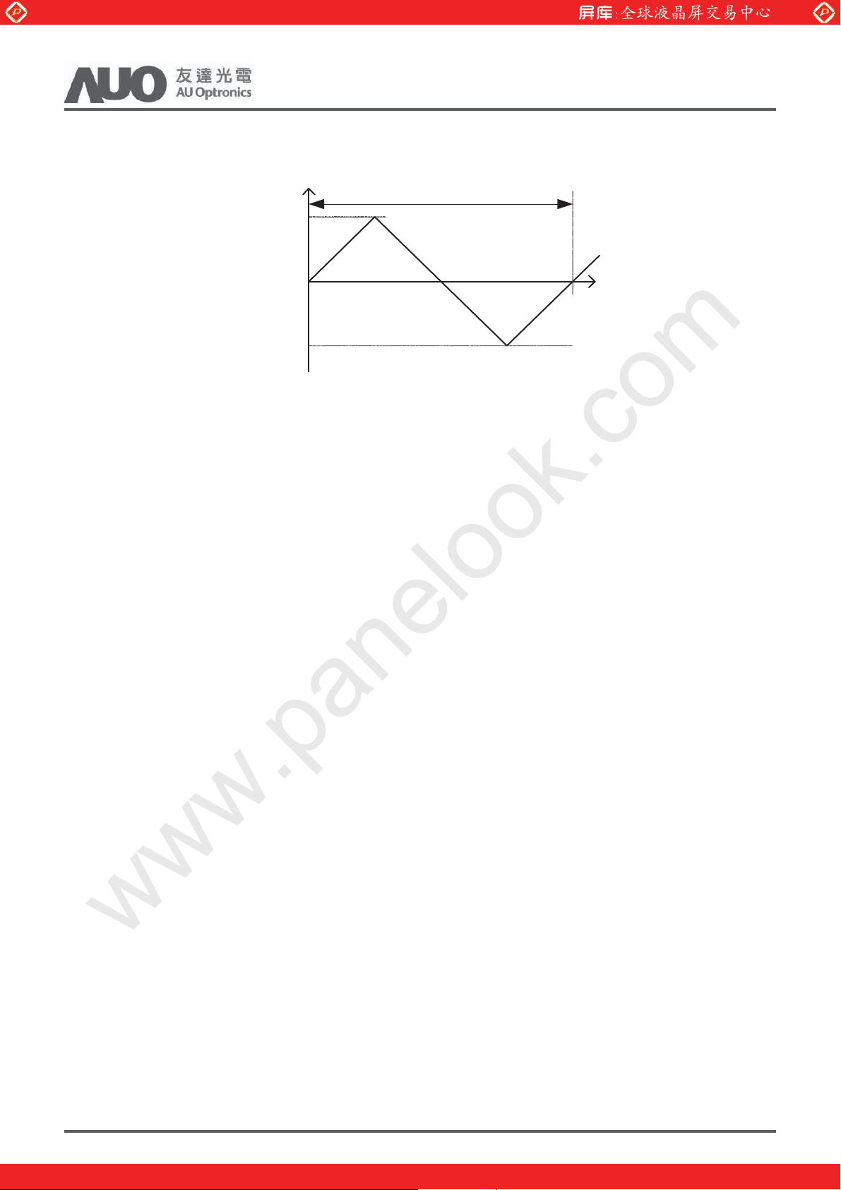
6. LVDS Receiver Clock SSCG (Spread spectrum clock generator) is defined as below figures
IH
Fclk_ss(max)
Fclk
Fclk_ss(min)
and V
www.panelook.com
T420HVN01.3 Product Specification
are in LCM side after connecting the System Board and LCM.
IL
1/F
SS
Rev.0.5
© Copyright AUO Optronics Corp. 2011 All Rights Reserved. Page8 / 32
One step solution for LCD / PDP / OLED panel application: Datasheet, inventory and accessory!
www.panelook.com
Global LCD Panel Exchange Center
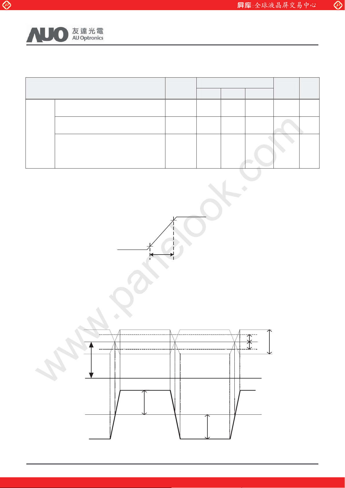
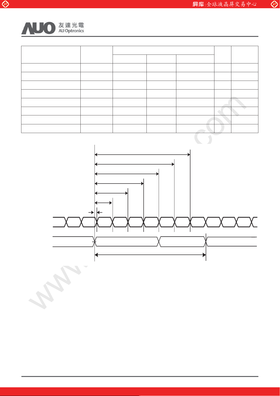
7. Receiver Data Input Margin
www.panelook.com
T420HVN01.3 Product Specification
Rev.0.5
Parameter Symbol
Min Type Max
Input Clock Frequency Fclk Fclk (min) -- Fclk (max) MHz T=1/Fclk
Input Data Position0 tRIP1 -|tRMG| 0 |tRMG| ns
Input Data Position1 tRIP0 T/7-|tRMG| T/7 T/7+|tRMG| ns
Input Data Position2 tRIP6 2T/7-|tRMG| 2T/7 2T/7+|tRMG| ns
Input Data Position3 tRIP5 3T/7-|tRMG| 3T/7 3T/7+|tRMG| ns
Input Data Position4 tRIP4 4T/7-|tRMG| 4T/7 4T/7+|tRMG| ns
Input Data Position5 tRIP3 5T/7-|tRMG| 5T/7 5T/7+|tRMG| ns
Input Data Position6 tRIP2 6T/7-|tRMG| 6T/7 6T/7+|tRMG| ns
Rating
Unit Note
tRIP2
tRIP3
tRIP4
tRIP5
tRIP6
tRIP0
tRIP1
LVDS-Rx
Input Data
Rx1 Rx0 Rx6 Rx5 Rx4 Rx3 Rx2 Rx 1 Rx0 Rx6Rx2Rx3
LVDS-Rx
V
= 0V
Input Cl ock
dif f
1/Fcl k=T
8. The relative humidity must not exceed 80% non-condensing at temperatures of 40к or less. At
temperatures greater than 40к, the wet bulb temperature must not exceed 39к. When operate at low
temperatures, the brightness of LED will drop and the life time of LED will be reduced.
9. The lifetime (MTTF) is defined as the time which luminance of LED is 50% compared to its original value.
[Operating condition: Continuous operating at Ta = 25±2к]
© Copyright AUO Optronics Corp. 2011 All Rights Reserved. Page9 / 32
One step solution for LCD / PDP / OLED panel application: Datasheet, inventory and accessory!
www.panelook.com
Global LCD Panel Exchange Center
www.panelook.com
T420HVN01.3 Product Specification
3.2 Interface Connections
LCD connector: 187059-51221-1 (P-TWO, LVDS connector)
187060-41221-1 (P-TWO, LVDS connector)
Mating connector:ʳʳ
PIN Symbol Description PIN Symbol Description
Rev.0.5
1 N.C. No connection 21
2 N.C. No connection 22
3 N.C. No connection 23
4 N.C. No connection 24
5 N.C. No connection 25
6 N.C. No connection 26
7 N.C. AUO Internal Use Only 27
8 N.C. No connection 28
9 GND Ground 29
CH3_0-
10
11
12
13
14
15
16
CH3_0+
CH3_1-
CH3_1+
CH3_2-
CH3_2+
GND
LVDS Channel 3, Signal 0- 30
LVDS Channel 3, Signal 0+ 31
LVDS Channel 3, Signal 1- 32
LVDS Channel 3, Signal 1+ 33
LVDS Channel 3, Signal 2- 34
LVDS Channel 3, Signal 2+ 35
Ground 36
CH3_3+
N.C.
N.C.
GND
GND
CH4_0-
CH4_0+
CH4_1-
CH4_1+
CH4_2-
CH4_2+
GND
CH4_CLK-
CH4_CLK+
GND
CH4_3-
LVDS Channel 3, Signal 3+
No connection
No connection
Ground
Ground
LVDS Channel 4, Signal 0-
LVDS Channel 4, Signal 0+
LVDS Channel 4, Signal 1-
LVDS Channel 4, Signal 1+
LVDS Channel 4, Signal 2-
LVDS Channel 4, Signal 2+
Ground
LVDS Channel 4, Clock -
LVDS Channel 4, Clock +
Ground
LVDS Channel 4, Signal 3-
17
18
19
20
ʳ
ʳ
CH3_CLK-
CH3_CLK+
GND
CH3_3-
LVDS Channel 3, Clock - 37
LVDS Channel 3, Clock + 38
Ground 39
LVDS Channel 3, Signal 3- 40 GND Ground
41 GND Ground
CH4_3+
N.C.
N.C.
LVDS Channel 4, Signal 3+
No connection
No connection
Note: N.C. : please leave this pin unoccupied. It can not be connected by any signal
(Low/GND/High).
© Copyright AUO Optronics Corp. 2011 All Rights Reserved. Page10 / 32
One step solution for LCD / PDP / OLED panel application: Datasheet, inventory and accessory!
www.panelook.com
 Loading...