

AUO T420HB01 V1 Specification
Global LCD Panel Exchange Center
Model Name: T420HB01 V1
( )Preliminary Specifications
(ϠϠϠϠ)Final Specifications
www.panelook.com
T420HB01 V1 Product Specification
Rev.1.3
Issue Date : 2011/07/20
Customer Signature Date AUO Date
Approved By
_________________________________
Note
Approval By PM Director
Yen Ting Chiu
_____________
Reviewed By RD Director
Eugene CC Chen
____________________________________
Reviewed By Project Leader
Kenney Chen
____________________________________
Prepared By PM
Shelby
____________________________________
© Copyright AUO Optronics Corp. 2011 All Rights Reserved. Page1 / 33
One step solution for LCD / PDP / OLED panel application: Datasheet, inventory and accessory!
www.panelook.com
Global LCD Panel Exchange Center
No
CONTENTS
RECORD OF REVISIONS
1 GENERAL DESCRIPTION
2 ABSOLUTE MAXIMUM RATINGS
3 ELECTRICAL SPECIFICATION
3-1 ELECTRIACL CHARACTERISTICS
3-2 INTERFACE CONNECTIONS
3-3 SIGNAL TIMING SPECIFICATION
www.panelook.com
T420HB01 V1 Product Specification
Rev.1.3
Contents
3-4 SIGNAL TIMING WAVEFORM
3-5 COLOR INPUT DATA REFERENCE
3-6 POWER SEQUENCE
3-7 BACKLIGHT SPECIFICATION
4 OPTICAL SPECIFICATION
5 MECHANICAL CHARACTERISTICS
6 RELIABILITY TEST ITEMS
7 INTERNATIONAL STANDARD
7-1 SAFETY
7-2 EMC
8 PACKING
8-1 DEFINITION OF LABEL
8-2 PACKING METHODS
8-3 PALLET AND SHIPMENT INFORMATION
9 PRECAUTION
9-1 MOUNTING PRECAUTIONS
9-2 OPERATING PRECAUTIONS
9-3 ELECTROSTATIC DISCHARGE CONTROL
9-4 PRECAUTIONS FOR STRONG LIGHT EXPOSURE
9-5 STORAGE
9-6 HANDLING PRECAUTIONS FOR PROTECT FILM
© Copyright AUO Optronics Corp. 2011 All Rights Reserved. Page2 / 33
One step solution for LCD / PDP / OLED panel application: Datasheet, inventory and accessory!
www.panelook.com
Global LCD Panel Exchange Center
Record of Revision
Version Date Page Description
0.0 2011/2/20 Pre-Spec First release
1.0 2011/05/02 Final-Spec First release
www.panelook.com
T420HB01 V1 Product Specification
Rev.1.3
1.1 2011/7/19 6 Update Power Supply Input Current
22
1.2 2011/7/20 24 Weight update to 8600 g
1.3 2011/7/22 31 Update Pallet and Shipment Information
30 Update PACKING METHODS
Update
[S1]
->0.45(typ.) , 1.68 (max)
+=
LL
),(),(3 WWLWWRLumD
© Copyright AUO Optronics Corp. 2011 All Rights Reserved. Page3 / 33
One step solution for LCD / PDP / OLED panel application: Datasheet, inventory and accessory!
www.panelook.com
Global LCD Panel Exchange Center
www.panelook.com
T420HB01 V1 Product Specification
1. General Description
This specification applies to the 42.0 inch Color TFT-LCD Module T420HB01 V1. This LCD module has a TFT
active matrix type liquid crystal panel 1,920x1,080 pixels, and diagonal size of 42.0 inch. This module supports
1,920x1,080 mode. Each pixel is divided into Red, Green and Blue sub-pixels or dots which are arranged in vertical
stripes. Gray scale or the brightness of the sub-pixel color is determined with a 8-bit gray scale signal for each dot.
The T420HB01 V1 has been designed to apply the 8-bit 2 channel LVDS interface method. It is intended to
support displays where high brightness, wide viewing angle, high color saturation, and high color depth are very
important. Also, 3D function is also embedded into front glass as pattern retarder.
Rev.1.3
* General Information
Items Specification Unit Note
Active Screen Size 42.00 inch
Display Area 930.24(H) x 523.26(V) mm
Outline Dimension 968.4(H) x 564 (V) x 20.9(D) mm D: front bezel to T-con cover
Driver Element a-Si TFT active matrix
Bezel Opening 939 (H) x 531 (V) mm
Display Colors 8 bit Colors
Number of Pixels 1,920x1,080 Pixel
Pixel Pitch 0.4845 mm
Pixel Arrangement RGB vertical stripe
Display Operation Mode Normally Black
Rotate Function Achievable Note 1
Note 1: Rotate Function refers to LCD display could be able to rotate.
© Copyright AUO Optronics Corp. 2011 All Rights Reserved. Page4 / 33
One step solution for LCD / PDP / OLED panel application: Datasheet, inventory and accessory!
www.panelook.com
Global LCD Panel Exchange Center
www.panelook.com
T420HB01 V1 Product Specification
Rev.1.3
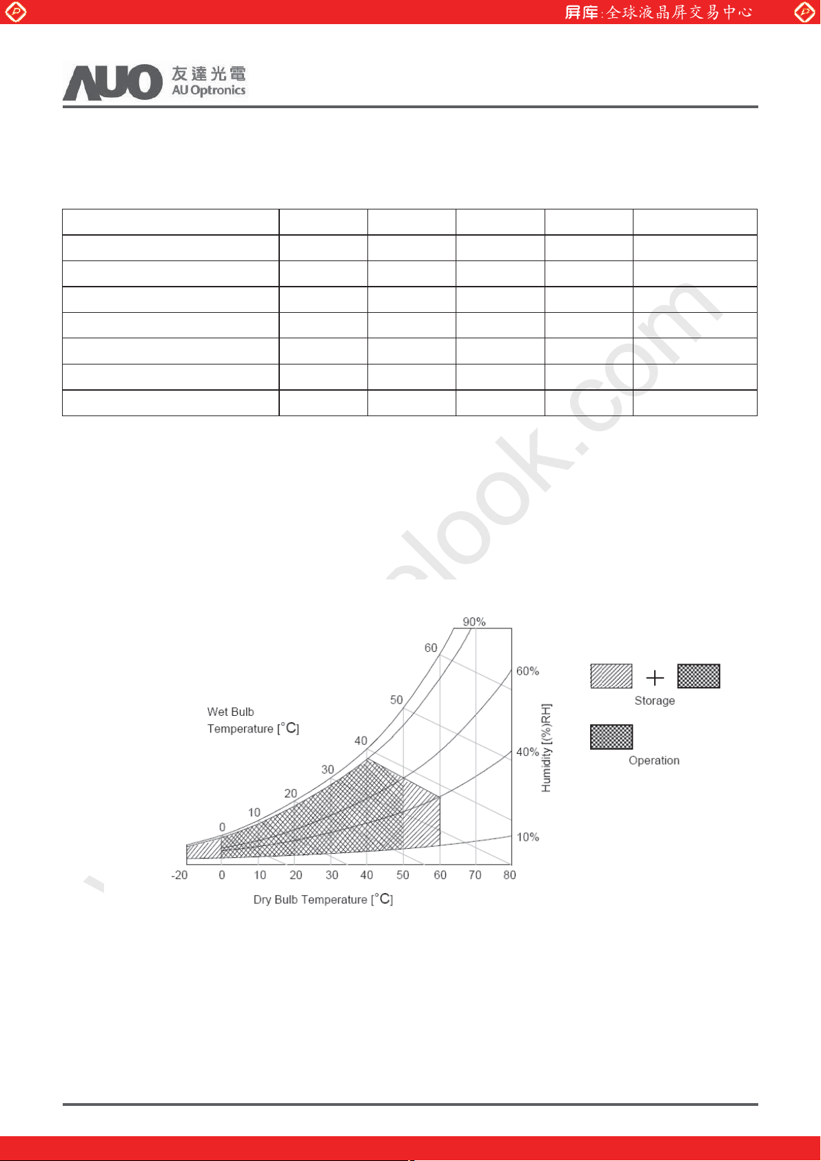
2. Absolute Maximum Ratings
The followings are maximum values which, if exceeded, may cause faulty operation or damage to the unit
Item Symbol Min Max Unit Conditions
Logic/LCD Drive Voltage Vcc -0.3 14 [Volt] Note 1
Input Voltage of Signal Vin -0.3 4 [Volt] Note 1
Operating Temperature TOP 0 +50 [oC] Note 2
Operating Humidity HOP 10 90 [%RH] Note 2
Storage Temperature TST -20 +60 [oC] Note 2
Storage Humidity HST 10 90 [%RH] Note 2
Panel Surface Temperature PST 65 [oC] Note 3
Note 1: Duration:50 msec.
Note 2 : Maximum Wet-Bulb should be 39 and No condensation.к
The relative humidity must not exceed 90% non-condensing at temperatures of 40 or less. At temperatures к
greater than 40 , the wet bulb temperature must not exceed 39 .кк
Note 3: Surface temperature is measured at 50к Dry condition
© Copyright AUO Optronics Corp. 2011 All Rights Reserved. Page5 / 33
One step solution for LCD / PDP / OLED panel application: Datasheet, inventory and accessory!
www.panelook.com
Global LCD Panel Exchange Center
www.panelook.com
T420HB01 V1 Product Specification
3. Electrical Specification
The T420HB01 V1 requires two power inputs. One is employed to power the LCD electronics and to drive the TFT
array and liquid crystal. The other is to power Back Light Unit.
3.1 Electrical Characteristics
3.1.1: DC Characteristics
Rev.1.3
Parameter Symbol
Unit Note
Min. Typ. Max
LCD
Value
Power Supply Input Voltage
Power Supply Input Current
Power Consumption
Inrush Current
[S4]
[S5]
Permissible Ripple of Power Supply Input Voltage
Input Differential Voltage
LVDS
Interface
Differential Input High Threshold Voltage VTH +100 -- +300 mVDC 4
Differential Input Low Threshold Voltage VTL -300 -- -100 mVDC 4
Input Common Mode Voltage V
CMOS
Interface
Input High Threshold Voltage
Input Low Threshold Voltage
Backlight Power Consumption
[S2]
VDD 10.8 12 13.2 VDC
[S3]
IDD -- 0.45 1.68 A 1
PC -- 5.4 20.16 Watt 1
I
-- -- 4 A 2
RUSH
*
V
DD
5%
mV
pk-pk
4
DC
5
DC
5
DC
[S6]
V
-- --
RP
ЮV
Ю
ID
1.1 1.25 1.4 VDC 4
ICM
V
IH
(High)
V
IL
(Low)
P
BL
200 400 600 mV
2.7 -- 3.3 V
0 -- 0.6 V
-- 69 73.2 Watt
3
© Copyright AUO Optronics Corp. 2011 All Rights Reserved. Page6 / 33
One step solution for LCD / PDP / OLED panel application: Datasheet, inventory and accessory!
www.panelook.com
Global LCD Panel Exchange Center
s
3.1.2: AC Characteristics
www.panelook.com
T420HB01 V1 Product Specification
Rev.1.3
Parameter Symbol
Input Channel Pair Skew Margin
Receiver Clock : Spread Spectrum
LVDS
Interface
Modulation range ʳ
Receiver Clock : Spread Spectrum
Modulation frequencyʳ
Receiver Data Input Margin
Fclk = 85 MHz
Fclk = 65 MHzʳ
Note :
1. V
= 12.0V, Fv = 60Hz, Fclk= 82MHz , 25 , Test Pattern : White Patternк
DD
2. Measurement condition : Rising time = 400us
[S7]
Value
Unit Note
Min. Typ. Max
t
SKEW (CP)
Fclk_ssʳ
-500 -- +500 ps 6
Fclk
-3%ʳ
--ʳ
Fclk
+3%ʳ
MHzʳ 7
Fssʳ 30ʳ --ʳ 200ʳ KHzʳ 7
ʳ
tRMGʳ -0.4
-0.5ʳ
V
90%
DD
--ʳ
--ʳ
0.4
0.5ʳ
nsʳ 8
GND
10%
3. Test Condition:
(1) The measure point of V
is in LCM side after connecting the System Board and LCM.
RP
(2) Under Max. Input current spec. condition.
4. V
= 1.25V
ICM
LVDS -
V
ICM
LVDS +
GND
0V
400
|VID|
μ
V
TH
|VID|
V
TL
|VID|
© Copyright AUO Optronics Corp. 2011 All Rights Reserved. Page7 / 33
One step solution for LCD / PDP / OLED panel application: Datasheet, inventory and accessory!
www.panelook.com
Global LCD Panel Exchange Center
5. The measure points of V
6. Input Channel Pair Skew Margin
Note: x = 0, 1, 2, 3, 4
IH
7. LVDS Receiver Clock SSCG (Spread spectrum clock generator) is defined as below figures
and V
www.panelook.com
T420HB01 V1 Product Specification
are in LCM side after connecting the System Board and LCM.
IL
Rev.1.3
Fclk_ss(max)
Fclk
Fclk_ss(min)
1/F
SS
© Copyright AUO Optronics Corp. 2011 All Rights Reserved. Page8 / 33
One step solution for LCD / PDP / OLED panel application: Datasheet, inventory and accessory!
www.panelook.com
Global LCD Panel Exchange Center
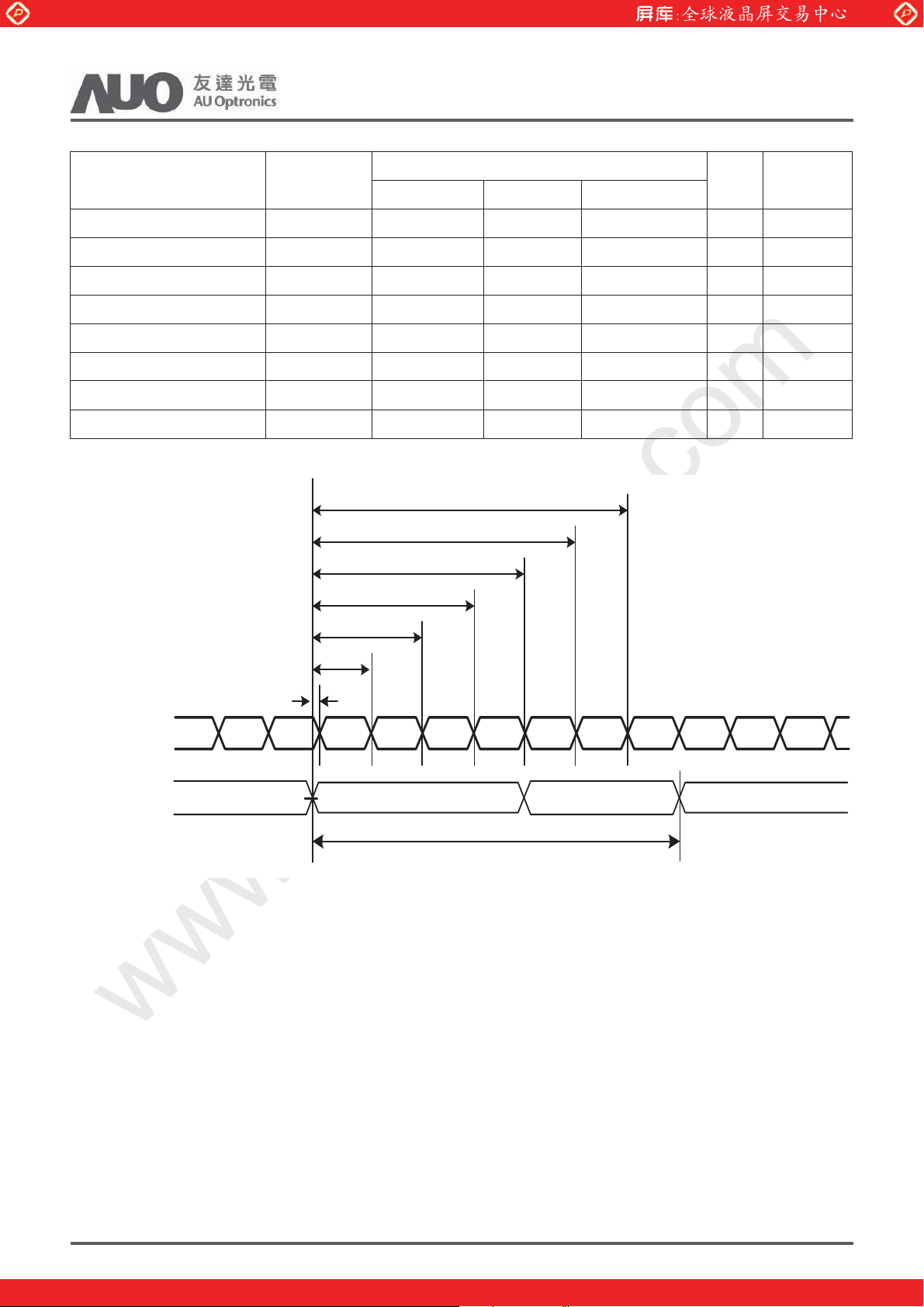
8. Receiver Data Input Margin
www.panelook.com
T420HB01 V1 Product Specification
Rev.1.3
Parameter Symbol
Min Type Max
Input Clock Frequency Fclk Fclk (min) -- Fclk (max) MHz T=1/Fclk
Input Data Position0 tRIP1 -|tRMG| 0 |tRMG| ns
Input Data Position1 tRIP0 T/7-|tRMG| T/7 T/7+|tRMG| ns
Input Data Position2 tRIP6 2T/7-|tRMG| 2T/7 2T/7+|tRMG| ns
Input Data Position3 tRIP5 3T/7-|tRMG| 3T/7 3T/7+|tRMG| ns
Input Data Position4 tRIP4 4T/7-|tRMG| 4T/7 4T/7+|tRMG| ns
Input Data Position5 tRIP3 5T/7-|tRMG| 5T/7 5T/7+|tRMG| ns
Input Data Position6 tRIP2 6T/7-|tRMG| 6T/7 6T/7+|tRMG| ns
Rating
Unit Note
tRIP2
tRIP3
tRIP4
tRIP5
LVDS-Rx
Input Data
LVDS-Rx
Input Cl ock
tRIP6
tRIP0
tRIP1
Rx1 Rx0 Rx6 Rx5 Rx4 Rx3 Rx2 Rx 1 Rx0 Rx6Rx2Rx3
V
= 0V
dif f
1/Fcl k=T
© Copyright AUO Optronics Corp. 2011 All Rights Reserved. Page9 / 33
One step solution for LCD / PDP / OLED panel application: Datasheet, inventory and accessory!
www.panelook.com
Global LCD Panel Exchange Center
www.panelook.com
T420HB01 V1 Product Specification
Rev.1.3
3.2 Interface Connections
LCD connector: 187059-51221 (P-TWO, LVDS connector)
3.3
PIN Symbol Description PIN Symbol Description
1 N.C. AUO Internal Use Only 26 GND Ground
2 N.C. AUO Internal Use Only 27 GND Ground
3 N.C. AUO Internal Use Only 28 CH2_0- LVDS Channel 2, Signal 04 N.C. AUO Internal Use Only 29 CH2_0+ LVDS Channel 2, Signal 0+
3D Function Enable
53D_EN
High(3.3V) : 3D
Open/Low(GND) : 2D
Panel Rotation Display Control
6ROTATE
High(3.3V) : Rotate Enable
Open/Low(GND) : Rotate Disable
7 LVDS_SEL
Open/High(3.3V) for NS,
Low(GND) for JEIDA
8 N.C. AUO Internal Use Only 33 CH2_2+ LVDS Channel 2, Signal 2+
9 N.C. AUO Internal Use Only 34 GND Ground
10 N.C. AUO Internal Use Only 35 CH2_CLK- LVDS Channel 2, Clock 11 GND Ground 36 CH2_CLK+ LVDS Channel 2, Clock +
12 CH1_0- LVDS Channel 1, Signal 0- 37 GND Ground
13 CH1_0+ LVDS Channel 1, Signal 0+ 38 CH2_3- LVDS Channel 2, Signal 314 CH1_1- LVDS Channel 1, Signal 1- 39 CH2_3+ LVDS Channel 2, Signal 3+
15 CH1_1+ LVDS Channel 1, Signal 1+ 40 CH2_4- LVDS Channel 2, Signal 416 CH1_2- LVDS Channel 1, Signal 2- 41 CH2_4+ LVDS Channel 2, Signal 4+
17 CH1_2+ LVDS Channel 1, Signal 2+ 42 GND Ground
18 GND Ground 43 GND Ground
19 CH1_CLK- LVDS Channel 1, Clock - 44 GND Ground
20 CH1_CLK+ LVDS Channel 1, Clock + 45 GND Ground
21 GND Ground 46 GND Ground
22 CH1_3- LVDS Channel 1, Signal 3- 47 NC No connection
23 CH1_3+ LVDS Channel 1, Signal 3+ 48 V
24 CH1_4- LVDS Channel 1, Signal 4- 49 V
25 CH1_4+ LVDS Channel 1, Signal 4+ 50 V
51 V
Note: N.C. : please leave this pin unoccupied. It can not be connected by any signal
30 CH2_1- LVDS Channel 2, Signal 1-
31 CH2_1+ LVDS Channel 2, Signal 1+
32 CH2_2- LVDS Channel 2, Signal 2-
DD
DD
DD
DD
Power Supply, +12V DC Regulated
Power Supply, +12V DC Regulated
Power Supply, +12V DC Regulated
Power Supply, +12V DC Regulated
(Low/GND/High)
© Copyright AUO Optronics Corp. 2011 All Rights Reserved. Page10 / 33
One step solution for LCD / PDP / OLED panel application: Datasheet, inventory and accessory!
www.panelook.com
 Loading...