

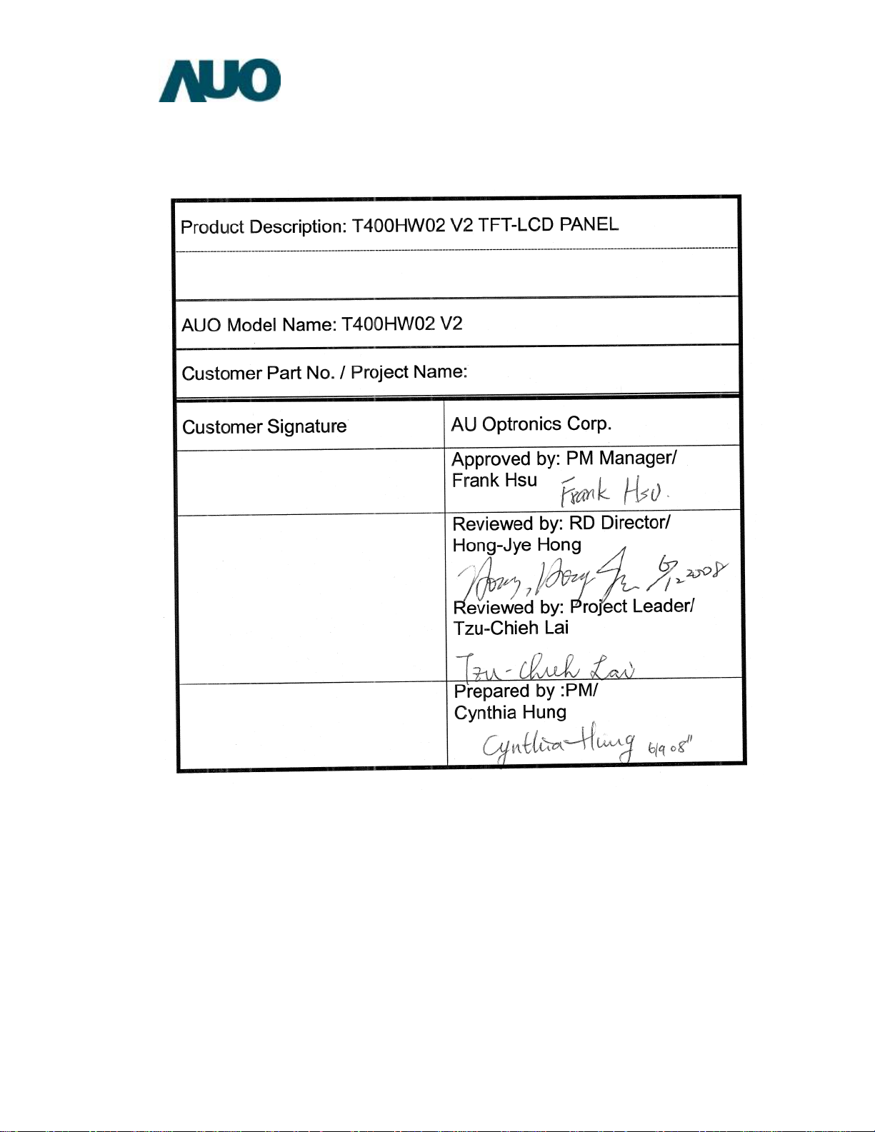
AUO T400HW02 V2 Specification
©Copyright AU Optronics Corp.
2007 All Rights Reserved. T400HW02 V2 Ver3/28 1
No Reproduction and Redistribution Allowed

Document Version: 3.0
Date:2009/04/27
Product Specifications
40” Full HD Color TFT-LCD Module
Model Name: T400HW02 V2
() Preliminary Specifications
(*) Final Specifications
©Copyright AU Optronics Corp.
2007 All Rights Reserved. T400HW02 V2 Ver3 2
No Reproduction and Redistribution Allowed
Contents
No
CONTENTS
RECORD OF REVISIONS
1 GENERAL DESCRIPTION
2 ABSOLUTE MAXIMUM RATINGS
3 ELECTRICAL SPECIFICATION
3-1 ELECTRIACL CHARACTERISTICS
3-2 INTERFACE CONNECTIONS
3-3 SIGNAL TIMING SPECIFICATION
3-4 SIGNAL TIMING WAVEFORM
3-5 COLOR INPUT DATA REFERENCE
3-6 POWER SEQUENCE
3-7 BACK LIGHT POWER SPECIFICATION
4 OPTICAL SPECIFICATION
5 MECHANICAL CHARACTERISTICS
6 RELIABILITY TEST ITEMS
7 INTERNATIONAL STANDARD
8 PACKING
9 PRECAUTION
©Copyright AU Optronics Corp.
2007 All Rights Reserved. T400HW02 V2 Ver3 3
No Reproduction and Redistribution Allowed
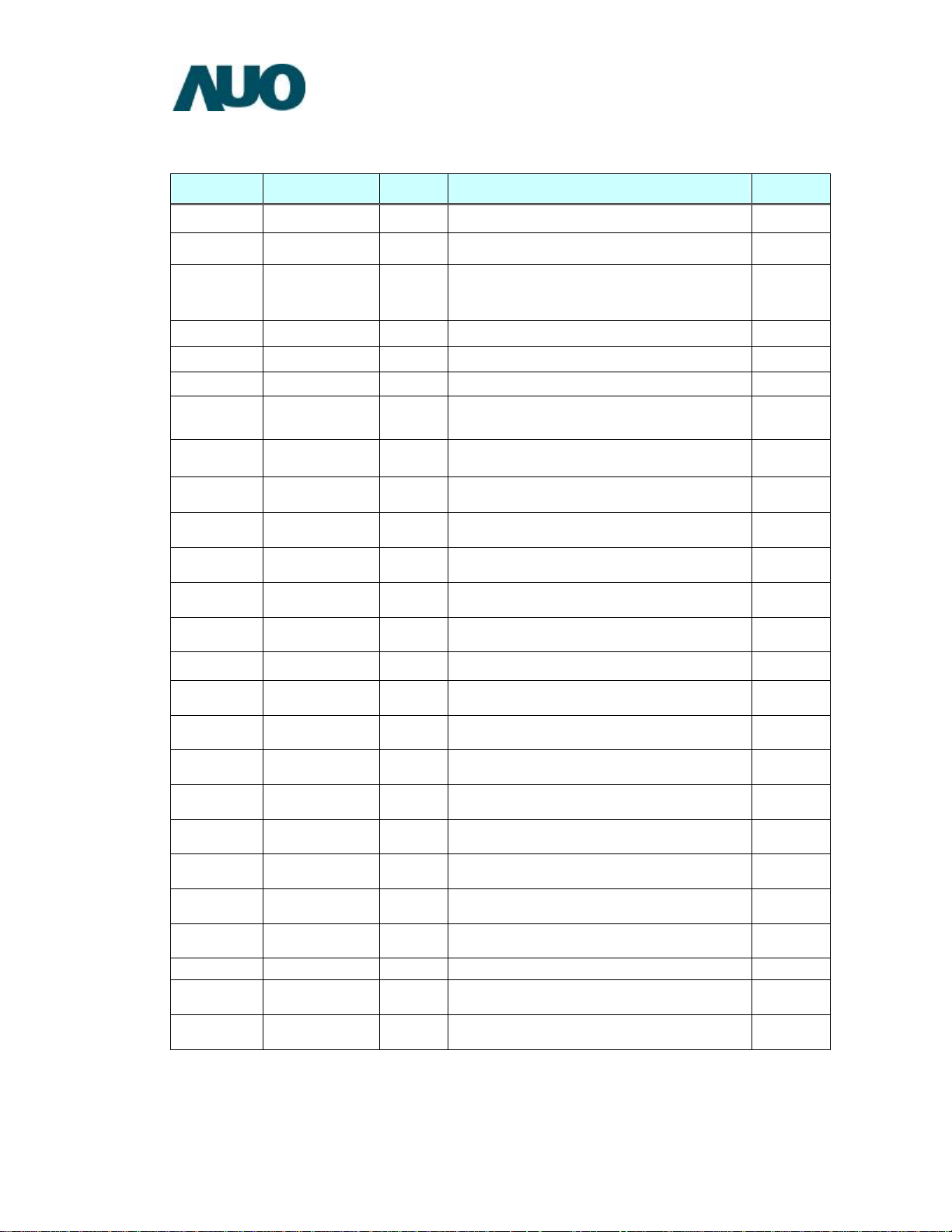
Record of Revision
Version Data No. Description Remark
1.0 2008/4/30 First release
2.0 2008/6/09 1
2
3 Update section 4, response time definition
3.0 2009/04/27 1 Update section 3.7.2, CN2 polarity
Update section 3-7.3, I
nge to IL=9.7mA)
Update section 3-7.3, lamp striking voltage
from 1600 to 1355 (25℃), from 1900 to
1625 (0℃)
4 Update section 4, response time spec
5 Update section 6, reliability condition
Spec (IL=10.5mA cha
T
N/A
©Copyright AU Optronics Corp.
2007 All Rights Reserved. T400HW02 V2 Ver3 4
No Reproduction and Redistribution Allowed
1. General Description
This specification applies to the 40.0 inch Color TFT-LCD Module T400HW02 V2. This LCD
module has a TFT active matrix type liquid crystal panel 1,920x1,080 pixels, and diagonal size of 40.0
inch. This module supports 1,920x1,080 mode. Each pixel is divided into Red, Green and Blue
sub-pixels or dots which are arranged in vertical stripes. Gray scale or the brightness of the sub-pixel
color is determined with a 8-bit gray scale signal for each dot.
The T400HW02 V2 has been designed to apply the 8-bit 2 channel LVDS interface method. It is
intended to support displays where high brightness, wide viewing angle, high color saturation, and
high color depth are very important.
* General Information
Items Specification Unit Note
Active Screen Size 40.00 inch
Display Area 885.6(H) x 498.15(V) mm
Outline Dimension 952.0(H) x 551.0 (V) x 53.2(D) mm With Balance board
Driver Element a-Si TFT active matrix
Display Colors 8 bit, 16.7M Colors
Number of Pixels
Pixel Pitch 0.46125 (H) x 0.46125(W) mm
Color Gamut 72 % NTSC
Pixel Arrangement RGB vertical stripe
Display Operation Mode Normally Black
Surface Treatment
Hard-Coating(3H),Haze=11%
1,920x1,080 Pixel
Anti-Glare,
©Copyright AU Optronics Corp.
2007 All Rights Reserved. T400HW02 V2 Ver3 5
No Reproduction and Redistribution Allowed
2. Absolute Maximum Ratings
The followings are maximum values which, if exceeded, may cause faulty operation or damage to the
unit
Item Symbol
Logic/LCD Drive Voltage V
-0.3 14.0 V
DD
Input Voltage of Signal Vin -0.3 3.6 V
Min. Max Unit Note
1
DC
1
DC
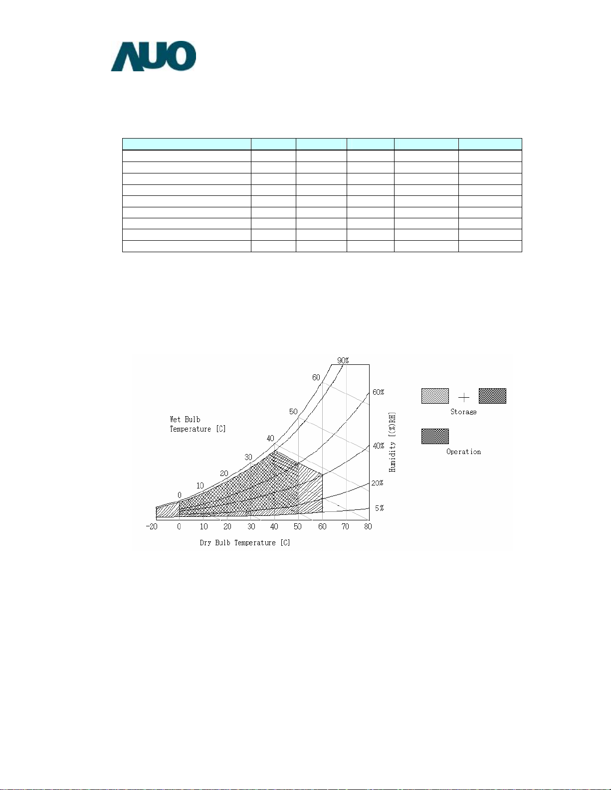
Operating Temperature TOP 0 +50 °C 2
Operating Humidity HOP 10 90 %RH 2
Storage Temperature TST -20 +60 °C 2
Storage Humidity HST 10 90 %RH 2
Shock (non-operation) ±x, ±y -- 50 G 3
Shock (non-operation) ±z -- 50 G 3
Vibration (non-operation) -- 1.5 G 4
Note 1: Duration = 50ms
Note 2: Maximum Wet-Bulb should be 39°C and No condensation.
Note 3: Sine wave, 11ms, direction: ±x, ±y, ±z (one time each direction)
Note 4: Wave form: random, vibration level: 1.5G RMS, Bandwidth: 10--300Hz
Duration: X, Y, Z 30min (one time each direction)
©Copyright AU Optronics Corp.
2007 All Rights Reserved. T400HW02 V2 Ver3 6
No Reproduction and Redistribution Allowed

3. Electrical Specification
The T400HW02 V2 requires two power inputs. One is employed to power the LCD electronics and to
drive the TFT array and liquid crystal. The second input, which powers the CCFL, is typically
generated by an integrate power (I/P) system.
3.1 Electrical Characteristics
Parameter Symbol
Power Supply Input Voltage V
Power Supply Input Current I
Power Consumption P
Inrush Current I
Differential Input
High Threshold
Voltage
LVDS
Interface
CMOS
Interface
Backlight Power Consumption P
Life Time 50000 60000
The performance of the Lamp in LCD panel, for example life time or brightness, is extremely
influenced by the characteristics of the balance board and I/P board. All the parameters should be
carefully designed as not to produce too much leakage current from high-voltage output. While
design or order balance board, please make sure unwanted lighting caused by the mismatch of
the lamp and balance board (no lighting, flicker, etc) never occurs. After confirmation, the LCD
Panel should be operated in the same condition as installed in your instrument.
Differential Input
Low Threshold
Voltage
Common Input
Voltage
Input High
Threshold Voltage
Input Low
Threshold Voltage
DD
DD
C
RUSH
VTH -- -- +100 mVDC 4
VTL -100 -- -- mVDC 4
V
CIM
VIH
(High)
VIL
(Low)
BL
Min. Typ. Max
10.8 12 13.2 VDC
-- 1.2 1.6 A 1
-- 14.4 19.2 Watt 1
-- -- 4.5 A 5
1.10 1.25 1.40 VDC
2.4 -- 3.3 VDC
0 -- 0.7 VDC
150 160 170 Watt 2
Value
Unit Note
-- Hours 3
©Copyright AU Optronics Corp.
2007 All Rights Reserved. T400HW02 V2 Ver3 7
No Reproduction and Redistribution Allowed
s
µ
Do not attach a conducting tape to lamp connecting wire. If the lamp wire attach to conducting
tape, TFT-LCD Module has a low luminance and the inverter has abnormal action, because
leakage current occurs between lamp wire and conducting tape.
The relative humidity must not exceed 80% non-condensing at temperatures of 40 °C or less. At
temperatures greater than 40°C the wet bulb temperature must not exceed 39°C. When operate
at low temperatures, the brightness of CCFL will drop and the lifetime of CCFL will be reduced.
Note:
1. VDD=12.0V, fV=60Hz, fCLK=81.5Mhz, 25°C, VDD duration time=400µs, test pattern: white pattern
2. The power consumption shown above is tested by lamp current IL=9.7mA and used by IP JIG.
3. The life is determined as the time at which luminance of the lamp is 50% compared to that of
initial value at the typical lamp current on condition of continuous operating at 25 ±2°C.
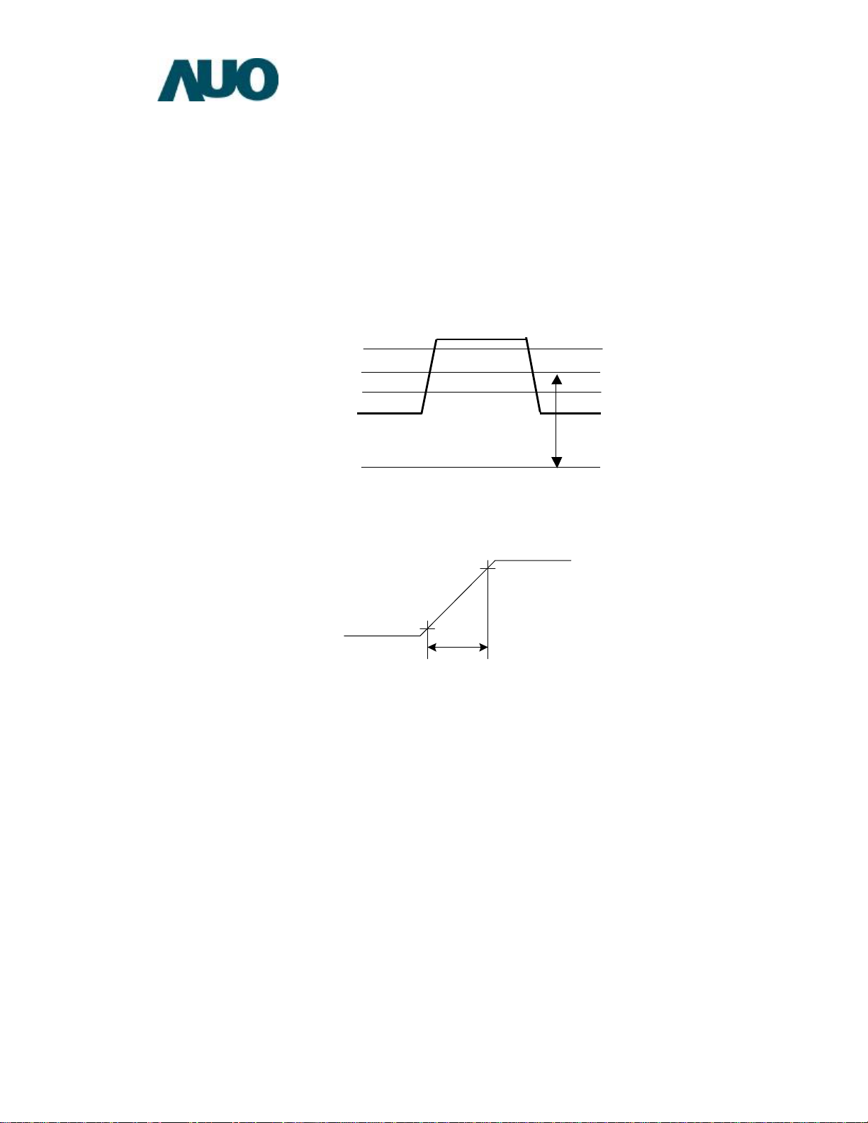
4. V
=1.25V
CIM
VTH
VCIM
VTL
0V
Figure: LVDS Differential Voltage
5. Measurement condition: rising time=400 µs
GND
0.1 Vdd
400
0.9 Vdd
Vdd
©Copyright AU Optronics Corp.
2007 All Rights Reserved. T400HW02 V2 Ver3 8
No Reproduction and Redistribution Allowed
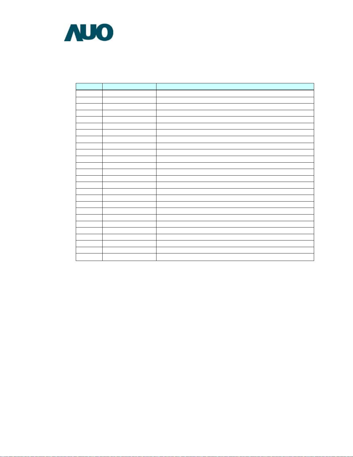
3.2 Interface Connections
l LCD connector: FI-RE51S-HF (JAE)
l Mating connector: FI-RE51S-HL (JAE)
PIN # Signal Name Description
1 V
2 V
3 V
4 V
5 V
6 GND Ground
7 GND Ground
8
9 GND Ground
10 RO_0- Negative(-) LVDS differential data input
11 RO_0+ Positive(+) LVDS differential data input
12 RO_1- Negative(-) LVDS differential data input
13 RO_1+ Positive(+) LVDS differential data input
14 RO_2- Negative(-) LVDS differential data input
15 RO_2+ Positive(+) LVDS differential data input
16 GND Ground
17 RO_CLK- Clock Signal(-)
18 RO_CLK+ Clock Signal(+)
19 GND Ground
20 RO_3- Negative(-) LVDS differential data input
21 RO_3+ Positive(+) LVDS differential data input
22 NC No connection
23 NC No connection
24 GND Ground
25 RE_0- Negative(-) LVDS differential data input
26
12V power supply
DD
12V power supply
DD
12V power supply
DD
12V power supply
DD
12V power supply
DD
GND
RE_0+
Ground
Positive(+) LVDS differential data input
©Copyright AU Optronics Corp.
2007 All Rights Reserved. T400HW02 V2 Ver3 9
No Reproduction and Redistribution Allowed
 Loading...