

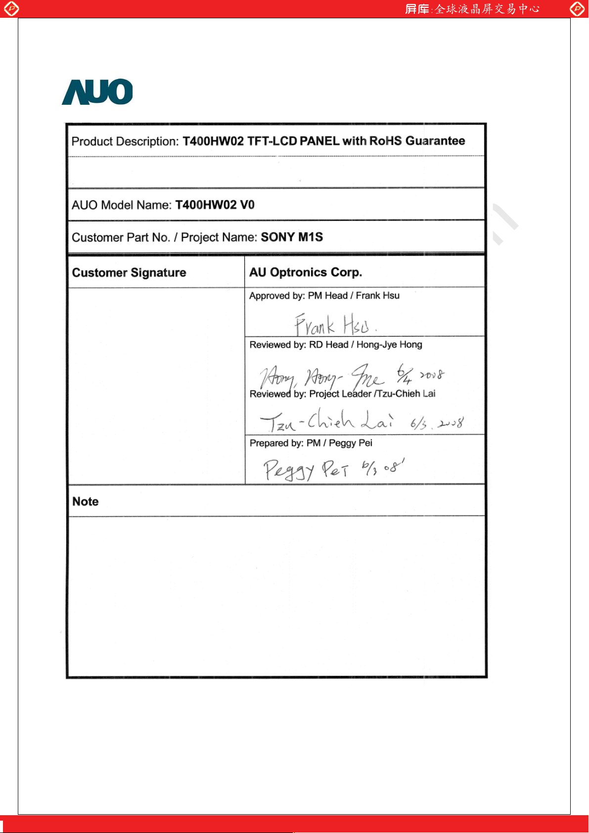
AUO T400HW02 V0 Specification
Global LCD Panel Exchange Center
www.panelook.com
©Copyright AU Optronics Corp.
2007 All Rights Reserved. T400HW02 V0
No Reproduction and Redistribution Allowed
One step solution for LCD / PDP / OLED panel application: Datasheet, inventory and accessory!
ʳ
1/32
www.panelook.com
Global LCD Panel Exchange Center
www.panelook.com
Document Version: 1.1
Date: 2008/06/11
Product Functional Specification
40" Full HD Color TFT-LCD Module
Model Name: T400HW02 V0
() Preliminary Specification
(*) Final Specification
©Copyright AU Optronics Corp.
2007 All Rights Reserved. T400HW02 V0
No Reproduction and Redistribution Allowed
One step solution for LCD / PDP / OLED panel application: Datasheet, inventory and accessory!
ʳ
2/32
www.panelook.com

Global LCD Panel Exchange Center
www.panelook.com
Contents
No
CONTENTS
RECORD OF REVISIONS
1 GENERAL DESCRIPTION
2 ABSOLUTE MAXIMUM RATINGS
3 ELECTRICAL SPECIFICATION
3-1 ELECTRIACL CHARACTERISTICS
3-2 INTERFACE CONNECTOR
3-3 SIGNAL TIMING SPECIFICATION
3-4 SIGNAL TIMING WAVEFORM
3-5 COLOR INPUT DATA REFERENCE
3-6 POWER SEQUENCE
3-7 BACK LIGHT POWER SPECIFICATION
4 OPTICAL SPECIFICATION
5 MECHANICAL CHARACTERISTICS
6 INTERNATIONAL STANDARD
7 PACKING
8 PRECAUTION
9 RELIABILITY
Appendix A EMI Criteria
©Copyright AU Optronics Corp.
2007 All Rights Reserved. T400HW02 V0
No Reproduction and Redistribution Allowed
One step solution for LCD / PDP / OLED panel application: Datasheet, inventory and accessory!
ʳ
3/32
www.panelook.com

Global LCD Panel Exchange Center
Record of Revision
Version Data Page. Items New Description Remark
1.0 2008/6/04 -- First release N/A
1.1 2008/06/11 28 Update panel label content
www.panelook.com
©Copyright AU Optronics Corp.
2007 All Rights Reserved. T400HW02 V0
No Reproduction and Redistribution Allowed
One step solution for LCD / PDP / OLED panel application: Datasheet, inventory and accessory!
ʳ
4/32
www.panelook.com
Global LCD Panel Exchange Center
1. General Description
This specification applies to the 40 inch Color TFT-LCD Module T400HW02 V0. This LCD module has a TFT
active matrix type liquid crystal panel 1920x1080 pixels, and diagonal size of 40 inch. This module supports Full
HD mode (Non-interlace).
Each pixel is divided into Red, Green and Blue sub-pixels or dots which are arranged in vertical stripes. Gray
scale or the brightness of the sub-pixel color is determined with a 10-bit gray scale signal for each dot.
The T400HW02 V0 has been designed to apply the 10-bit 2-channel LVDS interface method. It is intended to
support displays where high brightness, Hi Color Gamut (92% NTSC), wide viewing angle, and high color depth
are very important.
The T400HW02 V0 backlight unit is using inverter-less solution (inductor type balance board), and need to be
powered by integrated power system by customers.
www.panelook.com
*
General Information
Items Specification Unit Note
Active Screen Size 40 inches Diagonal
Display Area 885.6(H) x 498.15(V) mm
Outline Dimension 930.6(H) x 542.8(V) x 53.1(D) mm With Balance Board
Driver Element a-Si TFT active matrix
Display Colors 1073.7M colors
Color Gamut 92 % NTSC
Number of Pixels 1920 x 1080 pixel
Pixel Arrangement RGB vertical stripe
Pixel Pitch 0.46125 mm
Display Mode Normally Black
Surface Treatment AG, Haze 11%,3H
RoHS RoHS compliance
©Copyright AU Optronics Corp.
2007 All Rights Reserved. T400HW02 V0
No Reproduction and Redistribution Allowed
One step solution for LCD / PDP / OLED panel application: Datasheet, inventory and accessory!
ʳ
5/32
www.panelook.com
Global LCD Panel Exchange Center
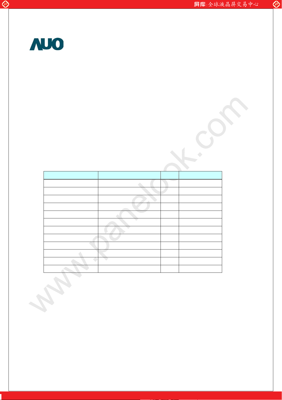
2. Absolute Maximum Ratings
The followings are maximum values which, if exceeded, may cause faulty operation or damage to the unit
Item Symbol Min. Max Unit Note
Logic/LCD Drive Voltage VDD -0.3 14.0 VDC 1
Input Voltage of Signal VIN -0.3 3.5 VDC 1
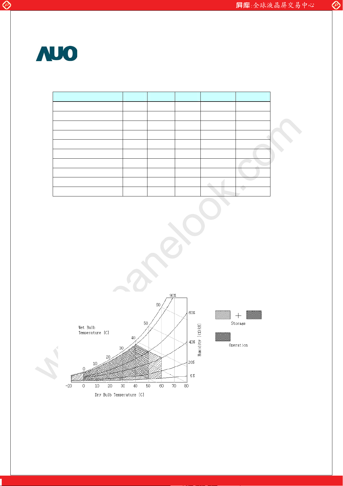
Operating Temperature TOP 0 +50 °C 2
Operating Humidity HOP 10 90 %RH 2
Storage Temperature TST -20 +60 °C 2
Storage Humidity HST 10 90 %RH 2
Panel Surface Temperature T
Shock (non-operation) ±x, ±y -- 50 G 3
Shock (non-operation) ±z -- 50 G 3
Vibration (non-operation) -- 1.5 G 4
www.panelook.com
-- +65 °C 2
SUR
Note 1: Duration = 50ms
Note 2: Maximum Wet-Bulb should be 39°C and no condensation. The relative humidity must not exceed
90% non-condensing at temperatures of 40°C or less. At temperatures greater than 40°C, the wet
bulb temperature must not exceed 39°C.
Note 3: Sine wave, 11ms, direction: ±x, ±y, ±z (one time each direction)
Note 4: Wave form: random, vibration level: 1.5G RMS, Bandwidth: 10--300Hz
Duration: X, Y, Z 30min (one time each direction)
©Copyright AU Optronics Corp.
2007 All Rights Reserved. T400HW02 V0
No Reproduction and Redistribution Allowed
One step solution for LCD / PDP / OLED panel application: Datasheet, inventory and accessory!
ʳ
6/32
www.panelook.com
Global LCD Panel Exchange Center
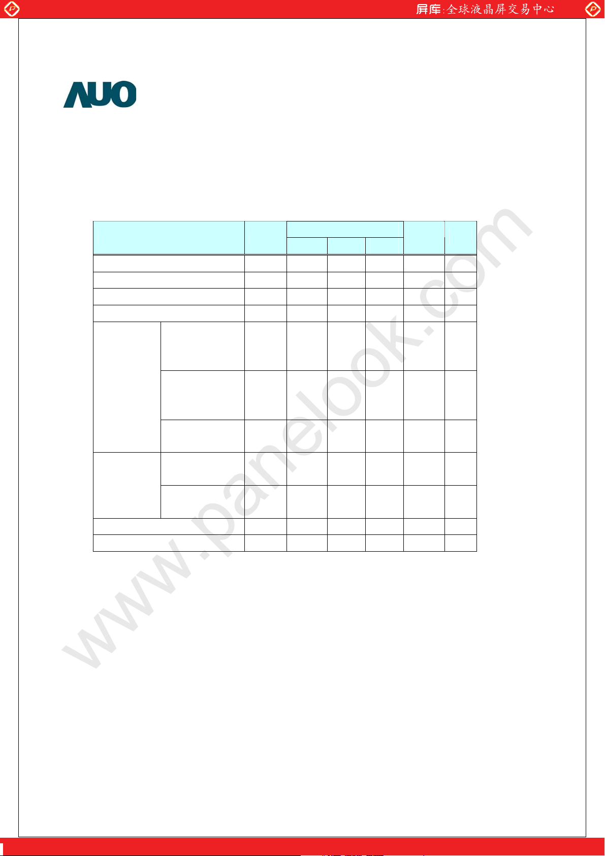
3. Electrical Specification
The T400HW02 requires two power inputs. One is employed to power the LCD electronics and to drive the TFT
array and liquid crystal. The second input, which powers the CCFL, is typically generated by an integrate power
(I/P) system.
3.1 Electrical Characteristics
Parameter Symbol
Power Supply Input Voltage VDD 10.8 12.0 13.2 VDC
Power Supply Input Current IDD -- 1.6 3.0 A 1
Power Consumption PDD -- 19.2 39.6 Watt 1
Inrush Current I
Differential Input
High Threshold
Voltage
LVD S
Interface
CMOS
Interface
Backlight Power Consumption PBL 120 145 170 Watt 2
Life Time 30,000 -- -- Hours 3
The performance of the Lamp in LCD panel, for example life time or brightness, is extremely influenced by
the characteristics of the balance board and I/P board. All the parameters should be carefully designed as
not to produce too much leakage current from high-voltage output. While design or order balance board,
please make sure unwanted lighting caused by the mismatch of the lamp and balance board (no lighting,
flicker, etc) never occurs. After confirmation, the LCD Panel should be operated in the same condition as
installed in your instrument.
Do not attach a conducting tape to lamp connecting wire. If the lamp wire attach to conducting tape,
TFT-LCD Module has a low luminance and the inverter has abnormal action, because leakage current
occurs between lamp wire and conducting tape.
Differential Input
Low Threshold
Voltage
Common Input
Voltage
Input High
Threshold Voltage
Input Low
Threshold Voltage
www.panelook.com
Valu e
Min. Typ. Max
-- -- 8 A 5
RUSH
V
-- -- +100 mVDC 4
TH
V
-100 -- -- mVDC 4
TL
V
1.10 1.2 1.40 VDC
CIM
VIH
-- -- 2.1 V
(High)
V
IL
(Low)
0.7 -- -- V
Unit Note
DC
DC
©Copyright AU Optronics Corp.
2007 All Rights Reserved. T400HW02 V0
No Reproduction and Redistribution Allowed
One step solution for LCD / PDP / OLED panel application: Datasheet, inventory and accessory!
ʳ
7/32
www.panelook.com
Global LCD Panel Exchange Center
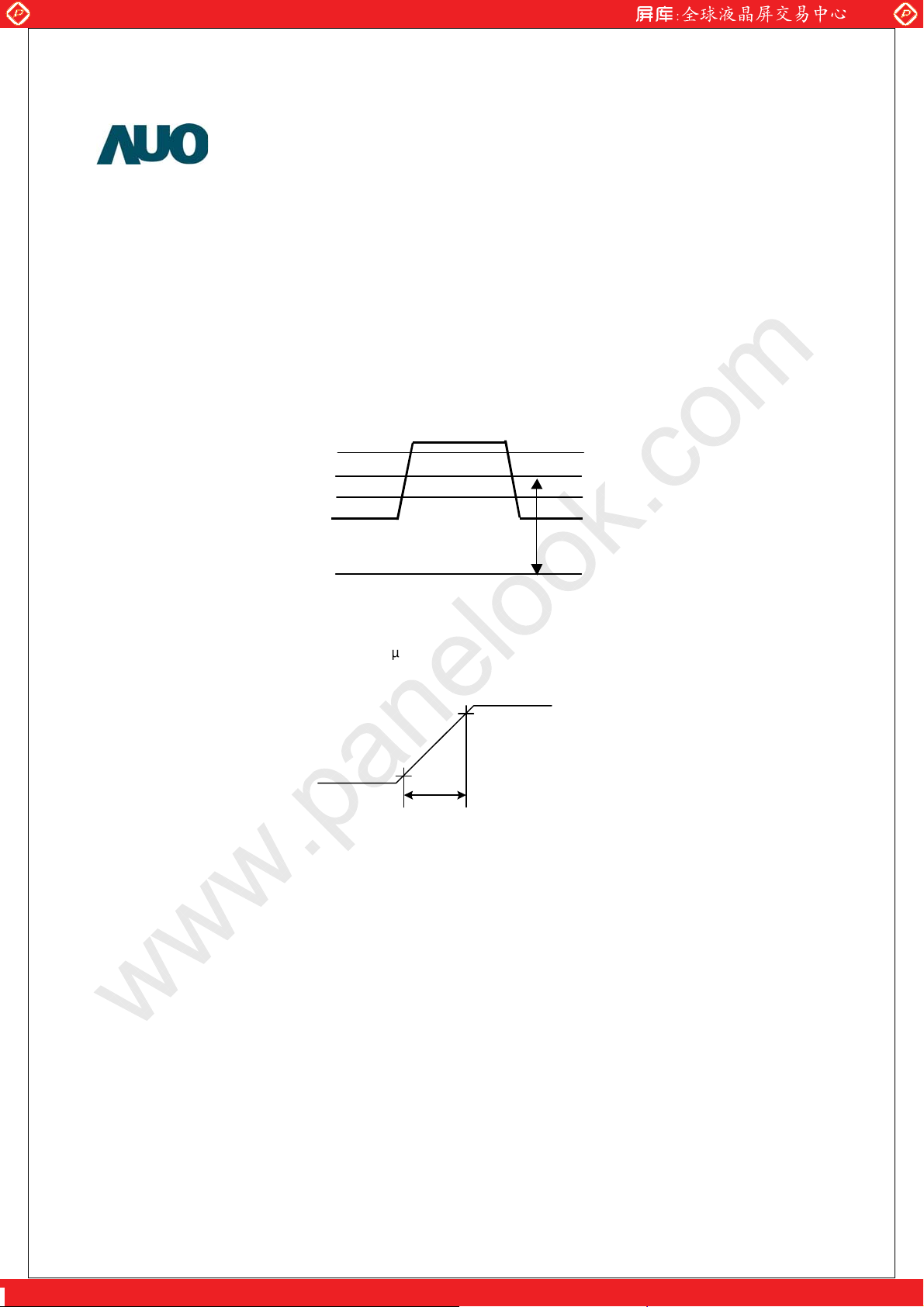
μ
The relative humidity must not exceed 80% non-condensing at temperatures of 40°C or less. At
temperatures greater than 40°C the wet bulb temperature must not exceed 39°C. When operate at low
temperatures, the brightness of CCFL will drop and the lifetime of CCFL will be reduced.
Note:
1. V
2. The backlight power consumption does not include loss of external power system. After the backlight
3. The life is determined as the time at which luminance of the lamp is 50% compared to that of initial value
4. V
=12.0V, fV=60Hz, f
DD
unit has been ‘ON’ for 2 hours.
at the typical lamp current on condition of continuous operating at 25±2°C.
=1.2V
CIM
CLK
=75Mhz, 25°C, VDD duration time=470μs, test pattern: full white pattern
VTH
www.panelook.com
VCIM
VTL
0V
5. Measurement condition: rising time=470
GND
Figure: LVDS Differential Voltage
ʦ
μs
0.9 Vdd
0.1 Vdd
s
400
470μs
Vdd
©Copyright AU Optronics Corp.
2007 All Rights Reserved. T400HW02 V0
No Reproduction and Redistribution Allowed
One step solution for LCD / PDP / OLED panel application: Datasheet, inventory and accessory!
ʳ
8/32
www.panelook.com
Global LCD Panel Exchange Center
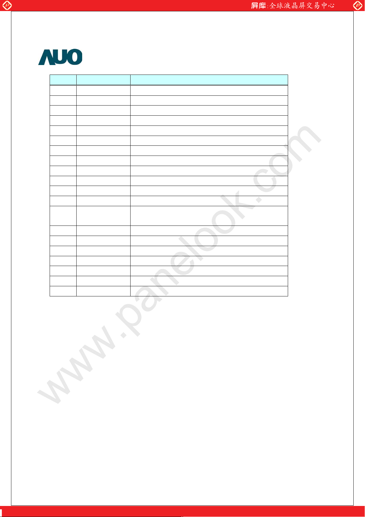
3.2 Interface Connections
z
LCD connector: FI-RE51S-HF (JAE)
Mating connector: FI-RE51S-HL (JAE)
z
PIN # Signal Name Description
1 VDD 12V power supply
2 VDD 12V power supply
3 VDD 12V power supply
4 VDD 12V power supply
5 VDD 12V power supply
6 NC No connection
7 GND Ground
8 GND Ground
9 GND Ground
10 RAX0- LVDS RAN
11 RAX0+ LVDS RAP
12 RAX1- LVDS RBN
13 RAX+ LVDS RBP
14 RAX2- LVDS RCN
15 RAX2+ LVDS RCP
16 GND Ground
17 RAXCLK- LVDS RCLKN
18 RAXCLK+ LVDS RCLKP
19 GND Ground
20 RAX3- LVDS RDN
21 RAX3+ LVDS RDP
22 RAX4- LVDS REN
23 RAX4+ LVDS REP
24 GND Ground
25 RBX0- LVDS RAN
26 RBX0+ LVDS RAP
27 RBX1- LVDS RBN
28 RBX1+ LVDS RBP
29 RE_2- LVDS RCN
30 RE_2+ LVDS RCP
31 GND Ground
www.panelook.com
©Copyright AU Optronics Corp.
2007 All Rights Reserved. T400HW02 V0
No Reproduction and Redistribution Allowed
One step solution for LCD / PDP / OLED panel application: Datasheet, inventory and accessory!
ʳ
9/32
www.panelook.com
Global LCD Panel Exchange Center
PIN # Signal Name Description
32 RBXCLK- LVDS RCLKN
33 RBXCLK+ LVDS RCLKP
34 GND Ground
35 RBX3- LVDS RDN
36 RBX3+ LVDS RDP
37 RBX4- LVDS REN
38 RBX4+ LVDS REP
39 GND Ground
40 LVDS_SCL I2C clock
41 LVDS_SDA I2C data
42 NC No connection
43 B-INT I2C BUS Enable (H/Open: enable, L: disable)
44
45 SET_ON2 Power on sequence( NC for stand alone mode)
46 SA_MODE Stand alone mode(L/Open: Standalone, H:SONY use only)
47 AGING_MODE Aging mode enable signal (H: Aging, L ; Normal)
48 BUS_SW I2C BUS Enable (H/Open: enable, L ; disable)
49 FRC_RST FRC-S reset
50 TCON_RDY FRC-S ready signal
51 Panel_ON Power on sequence(NC for stand alone mode)
Note: (1) All GND (ground) pins should be connected together and should also be connected to the LCD’s
metal frame. (2) All V
should be open without voltage input. (4)Pin assignment is refer to SONY BT2 board definition.
PANEL SEL Panel select signal output (Pull down)
(power input) pins should be connected together. (3) All NC (no connection) pins
DD
www.panelook.com
(NC for stand alone mode)
©Copyright AU Optronics Corp.
2007 All Rights Reserved. T400HW02 V0
No Reproduction and Redistribution Allowed
One step solution for LCD / PDP / OLED panel application: Datasheet, inventory and accessory!
ʳ
10/32
www.panelook.com
 Loading...