

AUO T370HW03 VQ Specification
Global LCD Panel Exchange Center
Model Name: T370HW03 VQ
( )Preliminary Specifications
(ϠϠϠϠ)Final Specifications
www.panelook.com
T370HW03 VQ Product Specification
Rev.0 0
Issue Date : 2011/1/25
© Copyright AUO Optronics Corp. 2009 All Rights Reserved. Page1 / 32
One step solution for LCD / PDP / OLED panel application: Datasheet, inventory and accessory!
www.panelook.com

Global LCD Panel Exchange Center
No
CONTENTS
RECORD OF REVISIONS
1 GENERAL DESCRIPTION
2 ABSOLUTE MAXIMUM RATINGS
3 ELECTRICAL SPECIFICATION
3-1 ELECTRIACL CHARACTERISTICS
3-2 INTERFACE CONNECTIONS
3-3 SIGNAL TIMING SPECIFICATION
www.panelook.com
T370HW03 VQ Product Specification
Rev.0 0
Contents
3-4 SIGNAL TIMING WAVEFORM
3-5 COLOR INPUT DATA REFERENCE
3-6 POWER SEQUENCE
3-7 BACKLIGHT SPECIFICATION
4 OPTICAL SPECIFICATION
5 MECHANICAL CHARACTERISTICS
6 RELIABILITY TEST ITEMS
7 INTERNATIONAL STANDARD
7-1 SAFETY
7-2 EMC
8 PACKING
8-1 DEFINITION OF LABEL
8-2 PACKING METHODS
8-3 PALLET AND SHIPMENT INFORMATION
9 PRECAUTION
9-1 MOUNTING PRECAUTIONS
9-2 OPERATING PRECAUTIONS
9-3 ELECTROSTATIC DISCHARGE CONTROL
9-4 PRECAUTIONS FOR STRONG LIGHT EXPOSURE
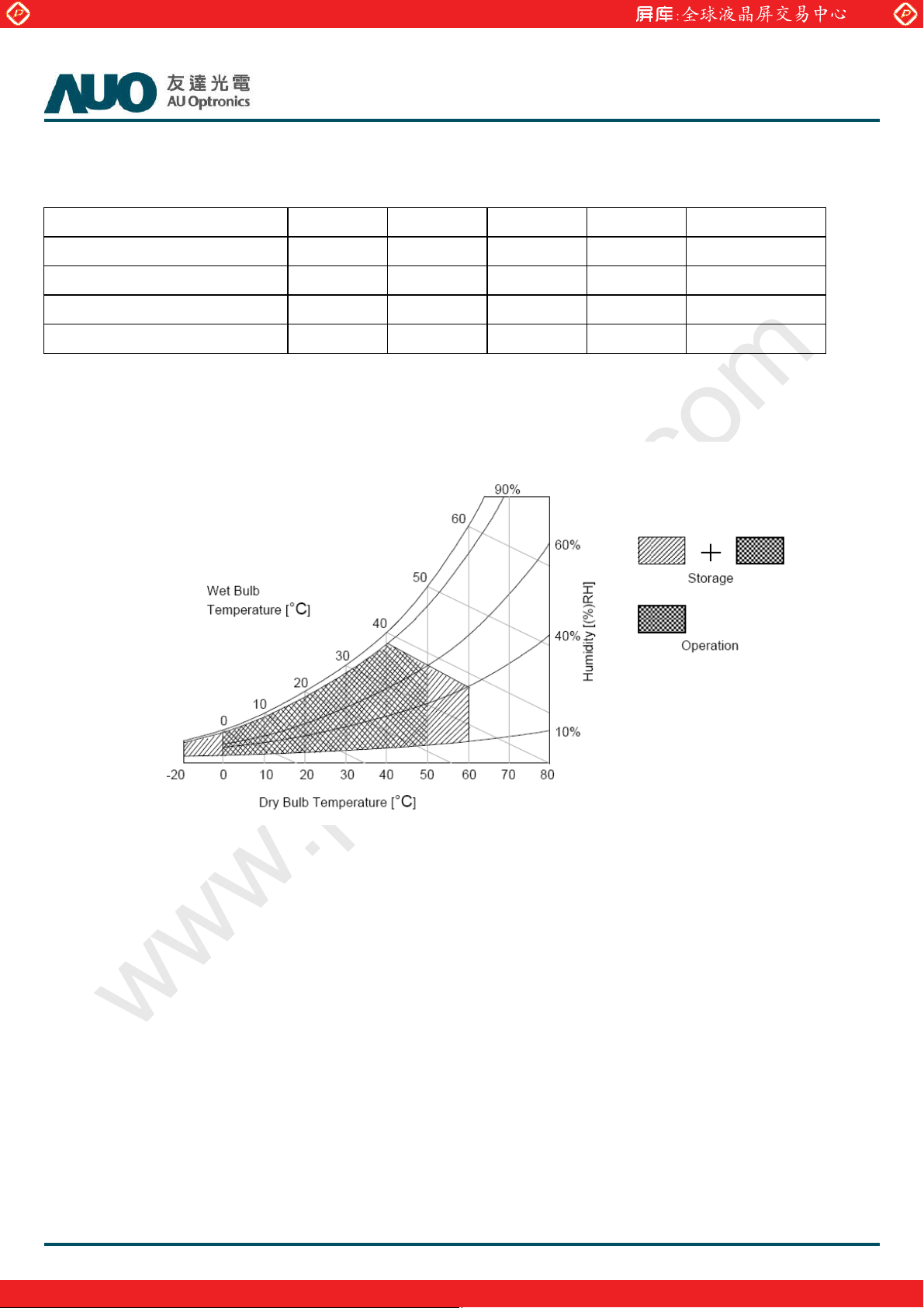
9-5 STORAGE
9-6 HANDLING PRECAUTIONS FOR PROTECT FILM
© Copyright AUO Optronics Corp. 2009 All Rights Reserved. Page2 / 32
One step solution for LCD / PDP / OLED panel application: Datasheet, inventory and accessory!
www.panelook.com
Global LCD Panel Exchange Center
Record of Revision
Version Date Page Description
0.0 2010/12/28 First release
www.panelook.com
T370HW03 VQ Product Specification
Rev.0 0
© Copyright AUO Optronics Corp. 2009 All Rights Reserved. Page3 / 32
One step solution for LCD / PDP / OLED panel application: Datasheet, inventory and accessory!
www.panelook.com
Global LCD Panel Exchange Center
www.panelook.com
T370HW03 VQ Product Specification
Rev.0 0
1. General Description
This specification applies to the 37.0 inch Color TFT-LCD Module T370HW03 VQ. This LCD module has a TFT active
matrix type liquid crystal panel 1,920x1,080 pixels, and diagonal size of 37.0 inch. This module supports 1,920x1,080
mode. Each pixel is divided into Red, Green and Blue sub-pixels or dots which are arranged in vertical stripes. Gray scale
or the brightness of the sub-pixel color is determined with a 8-bit gray scale signal for each dot.
The T370HW03 VQ has been designed to apply the 8-bit 2 channel LVDS interface method. It is intended to support
displays where high brightness, wide viewing angle, high color saturation, and high color depth are very important.
* General Information
Items Specification Unit Note
Active Screen Size 37.00 inch
Display Area 885.6(H) x 498.15(V) mm
Outline Dimension 877(H) x 516.8 (V) x 46.5(D) mm D: front bezel to T-con cover
Driver Element a-Si TFT active matrix
Bezel Opening 939 (H) x 531 (V) mm
Display Colors 8 bit, 16.7M Colors
Number of Pixels 1,920x1,080 Pixel
Pixel Pitch 0.4268 (H) x 0.4268(W) mm
Pixel Arrangement RGB vertical stripe
Display Operation Mode Normally Black
Surface Treatment Anti-Glare, 3H Haze=2%
© Copyright AUO Optronics Corp. 2009 All Rights Reserved. Page4 / 32
One step solution for LCD / PDP / OLED panel application: Datasheet, inventory and accessory!
www.panelook.com
Global LCD Panel Exchange Center
www.panelook.com
T370HW03 VQ Product Specification
2. Absolute Maximum Ratings
The followings are maximum values which, if exceeded, may cause faulty operation or damage to the unit
Item Symbol Min Max Unit Conditions
Logic/LCD Drive Voltage VDD -0.3 14 VDC Note 1
Input Voltage of Signal Vin -0.3 4 VDC Note 1
BLU Input Voltage VDDB -0.3 28 VDC Note 1
BLU Brightness Control Voltage Vdim -0.3 7 VDC Note 1
Note 1: Duration: 50 msec.
Rev.0 0
© Copyright AUO Optronics Corp. 2009 All Rights Reserved. Page5 / 32
One step solution for LCD / PDP / OLED panel application: Datasheet, inventory and accessory!
www.panelook.com
Global LCD Panel Exchange Center
www.panelook.com
T370HW03 VQ Product Specification
Rev.0 0
3. Electrical Specification
The T370HW03 VQ requires two power inputs. One is employed to power the LCD electronics and to drive the TFT array
and liquid crystal. The second input for BLU is to power inverter.
3.1 Electrical Characteristics
3.1.1: DC Characteristics
Parameter Symbol
Unit Note
Min. Typ. Max
LCD
Power Supply Input Voltage VDD 10.8 12 13.2 VDC
Power Supply Input Current IDD -- 0.93 1.023 A 1
Power Consumption PC -- 11.16 12.276 Watt 1
Value
Inrush Current I
Input Differential Voltage
LVDS
Interface
Differential Input High Threshold Voltage VTH +100 -- +300 mVDC 3
Differential Input Low Threshold Voltage VTL -300 -- -100 mVDC 3
Input Common Mode Voltage V
-- -- 3 A 2
RUSH
Ю
ЮV
ID
1.1 1.25 1.4 VDC 3
ICM
200 400 600 mV
3
DC
Input High Threshold Voltage VTH 2.7 -- 3.3 VDC 4 CMOS
Interface
Backlight Power Consumption P
Input Low Threshold Voltage V
0 -- 0.6 VDC 4
TL
BL
81 90 99
Watt
Life Time 50000 Hours
© Copyright AUO Optronics Corp. 2009 All Rights Reserved. Page6 / 32
One step solution for LCD / PDP / OLED panel application: Datasheet, inventory and accessory!
www.panelook.com

Global LCD Panel Exchange Center
s
3.1.2: AC Characteristics
www.panelook.com
T370HW03 VQ Product Specification
Rev.0 0
Parameter Symbol
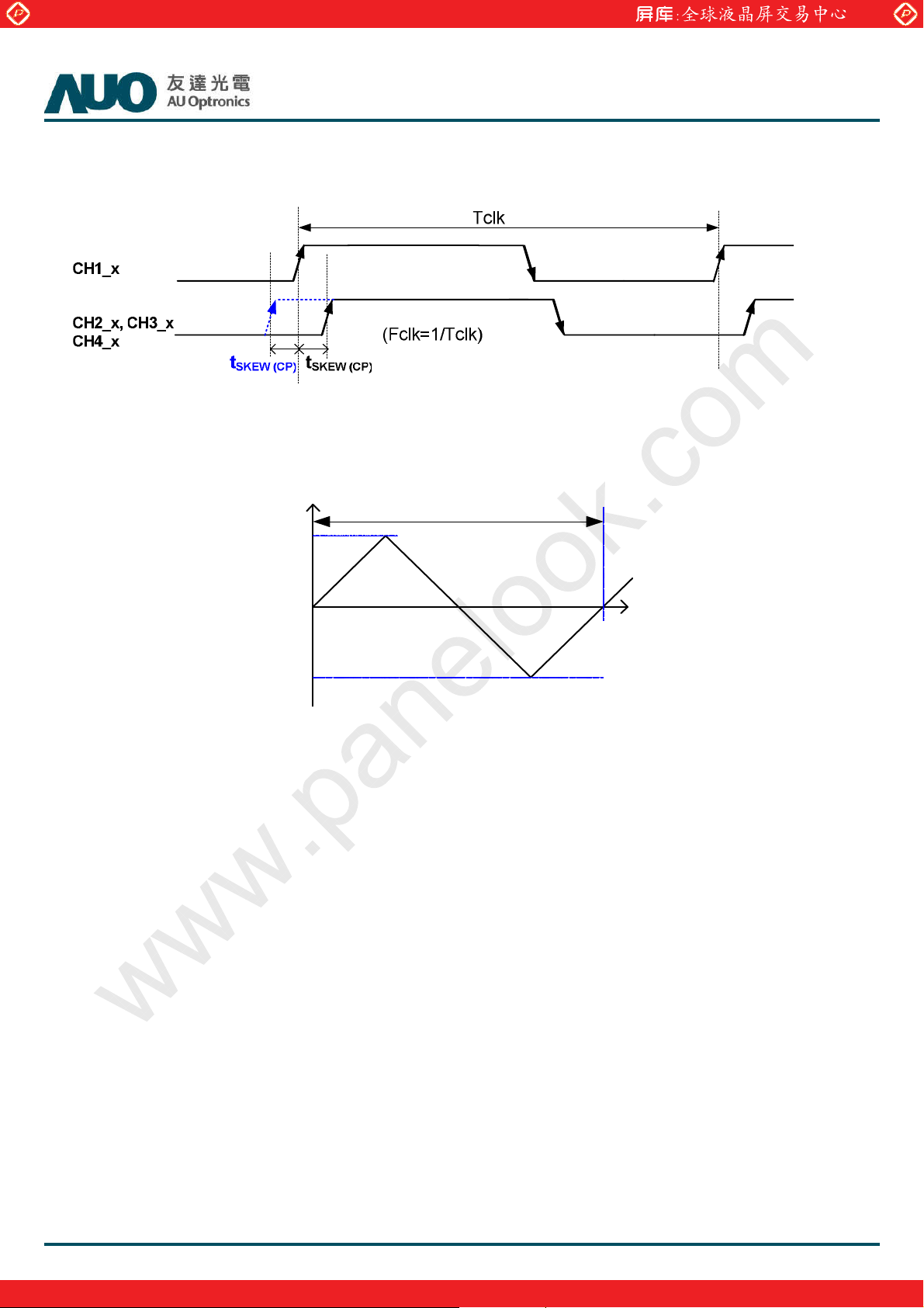
Input Channel Pair Skew Margin
Receiver Clock : Spread Spectrum
LVDS
Interface
Modulation range ʳ
Receiver Clock : Spread Spectrum
Modulation frequencyʳ
Receiver Data Input Margin
Fclk = 85 MHz
Fclk = 65 MHzʳ
Note :
1. Test Condition:
(1) V
= 12.0V
DD
(2) Fv = Type Timing, 60Hz, 120Hz or Other
(3) Fclk= Max freq.
(4) Temperature = 25 к
(5) Typ. Input current : White Pattern
Max. Input current: Heavy loading pattern defined by AUO
>> refer to “Section:3.3 Signal Timing Specification, Typical timing”
2. Measurement condition : Rising time = 400us
Value
Unit Note
Min. Typ. Max
t
SKEW (CP)
Fclk_ssʳ
-500 -- +500 ps 5
Fclk
-3%ʳ
--ʳ
Fclk
+3%ʳ
MHzʳ 6
Fssʳ 30ʳ --ʳ 200ʳ KHzʳ 6
ʳ
tRMGʳ -0.4
-0.5ʳ
--ʳ
--ʳ
0.4
0.5ʳ
nsʳ 7
3. V
= 1.25V
ICM
LVDS -
LVDS +
V
ICM
GND
0V
GND
10%
400
|VID|
V
90%
DD
μ
V
TH
|VID|
V
TL
|VID|
© Copyright AUO Optronics Corp. 2009 All Rights Reserved. Page7 / 32
One step solution for LCD / PDP / OLED panel application: Datasheet, inventory and accessory!
www.panelook.com
Global LCD Panel Exchange Center
www.panelook.com
T370HW03 VQ Product Specification
4. The measure points of V
5. Input Channel Pair Skew Margin
Note: x = 0, 1, 2, 3, 4
and V
IH
are in LCM side after connecting the System Board and LCM.
IL
6. LVDS Receiver Clock SSCG (Spread spectrum clock generator) is defined as below figures
Rev.0 0
Fclk_ss(max)
Fclk
Fclk_ss(min)
1/F
SS
© Copyright AUO Optronics Corp. 2009 All Rights Reserved. Page8 / 32
One step solution for LCD / PDP / OLED panel application: Datasheet, inventory and accessory!
www.panelook.com
Global LCD Panel Exchange Center
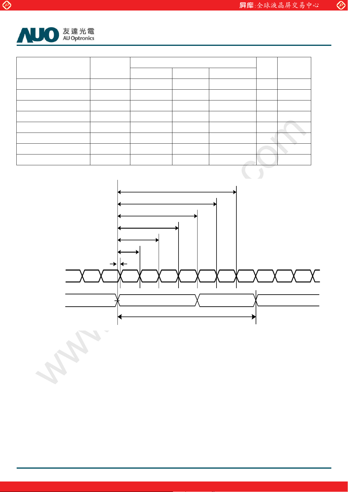
7. Receiver Data Input Margin
www.panelook.com
T370HW03 VQ Product Specification
Rev.0 0
Parameter Symbol
Min Type Max
Input Clock Frequency Fclk Fclk (min) -- Fclk (max) MHz T=1/Fclk
Input Data Position0 tRIP1 -|tRMG| 0 |tRMG| ns
Input Data Position1 tRIP0 T/7-|tRMG| T/7 T/7+|tRMG| ns
Input Data Position2 tRIP6 2T/7-|tRMG| 2T/7 2T/7+|tRMG| ns
Input Data Position3 tRIP5 3T/7-|tRMG| 3T/7 3T/7+|tRMG| ns
Input Data Position4 tRIP4 4T/7-|tRMG| 4T/7 4T/7+|tRMG| ns
Input Data Position5 tRIP3 5T/7-|tRMG| 5T/7 5T/7+|tRMG| ns
Input Data Position6 tRIP2 6T/7-|tRMG| 6T/7 6T/7+|tRMG| ns
Rating
Unit Note
tRIP2
tRIP3
tRIP4
tRIP5
LVDS-Rx
Input Data
LVDS-Rx
Input Clock
tRIP6
tRIP0
tRIP1
Rx1 Rx0 Rx6 Rx5 Rx4 Rx3 Rx2 Rx1 Rx 0 Rx 6Rx2Rx3
V
= 0V
dif f
1/Fclk=T
© Copyright AUO Optronics Corp. 2009 All Rights Reserved. Page9 / 32
One step solution for LCD / PDP / OLED panel application: Datasheet, inventory and accessory!
www.panelook.com
Global LCD Panel Exchange Center
3.2 Interface Connections
www.panelook.com
T370HW03 VQ Product Specification
Rev.0 0
LCD connector:
Mating connector: LVDS P-TWO 187059-5122
187059-51221 (P-TWO, LVDS connector)
1 Reserved AUO Internal Use Only (NC)
2 Reserved AUO Internal Use Only (NC)
3 Reserved AUO Internal Use Only (NC)
4 Reserved AUO Internal Use Only (NC)
Reserved
5
NC or GND: 8 bit
(BITSEL)
Reserved
High(3.3V) : Rotate enable(Data mirror)
6
(ROTATE)
Open/Low(GND) : Normal
7 LVDS_SEL Open/High(3.3V) for NS, Low(GND) for JEIDA
Reserved
Duty: TBD%~100% (0~3.3V)
8
(DIM_IN)
Reserved
Frequency: 140~160Hz
Duty: TBD%~100% (0~3.3V)
9
(DIM_OUT)
Frequency: 150Hz
Reserved
Low(GND)/Open : DCR Function Disable(Bypass DIM_IN)
10
(DCR_Enable)
High(3.3V) : DCR Function Enable
11 GND Ground
12 CH1_0- LVDS Channel 1, Signal 0-
13 CH1_0+ LVDS Channel 1, Signal 0+
14 CH1_1- LVDS Channel 1, Signal 1-
15 CH1_1+ LVDS Channel 1, Signal 1+
16 CH1_2- LVDS Channel 1, Signal 2-
17 CH1_2+ LVDS Channel 1, Signal 2+
18 GND Ground
19 CH1_CLK- LVDS Channel 1, Clock -
20 CH1_CLK+ LVDS Channel 1, Clock +
21 GND Ground
22 CH1_3- LVDS Channel 1, Signal 3-
23 CH1_3+ LVDS Channel 1, Signal 3+
24 Reserved AUO Internal Use Only (NC)
25 Reserved AUO Internal Use Only (NC)
26 NC NC
© Copyright AUO Optronics Corp. 2009 All Rights Reserved. Page10 / 32
One step solution for LCD / PDP / OLED panel application: Datasheet, inventory and accessory!
www.panelook.com
 Loading...